

Results 7,121 to 7,130 of 12091
Thread: Anandtech News
-
06-29-17, 07:09 AM #7121
Anandtech: Joint Venture Dispute Between Toshiba and Western Digital Escalates, Toshi
Due to serious financial difficulties, Toshiba is trying to sell off their stake of their very successful flash memory business to keep the rest of the company afloat. Western Digital, as a result of their acquisition of SanDisk last year, owns half of the joint venture that Toshiba is selling their stake in. Western Digital would prefer to buy out Toshiba's share to strengthen their own position in the market, but they have struggled to keep up with the bidding as offers climb past ¥2T ($17.8B). The leading bidder has been a consortium with backing from the Japanese government and many major Japanese corporations through the Innovation Network Corporation of Japan and the Development Bank of Japan, as well as investments from Bain Capital Private Equity and rival memory manufacturer SK Hynix.
Western Digital has asserted that the terms of their joint ventures with Toshiba require SanDisk's approval before Toshiba can sell their stake, and Western Digital has not given their consent to any sale. This has not stopped Toshiba from continuing to negotiate a sale, so Western Digital has predictably taken legal action. In May Western Digital began arbitration proceedings through the ICC International Court of Arbitration. Toshiba made a partial concession by rolling back the spin-off of some of the memory business assets they were preparing to sell, but their overall plan did not change and Western Digital was not placated. Earlier this month, Western Digital filed for an injunction preventing Toshiba's sale until the arbitration was resolved. Western Digital's action was filed in the Superior Court of California for the County of San Francisco.
As the dispute developed, Western Digital and Toshiba continued normal day to day operations of their business, including announcements around Computex about their upcoming SSDs using their 64-layer BiCS3 3D NAND, and the announcement earlier this week of their development of 96-layer BiCS4 3D NAND. Toshiba was hoping to complete a deal with the winning bidder at a shareholder meeting yesterday. In the weeks leading up to that meeting, Toshiba had to issue several reminders of how desperate their financial state is: disclosing new legal actions against them by investors seeking damages pertaining to Toshiba's accounting scandals, announcing that the Tokyo and Nagoya stock exchanges are moving toward delisting Toshiba, and revising their outlook for fiscal year 2016 to reflect a negative shareholder equity of (¥581.6B). Meanwhile, Western Digital reiterated their objection to Toshiba selling the memory business to a third party and warned several third parties that they would view participation in the sale as tortious interference. Most recently, Western Digital also reportedly resubmitted its bid for Toshiba's memory business with an offer around ¥2 trillion, close to the amount offered by the consortium Toshiba had previously selected as the preferred bidder. Toshiba for their part has made no mention of Western Digital's offer.
In the aftermath of yesterday's shareholder meeting, Toshiba made several announcements. As expected, Toshiba was not able to finalize a sale of the Toshiba Memory Corporation subsidiary they have consolidated the memory-related assets under, but they are continuing to negotiate with the consortium. Toshiba announced plans for further investment in the joint venture's Fab 6 in Yokkaichi, Japan, and questioned whether SanDisk would jointly invest in the 3D NAND fab. Toshiba also announced that it has filed a lawsuit in the Tokyo District Court against Western Digital alleging unfair competition and seeking an injunction and damages. Toshiba claims that Western Digital is exaggerating their consent rights and also alleges that Western Digital has improperly obtained Toshiba trade secrets by transferring some employees from SanDisk to Western Digital whom have access to Toshiba confidential information through the joint ventures.
Western Digital has responded by denying Toshiba's allegations of improper handling of trade secrets, and claims that Toshiba has taken retaliatory action by cutting off some of Western Digital's employees' access to shared databases and facilities. Western Digital reaffirmed their intent to continue fully participating and investing in the joint ventures, and claimed to have not yet received the legal filings pertaining to Toshiba's lawsuit in Tokyo. Western Digital again claimed that the terms of their joint ventures requires that disputes be resolved through the arbitration process, making it clear they consider Toshiba's lawsuit improper.
The SanDisk request for an injunction in the California court is scheduled for a hearing on July 14. It appears that there will not be any quick resolution to this dispute unless Toshiba's money troubles force them to accept Western Digital's bid. The consortium that Toshiba is trying to sell to has not made any collective public statements, but we expect continued leaks about the state of their offer.
More...
-
06-29-17, 08:13 AM #7122
Anandtech: AMD Launches Ryzen PRO CPUs: Enhanced Security, Longer Warranty, Better Qu
This morning AMD is introducing their Ryzen PRO processors for business and commercial desktop PCs. The new lineup of CPUs includes the Ryzen 3 PRO, Ryzen 5 PRO and Ryzen 7 PRO families with four, six, or eight cores running at various frequencies. A superset to the standard Ryzen chips, the PRO chips have the same feature set as other Ryzen devices, but also offer enhanced security, 24 months availability, a longer warranty and promise to feature better chip quality.
AMD Ryzen Pro: The Family Portrait
The AMD Ryzen PRO lineup of processors consists of six SKUs that belong to the Ryzen 7, Ryzen 5 and Ryzen 3 families targeting different market segments and offering different levels of performance. As one would expect, the Ryzen 7 PRO models are aimed at workstation applications and thus have all eight cores with simultaneous multithreading enabled, the Ryzen 5 PROmodels are designed for advanced mainstream desktops and therefore have four or six cores with SMT, whereas the Ryzen 3 PRO models are aimed at office workloads that work well on quad-core CPUs without SMT. The specifications of the Ryzen 7 PRO and the Ryzen 5 PRO resemble those of regular Ryzen processors. Meanwhile, the Ryzen 3 PRO are the first chips from the Ryzen 3 lineup and thus give us a general idea what to expect from such products: four cores without SMT operating at 3.1 – 3.5 GHz base frequency along with 2+8 MB of cache.
Just like other Ryzen CPUs, all the Ryzen PRO chips fully support ECC technology, but with certain limitations when it comes to data transfer rates and memory modules — these are peculiarities of the controller and the PRO moniker cannot change them. One of the things to note is that AMD used only DDR4-2400 memory for its internal testing of the Ryzen PRO CPUs, thus, expect PC makers to use the same speed DRAM for their desktops as well.AMD Ryzen PRO Specifications Cores/Threads Frequency Cache TDP Base Boost L2 L3 Ryzen 7 PRO 1700X 8/16 3.5 GHz 3.7 GHz 4 MB 16 MB 95 W Ryzen 7 PRO 1700 3 GHz 3.7 GHz 65 W Ryzen 5 PRO 1600 6/12 3.2 GHz 3.6 GHz 3 MB Ryzen 5 PRO 1500 4/8 3.5 GHz 3.7 GHz 2 MB Ryzen 3 PRO 1300 4/4 3.5 GHz 3.7 GHz 8 MB Ryzen 3 PRO 1200 4/4 3.1 GHz 3.4 GHz
In fact, when it comes to general feature set, all AMD Ryzen PRO CPUs support the same capabilities as their non-PRO brethren do, including AMD’s SenseMi, Precision Boost, Extended Frequency Range, Neural Net Prediction and so on. In fact, there is the AMD Ryzen 7 PRO 1700X CPU in the lineup with extended performance and 95 W TDP (the first for any AMD PRO platform). Meanwhile, there are four things that the Ryzen PRO bring to the table: enhanced security features, enterprise-class manageability, processor and platform longevity and enhanced quality (which we are going to touch upon later).
With the launch of the Ryzen PRO, AMD offers its iGPU-less processors for business desktops for the first time ever. Previously the company only offered its A PRO-series APUs with integrated graphics and TDP ranging from 35 to 65 W. By contrast, the new CPU are offered with 65 – 95 thermal envelops, which means that we are not going to see ultra-small form-factor workstations running AMD Ryzen PRO, but may finally see full-sized desktops.
It makes sense to note that all Ryzen PRO CPUs, including the highest performing and the most affordable SKUs, will support all of the advertised enterprise/business-grade capabilities. AMD is especially proud about that because its rival Intel does not support enterprise features (such as vPro) on lower-end Core i3 models. At this point AMD does not disclose prices of its Ryzen PRO CPUs and the only metrics that AMD uses for comparison against competing SKUs is performance, not MSRPs or TDPs.
Such comparison shows that AMD’s Ryzen PRO lineup for desktops can cover a wider range of performance requirements than Intel’s mainstream vPro offerings do. For example, the AMD Ryzen PRO 1700X does not have a direct competitor from Intel, according to AMD. Which may indicate that vPro supporting Xeon E5s are considerably more expensive than the Ryzen PRO 1700X is going to be. In addition, AMD’s Ryzen 3 PRO 1200 also does not have a corresponding rival from the Core i3 lineup from performance point of view, based on AMD’s comparison. However, since Intel also offers Core i7 and Core i5 CPUs with TDP reduced to 35 W (for which AMD does not have announced competitors in the Ryzen PRO range), such performance-focused comparison does not display a complete picture.AMD Ryzen PRO Competitive Positioning Based on Performance AMD Intel Model Key Features Price Model Key Features Price Ryzen 7 PRO 1700X 8C/16T, 3.5/3.7 GHz, 20 MB cache, 95 W ? - - - Ryzen 7 PRO 1700 8C/16T, 3/3.7 GHz, 20 MB cache, 65 W Core i7-7700 4C/8T, 3.6/4.2 GHz, 8 MB cache, 65 W $303 - $312 Ryzen 5 PRO 1600 6C/12T, 3.2/3.6 GHz, 19 MB cache, 65 W Core i5-7500 4C/4T, 3.4/3.8 GHz, 6 MB cache, 65 W $192 - $202 Ryzen 5 PRO 1500 4C/8T, 3.5/3.7 GHz, 18 MB cache, 65 W Ryzen 3 PRO 1300 4C/8T, 3.5/3.7 GHz, 10 MB cache, 65 W Core i3-7100 2C/4T, 3.9 GHz, 3 MB cache, 51 W $117 Ryzen 3 PRO 1200 4C/8T, 3.1/3.4 GHz, 10 MB cache, 65 W - - -
New AMD Secure Technologies
Now, time to talk about security features of the AMD Ryzen PRO platform. For years AMD’s processors for business PCs supported security technologies (collectively known as AMD Secure Processor and Platform Security Processor before that) enabled by the ARM TrustZone platform with the ARM Cortex-A5 core. AMD’s previous-gen PRO-series APUs included Secure Boot, Content Protection, per-Application security, fTPM 2.0, and support for Microsoft Device Guard, Windows Hello, fingerprint security, data protection and so on. The Ryzen PRO adds Transparent Secure Memory Encryption (TSME) on top of them.
To explain what TSME is, it makes sense to refer to AMD’s Zen memory encryption technologies in general. The Zen microarchitecture features two important technologies: Secure Memory Encryption (SME) and Secure Encrypted Virtualization (SEV) that protect data in DRAM using a dedicated AES-128 engine.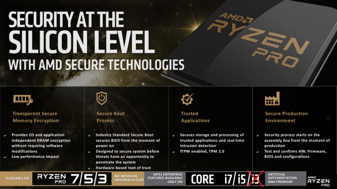
When data is stored on storage devices, it is usually encrypted, but when it is processed, it is almost never is, leaving possibilities to steal certain confidential things. As the name suggests, Secure Memory Encryption encrypts content of DRAM in a bid to eliminate data snooping by unauthorized programs or administrators (this is more likely to happen in a server/datacenter environment, but still). This feature will be particularly important for NVDIMMs going forward as they store data even after unplugged from their hosts.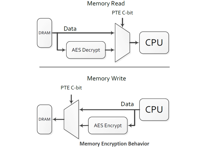
The SME encrypts data when it is written to DRAM and decrypts it when it is read. The AES-128 key is generated NIST SP 800-90 compliant hardware random number generator and then managed by the AMD-SP hardware (thus, in a secure environment only). Although a dedicated engine performs the encryption/decryption, the process still takes time and thus adds latency for memory accesses. AMD claims that the actual performance impact is not significant, but will have to test it before making any conclusions of our own. AMD’s Zen microarchitecture supports full and partial memory encryption for cases when performance is a concern. Meanwhile, both require OSes and software to be modified in order to work properly. Meanwhile, AMD’s processors also support Transparent SME mode that that encrypts DRAM completely, can be enabled from BIOS and thus be used with legacy OSes and programs. At this point Transparent SME is the only type of SME supported by the Ryzen Pro, but AMD’s EPYC processors support all of them.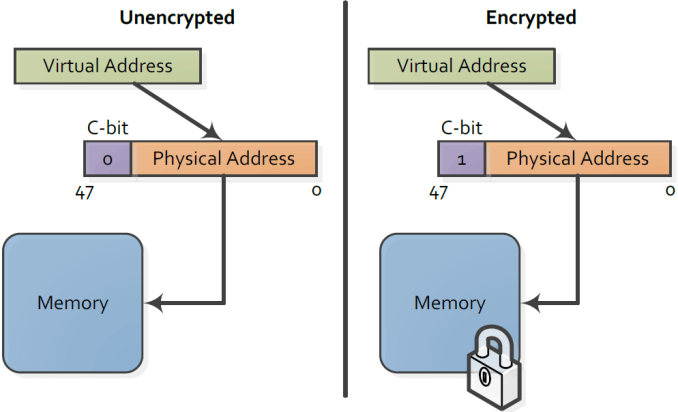
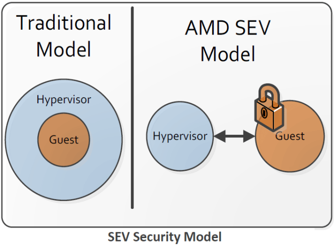
The Secure Encrypted Virtualization in many ways resembles the SME, but in this case, it enables owners to encrypt virtual machines, isolating them from each other, hypervisor and hosting software. The SEV is an extension to AMD’s virtualization architecture that uses the same hardware as the SME to protect/sandbox selected VMs using different AES-128 keys and eliminating some of the security threats particularly in datacenter environments. As the SEV uses different keys for different VMs, it does not work with TSME. By contrast, SEV is fully enabled on AMD’s EPYC processors (it will be interesting to see whether Threadripper chips support the feature as well).
One thing that should be noted is that both SME and SEV should be supported not only by processors themselves, but also on the platform and the software levels. With the exception of TSME mode (which will still require BIOS/chipset support), it will take some time before actual systems can take advantage of the new technologies supported by AMD’s Zen microarchitecture. A good thing is that owners of the Ryzen PRO will be able to use TSME already this year and this is where AMD’s new business platform excels Intel’s Core-series offerings.
Enterprise Manageability and Reliability
In addition to security capabilities, business PCs require some other hardware features as well.

First off, the Ryzen PRO platforms support DASH management protocol and therefore PCs featuring the chips can be remotely managed using tools based on this industry standard developed by vendors of appropriate computers. AMD Pro-series processors have supported DASH for years, no changes here.
Secondly, AMD’s Ryzen PRO platforms support 18-month platform stability and 24-month processor availability. AMD guarantees that the Ryzen PRO chips it launches this year will be available for two more years without changes to software, enabling business customers to buy and deploy new systems running the CPUs without modifying the software they use.
Finally, all AMD Ryzen PRO CPUs are covered with a 36-month limited warranty, up from 12-month warranty for consumer processors. The reason why AMD offers extended warranty for its business CPUs (apart from the fact that its customers demand this) is because it uses wafers with highest yields/least amount of defective parts to build the Ryzen Pro. AMD believes that wafers with the lowest manufacturing variability provide chips that are “set to meet long term reliability”.

Available This Fall
AMD promises to share more information about its Ryzen PRO CPUs and supporting platforms on August 29, 2017. The company does not say that actual systems will be available on this date, but since the chip designer already disclosed plans to ship Ryzen PRO in the second half of this year, it is safe to say that at least some Ryzen Pro-based desktops will ship this fall.
As for vendors, expect the usual workstation/commercial PC makers like Dell, HP, Lenovo and other to offer desktops powered by AMD’s Ryzen Pro.
Gallery: AMD Ryzen PRO Presentation


More...
-
06-29-17, 09:36 AM #7123
Anandtech: AMD Inadvertently Reveals Ryzen 3 1300 & 1200 Details
If you were paying close attention to this morning’s announcement of AMD’s new Ryzen Pro SKUs, then you likely noticed something interesting: the non-X PRO chips all have the same performance specifications as their standard consumer counterparts. Specifically, both of the non-X PRO SKUs with existing Ryzen 5 & 7 counterparts have the same core counts, clockspeeds, and TDPs. And for the final 2 Ryzen PRO 3 SKUS? Well, AMD has inadvertently shown their hand here when it comes to forthcoming Ryzen 3.
With the release of the Ryzen PRO 3 specifications, AMD has now confirmed what we’ve been suspecting for the Ryzen 3 specifications for a while now. Ryzen 3 is a quad-core CPU without SMT, so we’re looking at just 4 threads instead of 8, albeit 4 threads without any of the resource contention SMT can sometimes cause. On which matter, it’s worth pointing out that AMD has already previously commented that Ryzen 3 will use the same die as Ryzen 5 and Ryzen 7, so we’re looking at 4 cores distributed over 2 CCXs, like the Ryzen 5 1400 & 1500X.
Similarly, AMD’s reveal indicates that Ryzen 3 will have the same cache structure as the lowest-end Ryzen 5, the 1400. That means just half of the chip’s total 16MB of L3 cache is enabled. However each core still retains its full 512KB of L2 cache. Finally, this inadvertent reveal also confirms that TDPs for the lowest-end members of the Ryzen family will stick with the same 65W TDP as all but the highest-performance Ryzen chips.AMD Ryzen 5 & 3 SKUs Cores/
ThreadsBase/
TurboXFR L3 TDP Cost Cooler Ryzen 5 1600X 6/12 3.6/4.0 +100 16 MB 95 W $249 - Ryzen 5 1600 6/12 3.2/3.6 +100 16 MB 65 W $219 Spire Ryzen 5 1500X 4/8 3.5/3.7 +200 16 MB 65 W $189 Spire Ryzen 5 1400 4/8 3.2/3.4 +50 8 MB 65 W $169 Stealth Ryzen 3 1300* 4/4 3.5/3.7 TBD 8 MB 65 W TBD - Ryzen 3 1200* 4/4 3.1/3.4 TBD 8 MB 65 W TBD -
Of course, it should be noted here that AMD’s accidental reveal doesn’t mean that the 1300 & 1200 will be the only Ryzen 3 chips we’ll see. Just like the Ryzen 5 and 7 only had a couple of PRO counterparts, it’s likely that the story will be the same for the Ryzen 3 series. In particular, Ian suspects a Ryzen 3 1300X will show up, but we shall see in due time…
More...
-
06-29-17, 10:19 AM #7124
Anandtech: Western Digital Launches New My Passport Ultra HDDs: New Enclosure, Up to
Western Digital this week refreshed its My Passport Ultra lineup of small form-factor external HDDs. The new hard drives use a new enclosure and come with software that backs up data not only from local PCs, but also from social networks and cloud services. As for capacity and interfaces, the new HDDs continue to offer up to 4 TB of storage space and utilize a USB 3.0 interface.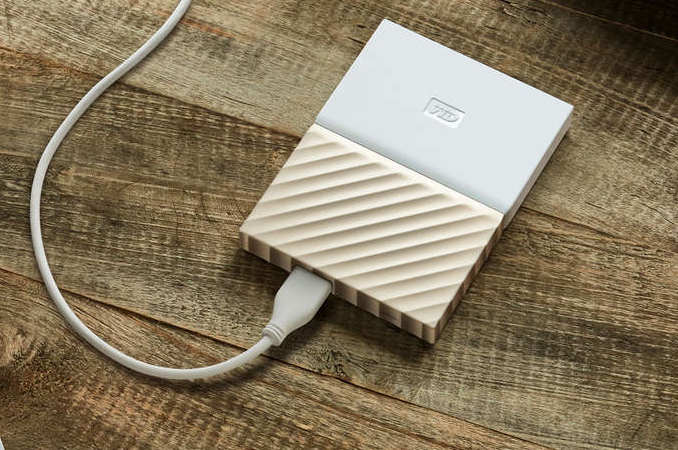
The new WD My Passport Ultra external HDDs come in a new metallic enclosure with metallic and matte black gray or white gold finishes that mimics design of other external storage devices by the company. The 1 TB drive uses a thinner enclosure that measures 13.5 mm (0.53”), whereas the models with 2 TB, 3 TB and 4 TB capacities are 21.5 mm (0.85”) thick.
Apart from the new enclosure, the new HDDs feature automatic WD Backup software for local data and content, as well as the company’s new WD Discovery software that backs up users’ data from Facebook, Instagram, Dropbox and Google Drive. By using both software suites, users can consolidate their data from different sources on a single device. Meanwhile, to protect the data, Western Digital offers its WD Backup software that relies on AES-256 hardware encryption.
Western Digital is not disclosing whether they're using PMR or SMR technology on the hard drives contained within. Nor are we able to accurately guess the number of platters in the drives, as the thickness of the external enclosures means it's impossible to determine whether the company is using 2.5”/12.5 mm or 2.5”/15 mm HDDs.
Just like their predecessors, the new Western Digital My Passport Ultra drives are covered by a three-year limited warranty. The new drives are available from wd.com as well as from select retailers around the world. The most affordable 1 TB version costs $79.99, whereas the highest-capacity SKU is available for $139.99, which is $20 lower than the My Passport Ultra HDD 4 TB released a year ago.List of WD’s 2017 My Passport Ultra Drives Capacity Model Dimensions
H×W×TInterface Compatibility Color 4 TB WDBFKT0040BGD-WESN 110×81.5×21.5 mm
4.33×3.21×0.85 inchUSB
3.0/2.0Windows 7, 8.1, 10.
Requires formatting
for other OSes.White-Gold WDBFKT0040BGY-WESN Black-Gray 3 TB WDBFKT0030BGY-WESN Black-Gray WDBFKT0030BGD-WESN White-Gold 2 TB WDBFKT0020BGY-WESN Black-Gray WDBFKT0020BGD-WESN White-Gold 1 TB WDBTLG0010BGY-WESN 110×81.5×13.5 mm
4.33×3.21×0.53 inchBlack-Gray WDBTLG0010BGD-WESN White-Gold

Related Reading:
- Western Digital Expands My Passport External USB 3.0 Drives To 4 TB
- Western Digital Announces My Passport SSD: Up to 1 TB, AES-256, USB-C
More...
-
06-29-17, 01:52 PM #7125
Anandtech: G.Skill Announces Quad-Channel DDR4-4200 Kit for Intel Skylake-X CPUs
G.Skill this past week has formally announced its quad-channel memory kits designed for the latest Intel Core i7 (Skylake-X) CPUs and the Intel X299 platform. The flagship 64 GB Trident Z kit boasts a 4200 MT/s data transfer rate, a rather notable step up from the company's "entry-level" 3600 MT/s kit. In addition, G.Skill is also introducing its new Trident Z Black series dual-channel DDR4-4400 kit for Intel’s Kaby Lake-X processors.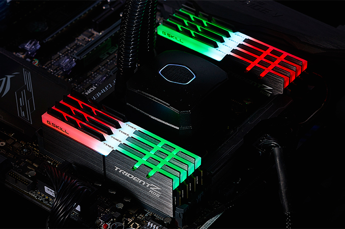
G.Skill’s lineup of memory kits for the Intel X299 platform consists of 8 GB and 16 GB Trident and Trident Z RGB DIMMs based on Samsung’s popular 20nm-fabbed 8 Gb DDR4 DRAM modules. The various kits are available at 3600 MT/s, 3733 MT/s, 3800 MT/s, 4000 MT/s, and 4200 MT/s data transfer rates, while their voltages run from 1.35 to 1.4 V. As you'd expect, the higher clocked kits also come with higher latency, with latencies starting at CL16 and reaching CL19 by DDR4-4200 speeds. Which goes to show that even though Intel's Skylake-X and Kaby Lake-X CPUs can handle very high DRAM frequencies, the tradeoff between clocks and timings has not gone anywhere.
Meanwhile it's interesting to note that despite G.Skill's recent obsession with RGB lighting – resulting in the company offering RGB-equipped DIMMs for most of the Trident Z range – the fastest DDR4-4200 and DDR4-4400 kits are not available with RGB lighting. Keeping in mind that this kind of extreme DDR4 overclocking requires increased voltage and very “clean” power, it may not be easy to apply RGB to such DIMMs without affecting their stability. Still, keeping in mind that G.Skill itself demonstrated DDR4-4200 Trident Z RGB DIMMs in quad-channel mode at Computex, it is a matter of time before appropriate modules will hit the market.
G.Skill traditionally announces its new memory modules a little bit ahead of their retail launch and does not set MSRPs ahead of actual availability, so pricing has not yet been disclosed on the company's newest kits.G.Skill's Trident Z Memory for Intel's X299 Platform Speed CL Timing Voltage Kit Configuration Kit Capacity Family DDR4-3600 CL16 16-16-36 1.35 V 4×8 GB
8×8 GB32 GB
64 GBTrident Z
Trident Z RGBCL17 19-19-39 4×16 GB
8×16 GB64 GB
128 GBDDR4-3733 CL17 17-17-37 4×8 GB
8×8 GB32 GB
64 GBCL18 19-19-39 4×16 GB
8×16 GB64 GB
128 GBDDR4-3800 CL18 18-18-38 4×8 GB
8×8 GB32 GB
64 GBCL19 19-19-39 4×16 GB
8×16 GB64 GB
128 GBDDR4-4000 CL18 19-19-39 4×8 GB
8×8 GB32 GB
64 GBDDR4-4200 CL19 19-19-39 1.4 V 8×8 GB 64 GB Trident Z DDR4-4400 CL19 19-19-39 1.4 V (?) 2×8 GB 16 GB Trident Z Black
Related Reading:
- DRAM and Motherboard Makers Demonstrate Quad-Channel DDR4-4000+ Operation
- G.Skill Announces 16 GB DDR4-4333 Memory Kit for Intel Kaby Lake CPUs
- G.Skill Announces Trident Z RGB DDR4 Kits with 16 GB Modules, Up to 128 GB
- AMD Announces Ryzen AGESA 1.0.0.6 Update: Enables Memory Clocks Up To DDR4-4000
- Corsair Vengeance RGB DDR4 Memory Modules with LEDs Now on Sale
More...
-
06-29-17, 08:23 PM #7126
Anandtech: NVIDIA Releases 384.76 WHQL Game Ready Driver
A few weeks have passed since driver version 382.53, and it’s time again for another driver update from NVIDIA. Now onto release 384 with driver version 384.76, NVIDIA brings us a good number of bug fixes, along with a Game Ready and Game Ready VR title.
Starting things off, the new Release 384 driver branch doesn't bring anything new to the table as far as major features go – at least, nothing that NVIDIA has documented. Instead their efforts have been focused almost entirely on bug fixes and performance improvements. To that end, NVIDIA has addressed issues where Firefall would not run at all. GeForce GTX 1080/1070/1060 stuttering during gameplay in Prey 2 was also addressed, as was texture corruption in No Man’s Sky when SLI was enabled. GTX 970 SLI can now be enabled while Norton 360 is running, as opposed to just when Norton 360 is disabled or in Safe mode. Glitches in Doom (2016) under the Vulkan API were also fixed.
NVIDIA also resolved CPU bottlenecks that occur when 3DVision is enabled, as well as issues with DirectX 12 titles failing to capture via GameStream. Issues with choppy video playback on the Windows Store video app while V-Sync was off were fixed. Last and probably least, a typo was corrected in NVIDIA Control Panel for the Command & Conquer Tiberium Alliances name on the Stereoscopic 3D Compatibility page.
The Game Ready headliner for this edition is the LawBreakers “Rise Up” Open Beta while Spider-Man: Homecoming VR Experience is the token Game Ready VR title. Slated to launch on August 8th, LawBreakers is developed by Cliff Bleszinski, whose pedigree includes games from the Unreal and Gears of War series, and is a class/character-based sci-fi ‘hero shooter,’ similar to games like Overwatch and Team Fortress 2. NVIDIA has polished their drivers in preparation for the “Rise Up” Open Beta, which goes from June 30th to July 3rd. As for the Spider-Man, Spider-Man: Homecoming VR Experience is a free tie-in to the upcoming Spider-Man: Homecoming film, and will be available for download on June 30th. While Homecoming VR is not exactly a full game, and described in the title itself as a “VR experience,” NVIDIA has prepped their drivers in advance regardless.
Wrapping things up, NVIDIA has added an SLI profile for FIFA 17, as well as adding a “debug” option in the NVIDIA Control Panel Help menu, which removes all overclocking performance and power settings.
The updated drivers are available through the GeForce Experience Drivers tab or online at the NVIDIA driver download page. More information on this update and further issues can be found in the 384.76 release notes.
More...
-
06-29-17, 11:26 PM #7127
Anandtech: TechInsights Confirms Apples A10X SoC Is TSMC 10nm FF; 96.4mm2 Die Size
One of the more intriguing mysteries in the Apple ecosystem has been the question over what process the company would use for the A10X SoC, which is being used in the newly launched 2017 iPad Pro family. Whereas the A10 used in the iPhone was much too early to use anything but 16nm/14nm, the iPad Pro and A10X is coming in the middle of the transition point for high-end SoCs. 16nm is still a high performance process, but if a company pushes the envelope, 10nm is available. So what would Apple do?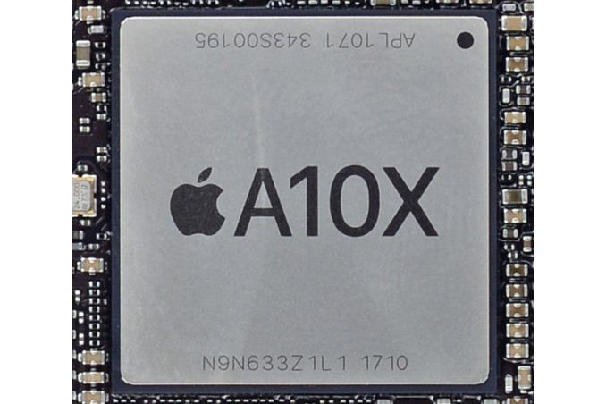
The answer, as it turns out, is that they’ve opted to push the envelope. The intrepid crew over at TechInsights has finally dissected an A10X and posted their findings, giving us our first in-depth look at the SoC. Most importantly then, TechInsights is confirming that the chip has been fabbed on TSMC’s new 10nm FinFET process. In fact, the A10X is the first TSMC 10nm chip to show up in a consumer device, a very interesting turn of events since that wasn’t what various production roadmaps called for (that honor would have gone to MediaTek’s Helio X30)
Apple is of course known for pushing the envelope on chip design and fabrication; they have the resources to take risks, and the profit margins to cover them should they not pan out. Still, that the A10X is the first 10nm SoC is an especially interesting development because it’s such a high-end part. Traditionally, smaller and cheaper parts are the first out the door as these are less impacted by the inevitable yield and capacity challenges of an early manufacturing node. Instead, Apple seems to have gone relatively big with what amounts to their 10nm pipecleaner part.
I say “relatively big” here because while the A10X is a powerful part, and big for a 10nm SoC, in terms of absolute die size it’s not all that big of a chip. In fact by Apple X-series SoC standards, it’s downright small: just 96.4mm2. This is 24% smaller than the 16nm A10 SoC (125mm2), and in fact is even 9% smaller than the A9 SoC (104.5mm2). So not only is it smaller than any of Apple’s 16nm SoCs, but it’s also about 20% smaller than the next-smaller X-series SoC, the A6X. Or, if you want to compare it to the previous A9X, Apple’s achieved a 34% reduction in die size. In other words, Apple has never made an iPad SoC this small before.
One key difference here however is that the X-series SoCs have never before been the leading part for a new process node. It has always been iPhone SoCs that have lead the charge – A9 at 16nm, A8 at 20nm, A7 at 28nm, etc. This does mean that as a pipecleaner part, Apple does need to be especially mindful of the risks. If an X-series SoC is to lead the charge for the 10nm generation, then it can’t be allowed to be too big. Not that this has stopped Apple from packing in three CPU cores and a 12-cluster GPU design.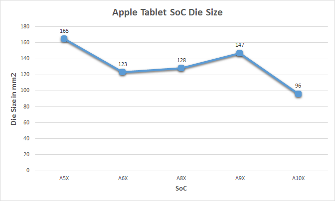
Speaking of size, TechInsights’ estimates for area scaling are quite interesting. Based on their accounting, they believe that Apple has achieved a 45% reduction in feature size versus 16nm, which is consistent with a full node’s improvement. This is consistent with TSMC’s earlier statements, but given the challenges involved in bringing newer processes to market, it’s none the less exciting to actually see it happening. For chip vendors designing products against 10nm and its 7nm sibling, this is good news, as small die sizes are the rule for pretty much everyone besides Apple.
A10X Architecture: A10 Enlarged
Diving a bit deeper, perhaps the biggest reason that A10X is as small as it is, is that Apple seems to have opted to be conservative with its design. Which again, for a pipecleaner part, is what you’d want to do.
We know from Apple’s official specifications that the A10X has 3 Fusion CPU core pairs, up from 2 pairs on A10, and 2 Twister CPU cores on A9X, all with 8MB of L2 cache tied to the CPU. Meanwhile the GPU in A10X is relatively unchanged; A9X shipped with a 12 cluster GPU design, and so does A10X. This means that Apple hasn’t invested their die space gains from 10nm in much of the way of additional hardware. To be sure, it’s not just a smaller A9X, but it’s also not the same kind of generational leap that we saw from A8X to A9X or similar iterations.Apple SoC Comparison A10X A9X A8X A6X CPU 3x Fusion
(Hurricane + Zephyr)2x Twister 3x Typhoon 2x Swift CPU Clockspeed ~2.36GHz 2.26GHz 1.5GHz 1.3GHz GPU 12 Cluster GPU PVR 12 Cluster Series7 Apple/PVR GXA6850 PVR SGX554 MP4 Typical RAM 4GB LPDDR4 4GB LPDDR4 2GB LPDDR3 1GB LPDDR2 Memory Bus Width 128-bit 128-bit 128-bit 128-bit Memory Bandwidth TBD 51.2GB/sec 25.6GB/sec 17.1GB/sec L2 Cache 8MB 3MB 2MB 1MB L3 Cache None None 4MB N/A Manufacturing Process TSMC 10nm FinFET TSMC 16nm FinFET TSMC 20nm Samsung 32nm
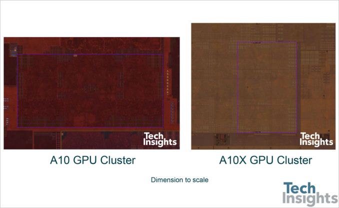
Unfortunately TechInsights’ public die shot release isn’t quite big enough or clean enough to draw a detailed floorplan from, but at a very high level we can make out the 12 GPU clusters on the left, along with the CPU cores to the right. Significantly, there aren’t any real surprises here. TechInsights heavily compares it to the A9X and there’s good reason to do so. IP blocks have been updated, but the only major change is the CPU cores, and those don’t take up a lot of die space relative to the GPU cores. This is what allows A10X to be more powerful than A9X while enjoying such a significant die size decrease.
As for the GPU in particular, Apple these days is no longer officially specifying whether they’re using Imagination’s PowerVR architecture in their chips. Furthermore we know that Apple is developing their own GPU, independent from Imagination’s designs, and that it will be rolled out sooner than later. With that said, even prior to today’s die shot release it’s been rather clear that A10X is not that GPU, and the die shot further proves that.
Apple’s developer documentation has lumped in the A10X’s GPU with the rest of the iOS GPU Family 3, which comprises all of the A9 and A10 family SoCs. So from a feature-set perspective, A10X’s GPU isn’t bringing anything new to the table. As for the die shot, as TechInsights correctly notes, the GPU clusters in the A10X look almost exactly like the A9X’s clusters (and the A10’s, for that matter), further indicating it’s the same base design.
Ultimately what this means is that in terms of design and features, A10X is relatively straightforward. It’s a proper pipecleaner product for a new process, and one that is geared to take full advantage of the die space savings as opposed to spending those savings on new features/transistors.
Otherwise I am very curious as to just what this means for power consumption – is Apple gaining much there, or is it all area gains? A10X's CPU clockspeed is only marginally higher than A9X's, and pretty much identical to A10, so we can see that Apple hasn't gained much in the way of clockspeeds. So does that mean that Apple instead invested any process-related gains in reducing power consumption, or, as some theories go, has 10nm not significantly improved on power consumption versus 16nm? But the answer to that will have to wait for another day.
More...
-
06-30-17, 12:18 PM #7128
Anandtech: GIGABYTE Announces AORUS GeForce GTX 1080 Ti Waterforce Xtreme Edition 11G
Following up after last week’s teasers, GIGABYTE has officially announced two ultra-high-end graphics cards under its AORUS brand: the AORUS GeForce GTX 1080 Ti Waterforce Xtreme Edition 11G and the AORUS GeForce GTX 1080 Ti Waterforce WB Xtreme Edition 11G.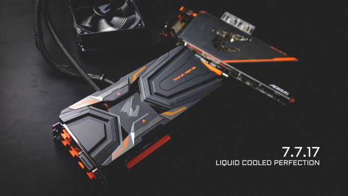
Both verbosely-named cards, as the Waterforce branding implies, are liquid-cooling oriented. The standard Waterforce Xtreme Edition is coupled with an all-in-one (AIO) closed loop cooler, while the Waterforce WB Xtreme Edition is outfitted with a full-size water block that can connect to a custom open loop. And so, without pesky fans taking up space, AORUS has dedicated the extra real estate on the card shrouds to a bountiful number of LEDs.
AORUS GeForce GTX 1080 Ti Waterforce Xtreme Editions 11G Waterforce Xtreme Edition Waterforce WB Xtreme Edition Boost Clock 1746MHz (OC Mode)
1721MHz (Gaming Mode)Base Clock 1632MHz (OC Mode)
1607MHz (Gaming Mode)Memory Clock 11448MHz (OC Mode)
11232MHz (Gaming Mode)VRAM 11GB GDDR5X
(352-bit)TDP Unspecified Outputs 3x DP1.4, 2x HDMI2.0b (Rear), 1x HDMI2.0b (Front) 1x DL-DVI-D
VR Link VR Mode: 3x DP1.4, 3x HDMI2.0b
VR Link Standard Mode: 3x DP1.4, 1x HDMI2.0b (Rear), 1x DL-DVI-DPower Connectors 2 x 8pin Length 267mm Width 2 Slot (36mm) 2 Slot (28mm) Height 123mm 149mm Cooler Type AIO CLC (120mm) Water Block (full-cover) Price TBA Generally speaking, both cards only differ in their cooling designs, having the same clocks, 12+2 power phases, and basic features. The 120mm AIO Waterforce Xtreme Edition has a water block that only covers the GPU, with a water block-cooled copper heatpipe and base plate covering the MOSFETs and VRAM. Behind the GPU, the card has a small copper piece embedded in the back plate. In comparison, the Waterforce WB Xtreme Edition has its water block and flow design covering all key components, and has a larger copper slab in the back plate.
Both cards offer the AORUS VR Link design for their display outputs. What this means is that an extra HDMI port is offered on the front (internal) side of the card, while the PCIe bracket has 2 HDMI ports, a DVI-D port, and 3 DisplayPorts. Due to the limited number of display controllers on the GP102 GPU, only 4 ports/displays can be used at one time. In standard mode, a maximum of 4 outputs can be used, selecting from among the first HDMI port, 3 DisplayPorts, and the DVI-D port on the PCIe bracket. In VR Mode, the DVI-D port is not used, and a maximum of 4 outputs can be used from among the 3 DisplayPorts and 3 HDMI ports. Ultimately, the idea is here that the front-facing HDMI can be used for a VR headset, while the rear HDMIs can still be utilized simultaneously for monitors without swapping cables.
As Xtreme Edition cards, the Waterforce and Waterforce WB qualify for an extra year of AORUS Care upon registration within 30 days of purchase, which then adds to AORUS’ standard three-year warranty for four total years. All-in-all, that could mean over 1400 days of guaranteed brightly-lit gaming sessions with RGB Fusion, AORUS’ LED software. For the WB variant, this includes lighting up the water block fittings and the AORUS eagle emblems on both sides of the card, giving the impression that AORUS has simply opted to create a giant rectangular LED that also happens to run games.

GIGABYTE has not announced pricing information at this time. A teaser posted by the official AORUS Twitter states 7/7/17, presumably the availability date for both cards.
More...
-
06-30-17, 12:18 PM #7129
Anandtech: The Enermax Revolution SFX 650W PSU Review: Compact & Capable
High performance SFX PSUs are gaining ground on the market and Enermax joins the train with the Revolution SFX series. The Revolution SFX units are modular, 80Plus Gold certified and boasting impressive performance specifications that rival these of current ATX designs. The Revolution SFX units are available in just two variations, the ERV550SWT and the ERV650SWT, and we are having a close look at the more powerful 650W version in this review.
More...
-
07-03-17, 07:48 AM #7130
Anandtech: LGs 34UC89G 21:9 Curved Display with G-Sync, 144 to 166 Hz, Available for
LG has begun to sell its new ultra-wide curved display that appears to be its first monitor to support NVIDIA’s G-Sync technology. The LG 34UC89G resembles the 34UC79G display launched almost a year ago — it has a 21:9 aspect ratio, a 2560×1080 resolution and a native maximum refresh rate of 144 Hz. However, the new unit has a number of important differentiators when compared to the 34UC79G: its panel is listed as brighter, it can be overclocked, and it features G-SYNC. It also costs $300 more.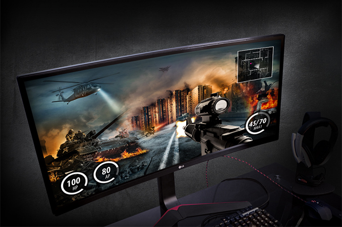
LG was an early adopter of AMD’s FreeSync back in early 2015 and since then it has launched numerous gaming displays featuring this technology. By contrast, the company has never released a monitor with NVIDIA’s G-Sync for an unknown reason. This summer LG finally decided to produce a G-Sync display and started with a model that has moderate characteristics by today’s standards. The LG UltraWide 34UC89G is outfitted with an IPS panel with a resolution of 2560×1080, a peak brightness of 300 nits, a contrast ratio of 1000:1, a 5ms GtG response time and 178° viewing angles. The panel has a native refresh rate of 144 Hz that can potentially be overclocked to 166 Hz, but that is not guaranteed. The new monitor looks like a re-engineered version of the 34UC79G, but given the fact that it has a different scaler (to enable G-Sync) and a panel that is 50 nits brighter and 166 Hz-capable, it seems to be a new display that shares chassis with one of its predecessors.
When it comes to connectivity, the LG UltraWide 34UC89G has a DisplayPort 1.2 and an HDMI 1.4 input, a dual-port USB 3.0 hub as well as a 3.5-mm audio jack. In some regions, the monitor may be equipped with two 7 W speakers (like the 34UC79G in Germany), but LG’s U.S. website does not mention them.
When LG released its 34UC79G last September, the combination of its features (IPS, curvature, a 144 Hz refresh rate and an ultra-wide aspect ratio) looked very compelling at a $699 price point. The situation is a bit different with the 34UC89G. The new monitor has the same 2560×1080 resolution and it costs $999.99 (likely due to G-Sync plus other factors). In the meantime, there is the Acer Predator Z35P 35” curved VA display offering a 3440×1440 resolution, a maximum refresh rate of 120 Hz (albeit via overclocking) and G-Sync available for $1099.99. The 34UC89G still has advantages - an IPS panel and a higher refresh rate.LG UltraWide 34UC89G Panel 34" IPS Native Resolution 2560 × 1080 Refresh Rate 144 Hz
Overclockable to 166 HzDynamic Refresh Rate Technology NVIDIA G-Sync
exact refresh rate range is unknownResponse Time 5 ms gray-to-gray Brightness 300 cd/m² Contrast 1000:1 Viewing Angles 178°/178° horizontal/vertical Pixel Pitch 0.312 mm × 0.31 mm Curvature 3800R (?) Anti-Glare Coating Yes, 3H Inputs DisplayPort 1.2 for 2560×1080 at 144-166 Hz
HDMI 1.4 for 2560×1080 at 60 HzUSB Hub 2-port USB 3.0 hub: two USB-A ports
one supports fast chargingAudio 3.5 mm audio jack
7 W × 2 (?)Launch Price $999
The LG UltraWide 34UC89G is now available from various retailers worldwide, including Amazon and Newegg in the U.S.
Gallery: LG UltraWide 34UC89G


Related Reading:
- LG Announces the 34UC79G: 34-Inch Curved 21:9 Display with 2560 × 1080 Resolution, 144 Hz Refresh Rate for $700
- AOC Launches the AG352QCX: 35-Inch 200 Hz 2560×1080 Curved Display with Adaptive-Sync
- Acer Predator X35 & ASUS ROG Swift PG35VQ Unveiled: 35-inch G-SYNC HDR Monitors - UltraWide, Curved, 200Hz
- Acer Predator Z35P Available for Order: Curved 35" with 3440×1440@120 Hz and G-Sync
- AOC Expands AGON Family with Curved AG322QCX and AG272FCX 144 Hz Displays
- AOC Announces the AGON AG352UCG 21:9 Curved Display: 35", 3440×1440, 100Hz with G-Sync
- HP Announces Omen X 35-Inch Curved Display for Gamers
More...


 Quote
Quote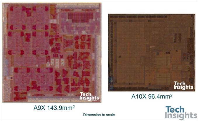
Thread Information
Users Browsing this Thread
There are currently 11 users browsing this thread. (0 members and 11 guests)


Bookmarks