

Results 7,231 to 7,240 of 12096
Thread: Anandtech News
-
08-14-17, 08:00 AM #7231
Anandtech: Shuttles X1 Now Available: NUC-Like PC With a GeForce GTX 1060 GPU
Shuttle has started to sell its new Gaming Nano family of small form-factor PCs. The miniature Shuttle X1 systems are barely larger than Intel’s NUCs, but they integrate Intel’s 45W high-end mobile Core i5/i7 HQ-series Kaby Lake CPUs with NVIDIA’s mobile GeForce GTX 1060 3 GB GPUs, which make them capable of running VR games. The combination of size and hardware leads to pricing from $1465 to $1709.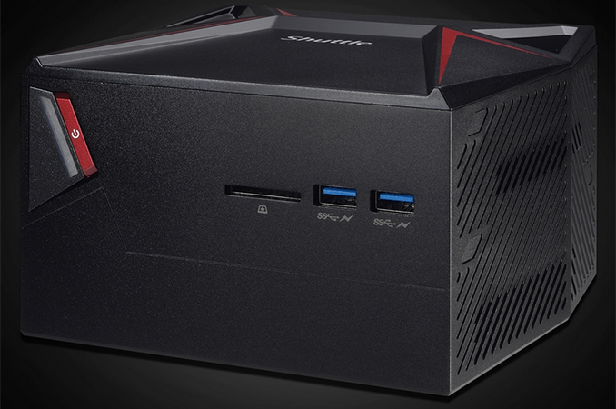
Shuttle and Mini PCs
Shuttle was among the pioneers of modern small form-factor PCs for enthusiasts in the early 2000s. Back then, the company was the first to offer custom PC barebones that enabled users to build a PC without hassle on motherboard fitting and cooling. Shortly after, the company began to offer specialized versions of PC barebones designed for HTPC and gaming applications, essentially pioneering SFF gaming PCs. Shuttle was among the first PC makers who offered cube-sized (somewhere between ITX and mATX) PCs based on Intel’s X58 and X79, inventing a miniature enthusiast PC category (over two years before Falcon Northwest’s Tiki) and showing a new market for boutique PC makers, and eventually manufacturers of PC components. Intensified competition and other issues eventually forced Shuttle to focus on non-gaming specialized PCs and barebones for several years, but it looks like the company is plotting a comeback. Earlier this year Shuttle launched its SZ270R8 barebones, based on the Intel Z270 chipset and aimed it at the audience that buys Mini-ITX PCs. In June, the company formally announced the first member of the Gaming Nano family — the Shuttle X1, which is aimed at a slightly less crowded market of miniature gaming systems.
The Shuttle X1
The Shuttle X1 is an extremely small desktop PC that fits in a palm of a hand and resembles higher-end Intel NUC computers and competitors. Just like the NUC, the Shuttle X1 is based on Intel’s mobile CPUs, going up to 45W versions of the Core i5-7300HQ and Core i7-7700 HQ. But unlike Intel's NUCs, the X1 also carries an NVIDIA GeForce GTX 1060 3GB MXM GPU module. The systems are equipped with 8 GB or 16 GB of DDR4 memory operating in dual-channel mode. As for storage, the entry-level X1 has a 128 GB M.2 SSD and a 1 TB HDD, whereas the more advanced X1 PCs feature 256 GB M.2 drives without HDDs.
When it comes to connectivity, the Shuttle X1 offer a rather typical set of I/O features, including 802.11ac Wi-Fi + Bluetooth, a GbE port, one USB 3.0 Type-C connector, four USB 3.0 Type-A headers (two on the front), four USB 2.0 ports, three HDMI outputs (one for a VR headset), one DisplayPort, one SD card reader as well as one 3.5-mm audio jack.
*For the GTX 1060, the desktop GPUs have different specifications for the 6GB (1280 cores) compared to the 3GB (1152 cores). The laptop versions of the GTX 1060 do not make this distinction - all the cards have 1280 cores, and there is no 1152 core variant for MXM.Shuttle X1 Specifications Model Shuttle X1 i7 Shuttle X1 i5 Pro Shuttle X1 i5 CPU Core i7 7700HQ
4C/8T
2.8/3.8 GHz
6 MB cache
45 W TDPCore i5 7300HQ
4C/4T
2.5/3.5 GHz
6 MB cache
45 W TDPGPU GeForce GTX 1060 with 3 GB of GDDR5 memory
1280 CUDA Cores, 80W TDP*DRAM 16 GB DDR4-?
Dual Channel8 GB DDR4-?
? ChannelUpgradeable to 32 GB Motherboard Custom Storage SSD 128 GB M.2 256 GB M.2 HDD 1 TB HDD - Wireless 802.11ac Wi-Fi + Bluetooth
Intel AC (8265?)Ethernet 1 GbE port USB 1×USB 3.0 Type-C
4×USB 3.0 Type-A
2×USB 1.0 Type-ADisplay Outputs 1×DisplayPort
3×HDMIAudio 1×3.5mm audio jack Card Reader SD card reader PSU external Warranty 3 years Dimensions Not Specified, but 'shorter than a soda can' MSRP with Launch Discount $1709 $1500 $1465
The Shuttle X1 chassis has a rather aggressive design with red elements and an unorthodox shape. A good thing about small dimensions is that the Shuttle X1 is easy to carry. A bad thing about the X1 is that it uses a number of custom components (chassis, motherboard, cooling, etc.) as well as mobile CPUs and GPUs, all of which are relatively expensive. As a result, the most affordable Shuttle X1 costs $1465 even with a discount, whereas the most advanced one is sold for $1709. All three Shuttle X1 systems are now available directly from the company and usually ship in one or two business days.
Related Reading:
- Corsair’s ONE SFF PCs Get Upgraded: GeForce GTX 1080 Ti, 32 GB of RAM, NVMe SSD
- Zotac Unveils 2017 ZBox Magnus SFF Gaming PCs: Powered By Intel Core & AMD Ryzen
- ASUS VivoPC X Console Now Available: Core i5, GeForce GTX 1060 for $799
- MSI Upgrades Its Aegis and Nightblade PCs with Intel’s Kaby Lake CPUs
- MSI Trident 3 Announced: A Core i7 Console
- GIGABYTE's New Console: The 'Gaming GT' PC Launched with Core i7-K, GTX1080, TB3
- Corsair’s Bulldog 2.0 Gets Kaby Lake-Compatible Z270 Motherboard, New Cooler
More...
-
08-14-17, 09:20 AM #7232
Anandtech: The AMD Radeon RX Vega 64 & RX Vega 56 Review: Vega Burning Bright
We’ve seen the architecture. We’ve seen the teasers. We’ve seen the Frontier. And we’ve seen the specifications. Now the end game for AMD’s Radeon RX Vega release is finally upon us: the actual launch of the hardware. Today is AMD’s moment to shine, as for the first time in over a year, they are back in the high-end video card market. And whether their drip feeding marketing strategy has ultimately succeeded in building up consumer hype or burnt everyone out prematurely, I think it’s safe to say that everyone is eager to see what AMD can do with their best foot forward on the GPU front.
Launching today is the AMD Radeon RX Vega 64, or just Vega 64 for short. Based on a fully enabled Vega 10 GPU, the Vega 64 will come in two physical variants: air cooled and liquid cooled. The air cooled card is your traditional blower-based design, and depending on the specific SKU, is either available in AMD’s traditional RX-style shroud, or a brushed-aluminum shroud for the aptly named Limited Edition.
More...
-
08-14-17, 10:18 AM #7233
Anandtech: Arctic Announces the Freezer 33 TR: An Air Cooler Designed for AMDs Threa
Arctic has announced a special version of its popular Freezer 33-series cooler, this time designed specifically for AMD’s Ryzen Threadripper microprocessor. The cooler is not only physically compatible with the Socket TR4 mounting mechanism, but the base has been extended to cover Threadripper’s integrated heatspreader (IHS) in order to improve cooling efficiency.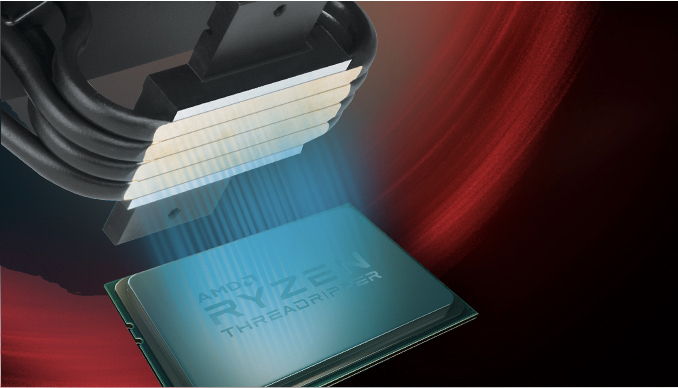
The MCM architecture of AMD’s EPYC and Threadripper processors required AMD to design a CPU form-factor and socket that is explicitly rectangular rather than square-like. Since AMD’s Socket TR4 for the Threadripper CPUs derives from the Socket SP3r2 for servers, it has the same shape and dimensions. Most of the coolers on the market today were not designed for such a large rectangular contact like TR4 and they cannot cover 100% of its surface because they were developed for square-like CPUs. So while it is possible to use an existing cooler for AMD’s TR4 CPUs using special mounting brackets, its base does not cover part of the IHS and this is potentially going to lower its efficiency - cooling companies are now moving forward with larger TR4 specific designs to address this market.
The Freezer 33 is currently the flagship air CPU cooler from Arctic. The device has four 6-mm copper heatpipes, 49 aluminum fins that are 0.4-mm thick, and a 120-mm fan. The main difference between the new Freezer 33 TR versus the regular Freezer 33 is a slightly longer copper base, as well as the black and red color scheme (black and white scheme is also available). Other than that, everything is the same. By redesigning the base of its Freezer 33 TR cooler for the sTR4, Arctic is aiming to enhance its thermal performance for AMD's new CPUs and potentially give some additional overclocking headroom for those who need it.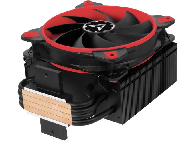
Arctic claims that the Freezer 33 TR was developed to cool down CPUs with up to 200 W TDP, but its maximum cooling capacity is 320 W. The design of the cooler can support the installation of two fans (to maximize potential) as well as supporting the installation of memory modules of moderate height. Arctic’s fans for the Freezer 33 TR use fluid dynamic bearing motors, feature 200-1800 RPM speed and are PWM-controlled to minimize noise under light loads.
The redesign of the base of the cooler has affected the compatibility of the Freezer 33 TR cooler with mainstream Intel platforms. The new cooler is thus only compatible only with AMD’s TR4 and AM4, as well as Intel’s LGA2011-3 as well as LGA2066 sockets.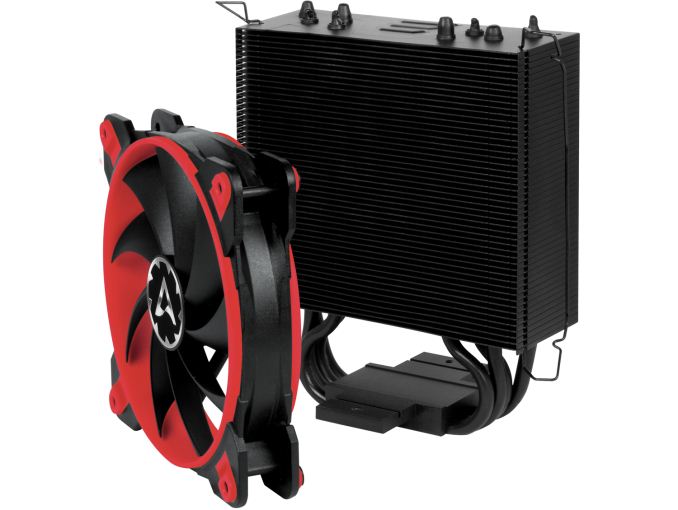
The Arctic Freezer 33 TR is already available directly from the company and its resellers are set to get the cooler in the coming days or weeks. The product costs €47.99 and will be one the most affordable coolers designed specifically for AMD’s Ryzen Threadripper.
Gallery: Arctic Announces Freezer 33 TR: An Air Cooler Designed for AMDs Threadripper


Related Reading- Enermax Launches LiqTech TR4 AIO LCS for AMD's Threadripper: 100% IHS Coverage, 500 W TDP
- G.Skill Unwraps Flare X 32 GB and 128 GB DDR4 Kits for AMD Threadripper: Up to 3600 MT/s
- The AMD Ryzen Threadripper 1950X and 1920X Review: CPUs on Steroids
- Unannounced AMD Ryzen Threadripper 1920 CPU in Motherboard Support Lists
- Patriot Publishes List of AMD Ryzen Compatible DIMMs: Up to DDR4-3400, 64 GB
- AMD Announces Ryzen AGESA 1.0.0.6 Update: Enables Memory Clocks Up To DDR4-4000
More...
-
08-14-17, 01:25 PM #7234
Anandtech: EKWB Unveils Threadripper Edition EK Supremacy EVO CPU Water Blocks
Since Threadripper was first spotted in the wild, enthusiasts interested in the CPU noticed just how big the CPU actually was. For the past several CPU generations, the size of the integrated heat spreader (IHS) on high-end platforms has not changed too much from either Intel nor AMD. Threadripper, however, is a game changer. It is nearly twice the size of an Intel LGA2066 CPU, and that much larger surface area is expected to have heatsink contact across the entire IHS for the best cooling results out of anything trying to cool it. A concern comes with existing heatsinks and their now diminutive base plates; they don’t cover the entire IHS. Heatsink and water-block makers are forced to update their designs or face potentially underwhelming performance due to the lack of complete coverage. EKWB has thus announced its new EK-Supremacy EVO Threadripper Edition CPU water block which covers the entire IHS.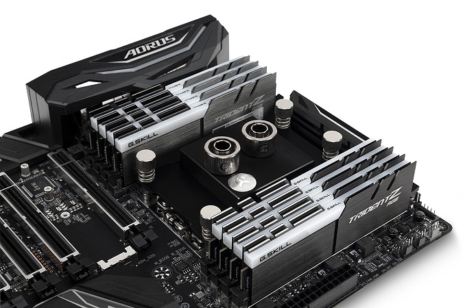
EK has redesigned the nickel plated machined copper base for a length of 68mm, which is up 10mm from the original Supremacy EVO. This small bump in size enables the cold plate to have complete coverage over the IHS. The Threadripper Edition Supremacy EVO comes pre-assembled and installs directly onto SocketTR4 motherboards, and is screwed down to the mounting holes surrounding the even bigger socket where Threadripper sits. As the block fits in the TR4 mounting holes, it should also compatible with AMD server socket SP3r2 motherboards.
The TR Edition Supremacy EVO uses the EK-Supremacy EVO cooling engine, consisting of a specialized jet insert and jet plate combination. The water goes in through a standard G ¼” barb to the jet plate, then through a 52 groove micro-fin base (each 0.25mm apart). EKWB says the fins are oriented so the water inside the block is pushed up and down towards the CPU dies under the IHS.
EK Supremacy EVO Threadripper Edition has three different versions; Nickel, Acetal+Nickel, and Full Nickel. All three versions use a black steel mounting plate, with the thumb screws pre-installed, integrated into the block. The Nickel and Nickel+Acetal edition tops are CNC machined from POM high-grade acrylic glass. The 'plain' nickel version is transparent while the Nickel+Acetal has a black nickel coating around the acetal block top. The Full Nickel option is also CNC machined, but using nickel-plated brass as the base material. EK uses a pre-installed molded ABD polymer insert on all versions to 'ensure the optimal flow of water' through the block.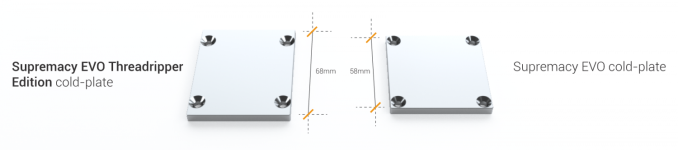
Prices range from $77.99 for the Nickel and Acetal+Nickel blocks to $99.99 for the Full Nickel.


The Supremacy EVO Threadripper Edition is available now for pre-order at the EKWB site. Shipments are expected to start on August 18th.EK Supremacy EVO Threadripper Edition MSRP (incl. VAT) EK-Supremacy EVO Threadipper Edition - Nickel 67.95€ EK-Supremacy EVO Threadipper Edition - Acetal+Nickel67.95€ EK-Supremacy EVO Threadipper Edition - Full Nickel86.95€
Gallery: EKWB Supremacy EVO Threadripper Edition


Related Reading- The AMD Ryzen Threadripper 1950X and 1920X Review: CPUs on Steroids
- Unannounced AMD Ryzen Threadripper 1920 CPU in Motherboard Support Lists
- Enermax Launches LiqTech TR4 AIO LCS for AMD's Threadripper: 100% IHS Coverage, 500W TDP
- AMD Threadripper 1920X and 1950X CPU Details: 12/16 Cores, 4 GHz Turbo, $799 and $999
More...
-
08-14-17, 03:36 PM #7235
Anandtech: EVGA Launches SC17 1080 Laptop: Core i7-7820HK, GeForce GTX 1080, TB3
EVGA has launched its new flagship 17.3” laptop with a new CPU, a new GPU, and with Thunderbolt 3 support. The new SC17 1080 gaming notebook is thicker than its predecessors, but it features higher performance due to Intel’s latest Core i7-7820HK mobile CPU as well as NVIDIA’s flagship GeForce GTX 1080 graphics processor for laptops. Just like predecessors, the SC17 has a 4K display and allows its owners to overclock the CPU.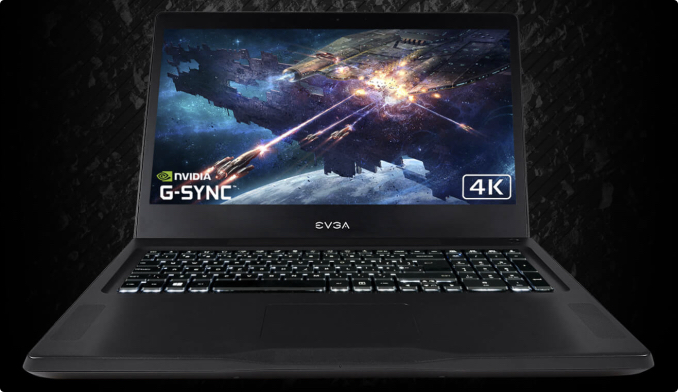
EVGA introduced its first SC17 notebook in March 2016 with an aim to offer desktop-class performance and feature set in a clamshell chassis that is 1.05” (26.9 mm) thick: a 4K (3840×2160) display, an overclockable CPU, 32 GB of memory and a rather advanced storage sub-system are meant to serve this purpose. Earlier this year EVGA launched a new version of the SC17 with NVIDIA’s GeForce GTX 1070 GPU, bringing the performance of the system on par with other contemporary gaming laptops. This month, the company decided to increase the performance of its flagship notebook further and in a bid to do that, it had to introduce new chassis. The SC17 1080 laptop is 1.3” (30 mm) thick, but its weight is still around 4 kilograms, in line with many 17”-class gaming machines. The new enclosure enabled EVGA to equip the SC17 1080 with a new cooling system that can handle Intel’s new Core i7-7820HK CPU based on the Kaby Lake microarchitecture (4C/8T, 2.9G-3.90G) and NVIDIA’s GeForce GTX 1080 mobile GPU (2560 stream processors, 160 texture units, 64 ROPs) with 8 GB of GDDR5X memory. In addition, the flagship laptop now features a Thunderbolt 3 port to connect the system to various high-performance peripherals (such as external storage or displays).
Apart from the upgraded CPU and GPU, the new SC17 1080 has the same features and configuration as the original: it is equipped with 32 GB of G.Skill’s DDR4-2666 memory, a 256 GB M.2 NVMe SSD (PCIe 3.0 x4 interface) and a 1 TB hard drive with 7200 RPM spindle speed. When it comes to connectivity, the SC17 1080 is almost identical to its predecessors: it has an 802.11ac Wi-Fi + Bluetooth 4.2 module, a gigabit ethernet RJ-45 connector, one Thunderbolt 3/USB 3.1 Type-C port, three USB-A 3.0 ports, two mDP headers, an HDMI output, an FHD webcam and so on. Just like on the previous SC17 models, the SC17 1080 allows the user to fine-tune CPU voltages in a bid to maximize overclocking potential, as well as to overclock the GPU. If something goes wrong, there is a CMOS clear button on the chassis.
By making its SC17 1080 thicker than its predecessors, EVGA is going against the industry's recent trend to make gaming laptops thinner. EVGA's rivals Acer and ASUS have embraced NVIDIA's MaxQ initiative that enables notebook manufacturers to make their GeForce GTX 1080-based PCs thinner and lighter at the expense of performance in games (which is still very high, especially for a mobile PC). By contrast, EVGA wants its SC17 1080 to offer the highest performance possible (but without going extreme with add-on liquid cooling, etc.) and have an additional overclocking headroom both for the CPU and GPU.
The new EVGA SC17 1080 laptop is not only thicker and faster than its predecessors, but it is also more expensive too due to the updates. The new gaming laptop costs $2999.99, up from $2549.99 for the SC17 1070.
Related Reading- EVGA Rolls Out SC17: High-End Gaming Laptop Designed for Overclocking
- EVGA Introduces the GTX 1080 Ti K|NGP|N Edition Video Card
- EVGA's New iCX Range: NVIDIA GPUs with More Control for Cooling
- Acer Announces Predator Triton 700 Gaming Laptop: Core i7, GeForce GTX 10 Series, & 1 TB SSD
- Acer Announces The Acer Predator 21 X: 21-Inch Curved Screen Gaming Notebook
- Razer Blade Gets Core i7-7700HQ, Adds 4K Touchscreen, 1 TB SSD Options
- Razer Re-Launches The Razer Blade Pro: GTX 1080 And 4K G-SYNC
- Dell Readies New XPS 15: 4K, Quad-Core Kaby Lake, GeForce GTX 1050
- The ASUS ROG Strix GL502VS Review: Mainstream GTX 1070 with G-SYNC
More...
-
08-15-17, 04:08 AM #7236
Anandtech: More Denverton Noise: GIGABYTEs MA10-ST0 Features Unannounced 16-Core C39
Today GIGABYTE Server (the server arm of GIGABYTE, a different BU to the motherboard team) has lifted the lid on their new MA10-ST0 motherboard and SoC combination, aimed squarely at the cold storage or edge storage market. This includes base support for up to 16 SATA drives via SFF8087, a PCIe x8 slot, 10 gigabit Ethernet via two SFP+ ports, and server management features via the Aspeed AST2400. For server/enterprise features, a TPM header and a COM header are also present. The interesting twist in this tale, however, is the SoC at the heart of the unit.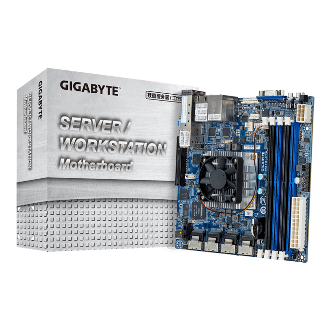
GIGABYTE Server has announced they are using the C3958 SoC, listed as a 16-core part at 31W TDP and supporting DDR4-2400. The C3000 series is known as the Denverton family of CPUs, based on Intel’s Goldmont Atom microarchitecture. The Denverton CPU family has been formally announced, although only as a single SKU, the dual core C3338, which is present in some enterprise NAS devices. Some others have cited cloud instances featuring unannounced Denverton CPUs being deployed and available by cloud providers. This C3958 is another unannounced processor from Intel.
Intel’s Atom line in this market is still recovering from the Avoton/Rangeley issue that cropped up 18-24 months after launch, which had an outside chance of burning out the signal generator resulting in a system that would be unable to be repaired (we are told that an unusual spike in failures is not expected from this, but for users who deploy 10-15 year embedded devices it might be in the back of their minds). From this, Intel released a new stepping of the CPU to address the bug, and some have predicted that the delays to the formal announcement and release of the Denverton stack (some 12 months or more after the expected announcement date) is due to ensuring Denverton does not have this issue.
As for the C3958, GIGABYTE Server lists this as Intel’s top Denverton SoC model, running at 16 cores, 1MB of L2 per core, 2.0 GHz base frequency (no word on turbo), support for up to 128GB of DDR4-2400 RDIMMs (or 64GB of UDIMMs, i.e. 4x16GB modules) and having a 31W TDP. Typically around this SoC level, we might expect to compare it to an E3-1200 v6 series processor, although those CPUs start at 72W. The previous generation Rangeley processor topped out at 8 cores and 2.4 GHz for 20W, so on paper there looks to be some efficiency gain despite the frequency decrease.
As for the MA10-ST0 motherboard, along with all the features above it also comes with 32GB of eMMC flash, allowing a user to install a storage-based OS for a network deployment without using any of the onboard SATA ports. GIGABYTE Server has told us that board is essentially ready to go, and interested parties should get in contact with their local reps.
Related Reading
- Semi-Critical Intel Atom C2000 SoC Flaw Discovered, Hardware Fix Required
- Intel Announces Atom E3900 Series - Goldmont for the Internet of Things & More
- Intel Quietly Launches Apollo Lake SoC: Goldmont CPU, 6 SKUs, 6 & 10 Watts
- Spot The Denverton: Atom C3000 Silicon On Display
More...
-
08-15-17, 07:46 AM #7237
Anandtech: Geil Announces EVO Spear Series DRAM: Up to DDR4-3466
Geil recently announced the availability of its new EVO Spear series of memory, with kits labeled specifically for either Intel and AMD Ryzen based systems. Geil states the EVO Spear series is intended for gamers, enthusiasts, and case modders looking for a cost-effective upgrade. The two flavors give one for Intel and the other for AMD Ryzen with capacities up to 64GB and speeds reaching 3600 MT/s (although not at the same time).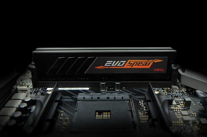
Geil says the EVO Spear series of RAM is optimized for Intel Core X, i7, and i5 Processors which includes the Z200 and X299 series chipsets. They go on to say the AMD Edition sticks are fully compatible with Ryzen 7, Ryzen 5 Processors, and AM4 motherboards, and we suspect that Ryzen 3 and Threadripper will be supported eventually as well. The only differences between the two versions are the QVL and compatibility testing - while most kits should work in most boards, the AMD kits are officially certified in various AM4 boards and Intel kits for 200-series boards. The maximum speed on the AMD Edition kits top out a bit lower as well.
From Ryzen's release day, board partners have been working with AMD to further increase compatibility with AGESA updates via new BIOS, and the market is seeing more and more AMD compatible RAM at faster speeds as time goes on, so the updates are working. The AMD Edition sticks have an AMD Ryzen logo found on the packaging and modules, while the Intel sticks are nondescript.
Capacities range from 16GB up to 64GB in both dual and quad channel kits. The operating frequency for the Intel sets is up to 3466 MHz, while the AMD Edition peaks at 3200 MHz. CAS ratings will vary by SKU but range from CL15 to CL17m and Geil offers a limited lifetime warranty on the EVO Spear Gaming Memory.


The DIMMs use standard height heat sinks ensuring “zero mechanical interference” from the sticks. They are available only in a stealth black heat colored spreader with the EVO Spear name on the side. The heat spreader covers a black PCB, and in an effort to remain cost effective, RGB LEDs are not on the EVO Spear line.

 In total there are over 50 different kits coming to market, divided by capacity (2x4 GB, 2x8 GB, 2x16 GB, 4x4GB, 4x8GB, 4x16GB) - the Geil website has the details. Pricing was not listed, however, a couple of dual channel kits are already available on newegg.com. A 2x8GB DDR4-2400 CL16-16-16-36 AMD Edition kit sells for $130.99 and a 2x8GB DDR4-2800 CL16-16-16-36 kit is asking $135.99.
Geil EVO Spear DRAM Latency Voltage Max Size Intel SKU AMD
SKUDDR4-2133 15-15-15-36 1.2 V 4x 16GB GSB464GB2133C15QC DDR4-2400 15-15-15-36 1.2 V 4x 16GB GSB464GB2400C15QC 16-16-16-36 GSB464GB2400C16QC 17-17-17-39 GSB464GB2400C17QC DDR4-2666 16-18-18-36 1.35 V 4x 16 GB GSB464GB2666C16AQC DDR4-2800 16-16-16-36 4x 16 GB GSB464GB2800C16QC DDR4-3000 16-18-18-36 4x 16 GB GSB464GB3000C16AQC DDR4-3200 16-18-18-36 4x 8 GB GSB432GB3200C16AQC DDR4-3466 16-18-18-38 4x 8 GB GSB432GB3466C16QC -
Related Reading:- The AMD Zen and Ryzen 7 Review: A Deep Dive on 1800X, 1700X, and 1700
- The AMD Ryzen Threadripper 1950X and 1920X Review: CPUs on Steroids
- The Intel Skylake-X Review: Core i9 7900X, i7 7820X, and i7 7800X Tested
- AMD Announces Ryzen AGESA 1.0.0.65 Update: Enables Memory Clocks Up To DDR4-4000
- Patriot Publishes List of AMD Ryzen Compatible DIMMs: Up to DDR4-3400, 64GB
More...
-
08-15-17, 07:46 AM #7238
Anandtech: Seagate Demos New SSD Features And Prototypes At FMS
In spite of a fire that closed the exhibition floor last week at Flash Memory Summit, Seagate managed to set up several live demos and display their latest SSDs along with a few prototypes, all in a meeting room safely away from the ruined exhibits.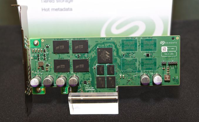
We've previously covered the new products Seagate announced at the beginning of the show last week. Pictures of the Nytro 5000 M.2 SSD, the 15TB Nytro 3000 series SAS SSD, and the 64TB demo based on eight M.2 SSDs are all in the gallery below.
Live Demos
The two live demos used what appeared to be Nytro XP7102 SSDs in the half-height half-length add-in card form factor, but with Micron 3D NAND instead of the planar MLC that the XP7102 launched with. These drives use the same Marvell 88SS1093 controller that is in the Nytro 5000 and in several consumer SSDs. The live demos showed that Seagate has implemented support for the Streams feature from the NVMe 1.3 specification, and IO determinism which has been approved for the next revision of the NVMe specification.
The Streams demo illustrated how tagging write operations according to which task they belong to allows the SSD to keep related writes together and put unrelated data in separate erase blocks. When used properly, data from the same stream can be expected to have a similar lifetime, so when part of it gets invalidated or overwritten, everything in that erase block will also soon be available for garbage collection. With the longer-lived data stored elsewhere, the SSD has far less data to move and compact during its garbage collection process, which leads to lower write amplification and improved performance. For the test scenario Seagate concocted, they were able to show write amplification being reduced from around 8.6-9 down to about 1.03, while throughput for the worker thread that was shown on screen improved from around 9.7k IOPS to 83k IOPS.
The new NVMe IO Determinism feature serves a similar purpose, but implements it in a very different way. NVMe Streams directives are essentially hints to the SSD controller about how to physically organize data. The IO Determinism feature asks the SSD to make hard guarantees by dividing its flash chips and channels into separate NVM Sets. IO to one set will never block access to another set because the data resides on different physical chips. Saturating the PCIe link or overloading the controller's available CPU power would be the only ways for one task to degrade another's IO performance. The downside to this static partitioning method is that a single task accessing one NVM Set will not be able to use the full performance or capacity of the drive, even if there are no other tasks accessing the drive.
The IO Determinism feature also provides for timeslicing access to the SSD, where the drive can provide a window for deterministic IO where background garbage collection is suspended, followed by a non-deterministic period where normal access is permitted by performance may be degraded as the garbage collector catches up. This is essentially a standardization of the "Host Managed SSD" feature OCZ implemented for its Saber 1000 enterprise SATA SSDs in 2015.
Prototypes
Seagate also showed off two unannounced prototypes that they had not planned to feature at their booth. The first was dubbed the Nytron 5000B, a variant of the Nytro 5000 M.2 SSD that is intended as a high-performance boot drive. This was commissioned by a large customer that did not wish to be named. The drive included 256GB of 3D MLC NAND and 2GB of DRAM, plus a connection to an external pack of capacitors. With such a large bank of capacitors, the 5000B can be far more aggressive about caching both metadata and user data in DRAM, allowing for burst write performance far in excess of what the flash could sustain, and without compromising data safety.
The other prototype had similar aims, but instead of a capacitor-backed bank of DRAM it featured 128MB of Everspin STT-MRAM in addition to a normal DRAM cache for metadata. Seagate envisions using the MRAM either as a write cache for user data, or exposing it directly as a separate storage namespace for explicit tiered storage. This MRAM prototype drive was not a preview of an upcoming product. Instead, Seagate views this as a test platform to explore the possibilities and performance characteristics of MRAM, now that it is available in useful capacities.
Gallery: Seagate Demos at FMS 2017


More...
-
08-15-17, 09:38 AM #7239
Anandtech: Samsung Portable SSD T5 Review: 64-Layer V-NAND Debuts in Retail
?Samsung has been an active participant in the high-performance external SSD market with their Portable SSD series. The T1 was introduced in early 2015, while the T3 came out in early 2016. The T3 was the first retail product to utilize Samsung's 48-layer TLC V-NAND. Today, Samsung is launching the Portable SSD T5. It is a retail pilot vehicle for their 64-layer TLC V-NAND as they ramp up its production. The Portable SSD T5 also moves up to a USB 3.1 Gen 2 Type-C interface, while retaining the same compact form factor and hardware encryption capabilities of the Portable SSD T3. Read on for our analysis of the product's performance and value proposition.
More...
-
08-15-17, 09:38 AM #7240
Anandtech: Intel Officially Reveals Post-8th Generation Core Architecture Code Name:
In an unusual move for Intel, the chip giant has ever so slightly taken the wraps off of one of their future generation Core architectures. Basic information on the Ice Lake architecture has been published over on Intel's codename decoder, officially confirming for the first time the existence of the architecture and that it will be made on Intel's 10nm+ process.
The Ice Lake processor family is a successor to the 8th generation Intel® Core™ processor family. These processors utilize Intel’s industry-leading 10 nm+ process technology.
This is an unexpected development as the company has yet to formally detail (let alone launch) the first 10nm Core architecture – Cannon Lake – and it's rare these days for Intel to talk more than a generation ahead in CPU architectures. Equally as interesting is the fact that Intel is calling Ice Lake the successor to their upcoming 8th generation Coffee Lake processors, which codename bingo aside, throws some confusion on where the 14nm Coffee Lake and 10nm Cannon Lake will eventually stand.
As a refresher, the last few generations of Core have been Sandy Bridge, Ivy Bridge, Broadwell, Haswell, Skylake, with Kaby Lake being the latest and was recently released at the top of the year. Kaby Lake is Intel’s third Core product produced using a 14nm lithography process, specifically the second-generation ’14 PLUS’ (or 14+) version of Intel's 14nm process.
Meanwhile when it comes to future products, back at CES Intel briefly showed a device based on post-Kaby Lake designs, called Cannon Lake and based on their 10nm process. Since then Intel has also confirmed that the 8th Generation of processors for desktops, called Coffee Lake, will be announced on August 21st (and we recently received promotional material to that effect). Ice Lake then, seems poised to follow both Coffee Lake and Cannon Lake, succeeding both architectures with a single architecture based on 10nm+.
Working purely on lithographic nomenclature, Intel has three processes on 14nm: 14, 14+, and 14++. As shown to everyone at Intel’s Technology Manufacturing Day a couple of months ago, these will be followed by a trio of 10nm processes: 10nm, 10nm+ (10+), and 10++,
On the desktop, Core processors will go from 14 to 14+ to 14++, such that we move from Skylake to Kaby Lake to Coffee Lake. On the Laptop side, this goes from 14 to 14+ to 14++/10, such that we move from Skylake to Kaby Lake to Coffee Lake like the desktops, but also that at some time during the Coffee Lake generation, Cannon Lake will also be launched for laptops. The next node for both after this is 10+, which will be helmed by the Ice Lake architecture.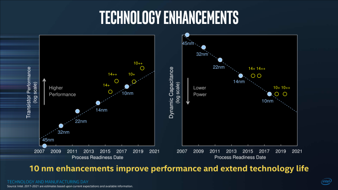
The way that the desktop and laptop markets will be diverging then converging is confusing a lot of people. Why is the laptop market splitting between 14++ and 10, and why is the desktop market not going to 10nm but straight to 10+? What lies beyond is a miasma of guess work, leaked slides, and guessing Intel’s strategy, but I believe the answer lies in Intel’s manufacturing technologies and the ability to move to newer lithographic nodes.Intel's Core Architecture Cadence Microarchitecture Core Generation Process Node Release Year Sandy Bridge 2nd 32nm 2011 Ivy Bridge 3rd 22nm 2012 Haswell 4th 22nm 2013 Broadwell 5th 14nm 2014 Skylake 6th 14nm 2015 Kaby Lake 7th 14nm+ 2016 Coffee Lake 8th 14nm++ 2017 Cannon Lake 8th? 10nm 2018? Ice Lake 9th? 10nm+ 2018?
(We should interject here that the naming of a lithographic node has slowly lost its relevance between the features of the process and the actual transistor density and performance, such that TSMC’s improved 16FF+ is called 12FFN, but relies on similar transistor sizes with enhanced attributes. But 12 is a smaller number than 14, which is the marketing angle kicking in. By all accounts, Intel has typically been considered the more accurate foundry when it comes to numerical lithographic naming of the process, which others consider is to their detriment.)
Intel originally predicted that they would move to 10nm almost a year ago, at the end of 2016 and 2 years after the launch of their 14nm process. But the challenge in managing the technology required to advance to their version of 10nm has been fraught with difficulty. In all cases it can depend on external equipment, fine tuning a process, or getting acceptable yields – while one manufacturer might be satisfied with an 80% yield, another might consider that a failure. Being able to obtain high yields (ramp up) will also be a function of die size, and so the newest nodes are typically launched with smaller mobile parts in mind first, as the yields for smaller parts are better than larger parts at the same defect rate.
Simply put, the first generation of 10nm requires small processors to ensure high yields. Intel seems to be putting the smaller die sizes (i.e. anything under 15W for a laptop) into the 10nm Cannon Lake bucket, while the larger 35W+ chips will be on 14++ Coffee Lake, a tried and tested sub-node for larger CPUs. While the desktop sits on 14++ for a bit longer, it gives time for Intel to further develop their 10nm fabrication abilities, leading to their 10+ process for larger chips by working their other large chip segments (FPGA, MIC) first.
From a manufacturing standpoint, Intel has been using multiple patterning techniques in its 14nm processes, and the industry is looking to when the transition to EUV will take place. Anton has some great writeups of the state of EUV and how different companies are transitioning to smaller nodes - they are well worth a read.
- EUV Lithography Makes Good Progress, Still Not Ready for Prime Time
- Samsung and TSMC Roadmaps: 8 and 6 nm Added, Looking at 22ULP and 12FFC
- GlobalFoundries Updates Roadmap: 7 nm in 2H 2018, EUV Sooner Than Later?
The crux of the matter is that EUV would shorten time to market and arguably make the process easier (if only more expensive), and several fab companies are waiting for Intel to jump onto it first. With EUV not ready, Intel has had to invest into deeper multi-patterning techniques, which raise costs, decrease yields, and increase wafer process times considerably.
All of which leads to a miasma of increased delays, much to the potential chagrin of investors but also customers who had banked on the power improvements that a typical new lithography node brings. Intel is still keeping spirits high, by producing numbers that would suggest that their methodology is still in tune with Moore’s Law, even if the products seem to be further strung out. Some analysts concur with Intel’s statements, while others see it as hand-waving until 10/10+ hits the market. Intel would also point out that it is developing other technologies such as Embedded Multi-Die Interconnect Bridges (EMIB) to assist in equipping chip with high-speed fabric or glue-logic.
Given its position as a post-8th gen architecture, Ice Lake is likely to hit sometime in 2018, perhaps 2019, depending on Intel’s rate of progress with larger chips and the 10+ process. Intel’s other market segments, such as FPGAs (Altera), Xeon Phi (MIC) and custom foundry partners, are also in the mix to get into some 10nm action.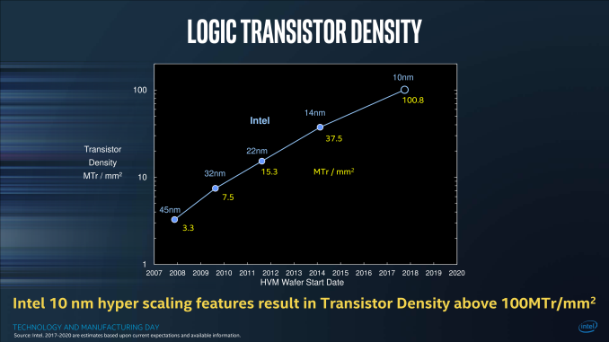
(Note that Intel’s next generation of Xeon Scalable Processors is called Cascade Lake, a 2018 refresh of the Skylake generation launched this year.)
Gallery: Intel Manufacturing Tech Day


More...


 Quote
QuoteThread Information
Users Browsing this Thread
There are currently 37 users browsing this thread. (0 members and 37 guests)


Bookmarks