

Results 7,361 to 7,370 of 12094
Thread: Anandtech News
-
09-20-17, 12:06 PM #7361
Anandtech: Kailh Introduces Low Profile Mini Chocolate Keyswitches
Mechanical keyboards have been a part of PC computing long before many of us were born and still have a place in the market today. With laptops becoming hugely popular in that time, many of the technologies found in full-sized PCs are making its way to the laptop space, including the mechanical keys many prefer to use due to the tactile and aural feedback. As time went on, technologies have improved and so have the number of choices consumers have in the mechanical keyboard space.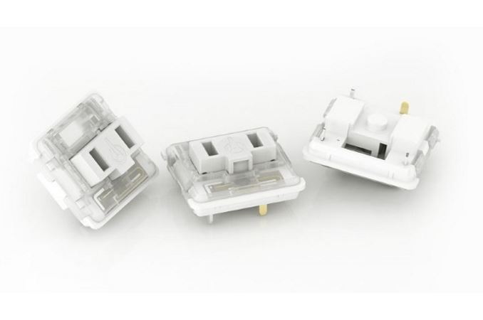
In the past, it was either Cherry MX or membrane-based keyboards. Today, however, the market has many switches offering a wide range of characteristics from multiple sources. One of the biggest challenges is trying to fit mechanical keys into smaller devices. In comes Kailh with its PG1232 Mini Chocolate mechanical keyswitch.
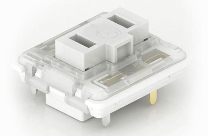
The PG1232 has a lower height than its regular mechanical switches and offers a pretravel of 1.2mm (±0.5mm) with an actuator/total travel of 2.4mm (±0.5mm). Compared to the original Chocolate key switches, which are set up with a total travel of 3mm and an actuation point at 1.5mm using 50g actuation force, this reduces the total travel height by 0.6mm (~ 20%). Meanwhile the PG1232 is also a bit smaller overall, measuring 14.5mm(W) x 13.5mm(D) x 8.2mm(H) versus the 15mm x 15mm x 11mm on the original chocolate key switches. This downsizing aims to make the switches more practical for use in laptop keyboards while still maintaining that tactile feel and aural feedback user want from a mechanical switch.
The White PG1232 switches are the ‘clicky’ type. There wasn't a mention of different types for the Mini, however, Kailh already has a presence in this space with its low-profile PG1350 Chocolate keyswitch range which comes in three flavors; Red (linear), Brown (tactile) and White (clicky), all with 50g operating force. We expect to see the same options in this lineup.
Current mini mechanical keys can be a mixed blessing in the laptop space, as the few laptops which have them really border on actually being portable. For example, MSI’s GT80 2QE Titan SLI and Acer’s Predator 21 X feature mechanical keys and are both ultra-high-end gaming machines, with double-digit weights to match. This makes it easy to see how lower-profile mechanical keys can help, as while they don't eliminate the space needs of a mechanical keyboard, they can help bring the size of such a keyboard down to something a bit more suitable for a truly portable laptop.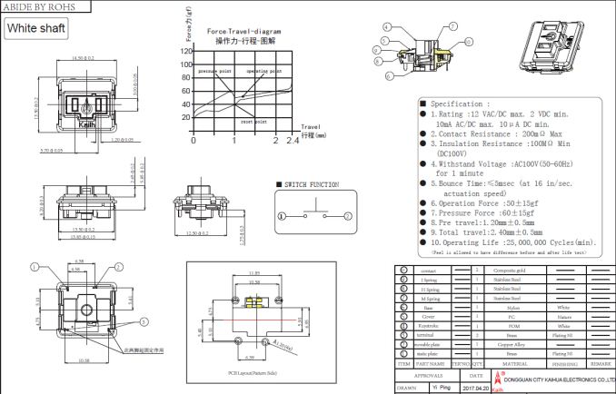
No release date has been announced but we expect to see these on the market on keyboards in coming months.
Related Articles:
- Logitech's G613 "Lightspeed" Wireless Mechanical Keyboard Cuts Wires & Input Lag
- The GSkill KM570 MX Mechanical Keyboard Review: Sturdy and Efficient
- The Kingston HyperX Alloy Elite Mechanical Keyboard Review
More...
-
09-20-17, 06:08 PM #7362
Anandtech: Toshiba To Proceed With Sale Of Memory Business To Consortium For $18B
The latest and possibly final round of bidding for Toshiba's memory business concluded today with Toshiba's board selecting a consortium led by private equity firm Bain Capital as the preferred bidder, over competing bids from Western Digital and Foxconn.
Toshiba has spent most of 2017 trying to sell off their thriving flash memory business in order to offset devastating losses suffered by their Westinghouse nuclear power division. Those financial problems came to a head at the end of 2016 with Toshiba admitting that the losses could amount to several billion dollars, resulting in their stock price falling by more than 40% over a four day span and their bond ratings being downgraded by Moody's and S&P. As the magnitude of their problems became clearer, Toshiba first planned to spin off their memory business and sell a 20% stake, then revised that to selling a majority stake, and eventually settled on selling it outright. As the second largest manufacturer of NAND flash memory, Toshiba's memory business is valued at around $18 billion.
In June, Toshiba selected as preferred buyer a consortium including Bain Capital, Innovation Network Corporation of Japan, Development Bank of Japan and competing memory manufacturer SK Hynix. Toshiba's attempts to sell off the memory business have been complicated by their long-running joint ventures with SanDisk, owned by Western Digital since May 2016. Western Digital and SanDisk have objected to Toshiba's attempts to unilaterally spin off and sell Toshiba's share of the partnerships, with the conflict escalating to arbitration proceedings and lawsuits in both Japan and California. Western Digital has sought all along to acquire the assets Toshiba is putting up for sale, but as the bidding process grew to encompass the entirety of Toshiba Memory and the price climbed, Western Digital had to partner with other investors to continue offering a competitive bid. The uncertainty caused by Western Digital's legal action has been a concern for other bidders, delaying Toshiba's efforts to finalize a deal.
In August, Toshiba re-opened negotiations with Western Digital and their partners, as well as with Foxconn. In the meantime, the Bain-led consortium's offer grew to include investment from Apple, Dell, Kingston and Seagate. Last week, Toshiba announced they had signed a memorandum of understanding with Bain Capital, intending to finalize a deal by the end of September, but not ending negotiations with competing bidders. As recently as September 19, leaks suggested that Toshiba was leaning back toward selling to Western Digital. At a Toshiba board meeting earlier today, Toshiba reaffirmed their commitment to complete a deal with the Bain Capital consortium. The exact sale price has not been made public, nor has the breakdown of the contributions of the individual consortium member companies.
Bloomberg is reporting that Toshiba is prepared to complete this deal even before resolving the legal disputes with Western Digital, by excluding the joint venture assets at issue from the sale and amending the purchase price to compensate. The joint ventures account for less than 5% of the Toshiba memory business, according to Bloomberg's anonymous source.
Toshiba has not yet issued an official statement on today's decision. Western Digital issued a statement expressing disappointment with Toshiba's decision and declaring their intention to continue their legal efforts.
More...
-
09-21-17, 02:32 AM #7363
Anandtech: Imagination Joins the AI Party, Announces PowerVR Series 2NX Neural Networ
In conjunction with today’s PowerVR Series 9XE and Series 9XM announcement, Imagination is revealing a new series of PowerVR-branded hardware IP blocks: the Series 2NX neural network accelerator (NNA). Filling in under the ‘PowerVR Vision and AI’ category as opposed to graphics, the 2NX NNA offers SoC designers dedicated low power hardware for neural network computation and inferencing. While there are many practical applications of such neural networks, Imagination identified mobile devices and smart cameras/surveillance as key markets for the 2NX, as well as automotive and set-top boxes.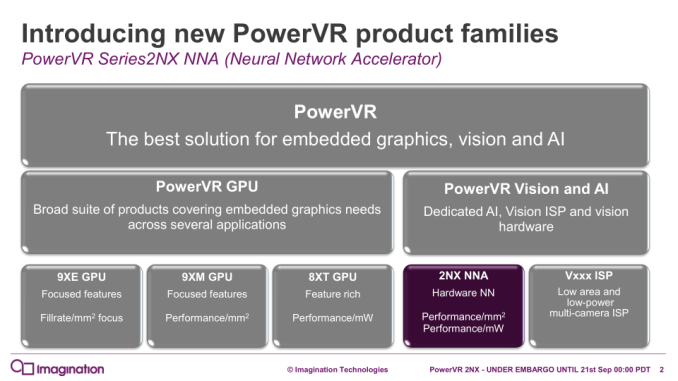
Imagination’s latest IP announcement comes at a time when the market for AI/neural network processing is booming. As what’s arguably the first new processor technology field in several years to take root and reach a rapid growth phase, the industry has been racing to develop neural network processors, establish standards, and otherwise push the boundaries of hardware and software to see just what neural network processing truly can and can’t do. Neural network processing is still in its early, wild west days, but this is the point where companies can attempt to stake their claim in a growing market and, as time goes by, try to be a market leader once the technology matures.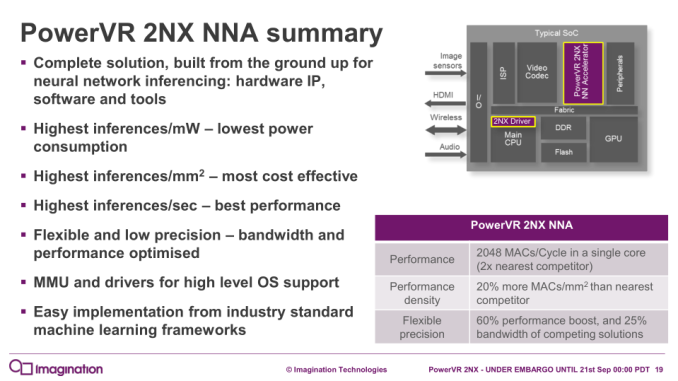
With the announcement of Series 2NX, Imagination is joining Intel, NVIDIA, Apple, Huawei, and other vendors in scoping out the early days of the field. For Imagination this is a natural extension of their existing PowerVR GPU technologies, as current neural network processing is at a very high level a far more restricted form of GPU compute. So this is a field that Imagination can relatively easily get into, and leverage much of their current strengths. At the same time however, for the struggling company this is a badly needed growth market, one that could help the company turn its fortunes. To some degree there’s also a need to keep up with their peers – Imagination would likely be short-sighted not to pursue this – but success here would certainly be a game-changer for the company. The risk, of course, is that the market is still young, and while everyone is eager to get into it, hardware and software vendors alike haven't fully nailed down what tasks can and can't be efficiently handled by a neural network. Being the "hot" thing in tech, right now it's tempting to solve every problem with neural networking, an overzealousness that will abate as the market matures.
Moving on to the technology itself, with the 2NX, Imagination claims the industry’s highest inferencing performance, as well as performance in terms of power consumption (inferences/mW) and area (inferences/mm2). Size-wise, Imagination sees their 2NX solution as going well with a 9XE/9XM GPU, saying that the combined area of a 9XE GPU and 2NX NNA is similar to the total size of a competing mobile GPU. For that mobile market, Imagination plans Android support for the 2NX, and cites the importance of the 2NX’s optional memory management unit (MMU) for Android and other more complex OS’s. In the context of those features, Imagination did explain that they designed the 2NX with mobile designs in mind.
Architecture-wise, like the PowerVR graphics, the 2NX offers a variety of options as it is meant to be licensed out and used in a range of customer-specific use cases. To that end, Imagination describes a single 2NX core as capable of handling 128 to 1024 16-bit and 256 to 2048 8-bit multiply-and-accumulate operations (MACs) per clock, with multiple cores permitting scaling beyond 2048 8-bit MACs/clock.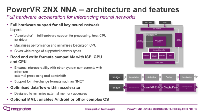
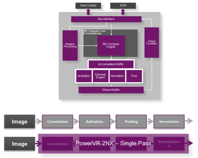
The 2NX accelerator also possesses flexible bit-depth for data and weights, with 16, 12, 10, 8, 7, 6, 5, and 4-bit support, and can be mixed on different layers. In terms of the higher precision 16-bit support, Imagination cites areas like automotive applications, where 16-bit support is mandated. The 2NX also has full variable precision on the internal data formats, with “FP32 precision where required, inside the accumulator with variable output precision.” In turn, the variable weights and precisions can be used to save power and bandwidth as the situation warrants.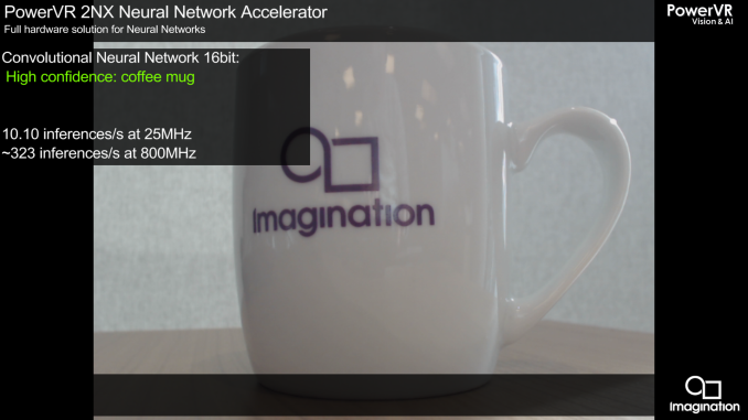
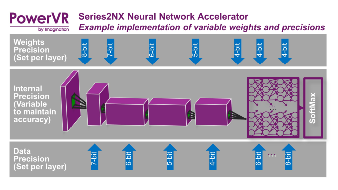
With a specialized driver for the host CPU, the 2NX does all the neural network processing in dedicated hardware blocks, and supports read/write formats compatible with other system blocks like ISPs, GPUs, and CPUs. The 2NX also supports neural network interchange formats, such as Khronos’ NNEF. Imagination has also taken steps to reduce usage of external memory, and offers the aforementioned MMU for the 2NX, especially in light of Android support.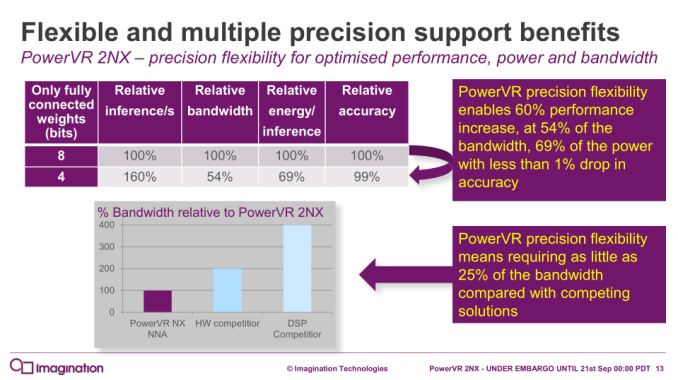
In terms of use cases, like other low-power inferencing processors that have been pitched in the last couple of years, Imagination’s focus is inferencing at the edge. This means automotive, security cameras, smartphones, and other devices that either are their own sensors or close to said sensors, and where there either isn’t the time or connectivity to send all data back to a central host. It’s also at the edge where some of the greatest potential gains from neural network inferencing can be found, as when it’s used correctly, neural network processing can achieve similar results with a fraction of the power consumption of a GPU or DSP (never mind a CPU).
On the software-side, Imagination is releasing their Deep Neural Network (DNN) API, applicable to CPUs, GPUs, and its new NNA. This has the advantage of allowing development and prototyping for the 2NX without having the 2NX on hand, as well as when dealing with multiple SoC configurations.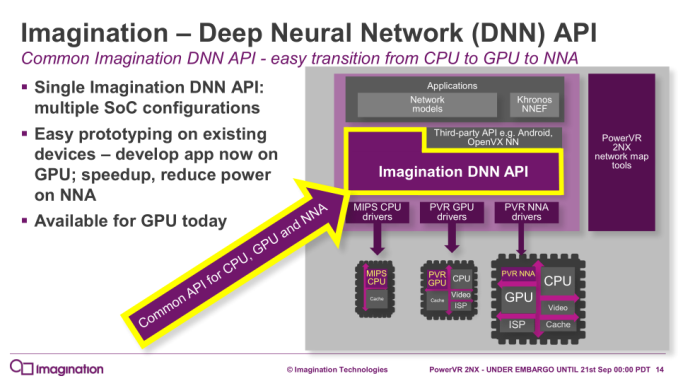
In translating the neural network models to the 2NX itself, Imagination is also providing tuning and evaluation tools, including the PowerVR NX Mapping Tool. As an optional step, from the typically FP32 models trained with frameworks such as TensorFlow and Caffe, PowerVR’s own framework can retrain that model for certain precisions and weights, and thus optimize for the 2NX.
Like the rest of the PowerVR family processors, the 2NX is essentially an IP core that is licensed out to SoC designers. For the mobile sphere, this PowerVR 2NX announcement brings to mind recent announcements of implemented neural network processors inside Huawei’s Kirin 970 and Apple’s A11 Bionic. Earlier, Huawei revealed that the Kirin 970 NPU was accessible by Android Neural Network API support, and in the context of the 2NX for Android, Imagination referred to that API as well, but details are light at this time. For the time being, the 2NX cannot be directly compared to those dedicated inferencing hardware, but will be an interesting topic to revisit as 2NX-equipped products roll out.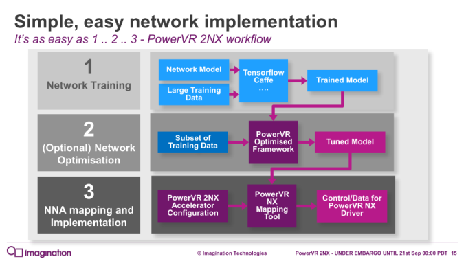
The PowerVR 2NX NNA is available now for licensing, and interested parties may contact Imagination directly.
More...
-
09-21-17, 06:35 AM #7364
Anandtech: GlobalFoundries Adds 12LP Process for Mainstream and Automotive Chips; AMD
GlobalFoundries on Wednesday announced its new 12LP (leading performance) fabrication process. The new manufacturing technology was designed to increase transistor density and improve frequency potential compared to GlobalFoundries’ current-gen 14LPP tech. The company expects the new process to be used by suppliers of various ICs (integrated circuits), including designers of CPUs and GPUs as well as developers of chips for automotive applications and telecommunication solutions. One of the first customers to adopt the 12LP fabrication process will be AMD.
GlobalFoundries’ 12LP manufacturing technology builds upon the company’s 14LPP process that has been used for high-volume manufacturing (HVM) since early 2016. Just like its direct predecessor, the 12LP relies on deep ultraviolet (DUV) lithography with argon fluoride (ArF) excimer lasers operating on a 193 nm wavelength. GlobalFoundries promises that its 12LP provides a 15% higher transistor density and enables a 10% higher frequency potential (at the same power and complexity) compared to “16/14nm FinFET solutions on the market today”. The company does not elaborate which process it used for comparison, but a naturally guess would be its own 14LPP which the company knows well.
The new 12LP relies on the groundwork set by the 14LPP, but uses 7.5T libraries, which is one of the ways that enables GlobalFoundries to shrink die sizes by increasing transistor density. Since the library contains different elements, IC developers have to “recompile” their designs to take advantage of the process. Meanwhile, since the 12LP and the 14LPP are very similar, for GlobalFoundries’ existing customers migration path to the 12LP is pretty straightforward. As for others, they are more likely to use the upcoming 7 nm anyway given the fact that it is not far away.Advertised PPA Improvements of New Process Technologies
Data announced by companies during conference calls, press briefings and in press releasesGlobalFoundries 12LP
vs 14LPP14HP
vs 14LPP7nm Gen 1
vs 14LPPPower - ? >60% Performance 10% ? >40% Area Reduction 15% ? >50%
To a large degree, the 12LP is GlobalFoundries’ response to various manufacturing technologies that build upon the 14/16 offerings and optimize performance and transistor density that have been introduced by various contract makers of semiconductors over the past few quarters. Some of those processes are branded as “12 nm” (e.g., TSMC’s CLN12FFC and Samsung’s 11LPP) and other continuing to carry the “14 nm” monikers (e.g., Samsung’s 14LPC and 14LPU). All three leading foundries — GlobalFoundries, Samsung and TSMC — have been using their 14/16nm-branded technologies for years and have accumulated a lot of knowledge and experience, which is why they could roll out optimized versions of the processes and concentrate on performance and/or transistor density. In addition to this, GlobalFoundries is positioning the 12LP for automotive as well as RF/analogue applications, so there are certain enhancements related to reliability and ability to work in extreme conditions. In particular, GlobalFoundries promises to build a test chip that can work at extreme temperatures from -40°C to +105°C for Automotive Grade 2 qualification in Q4 2017. Keeping in mind lifecycles in the automotive industry, expect the 12LP to stay with GlobalFoundries for many years to come.Comparison of 14 nm Branded Process Technologies GlobalFoundries
12LPGlobalFoundries
14HPGlobalFoundries
14LPP ?TSMC
16FFIntel
14nmFin Pitch ? ? ? ? 42 nm Gate Pitch ? ? 78 nm 90 nm 70 nm Min Metal Pitch ? ? 64 nm 64 nm 52 nm Gate Height ? ? less than 480 nm 480 nm 399 nm Metal Layers 13 17 13 unknown unknown Design Library 7.5T 12T 9T 9T unknown
A legitimate question about the 12LP in the context of automotive applications is who will be GF’s primary customer(s) for the process. There are a number of players developing various chips for automotive applications these days, but when it comes to designers of SoCs that need to pack a lot of transistors, run them at high frequency and be Automotive Grade 2, the list shrinks rather dramatically.
“The world is in the midst of an unprecedented transition to an era of connected intelligence,” said GF CEO Sanjay Jha. “This new 12LP technology provides the performance and density improvements necessary to help our customers continue innovating at the system level, as they deliver real-time connectivity and edge processing to everything from high-end graphics and automobiles to industrial applications.”
In the meantime, AMD will be one of the first to adopt the tech and judging by comments made by Mark Papermaster (AMD CTO) and Sunjay Jha, the chip developer will use the 12LP to make both CPUs and GPUs using the tech.
“We are pleased to extend our longstanding relationship with GlobalFoundries as a lead customer for their new 12LP technology,” said Mark Papermaster, CTO and senior vice president of technology and engineering, AMD. “Our deep collaboration with GF has helped AMD bring a set of leadership high-performance products to market in 2017 using 14nm FinFET technology. We are excited to work with GF on its new 12LP process technology as a part of our focus on accelerating our product and technology momentum.”
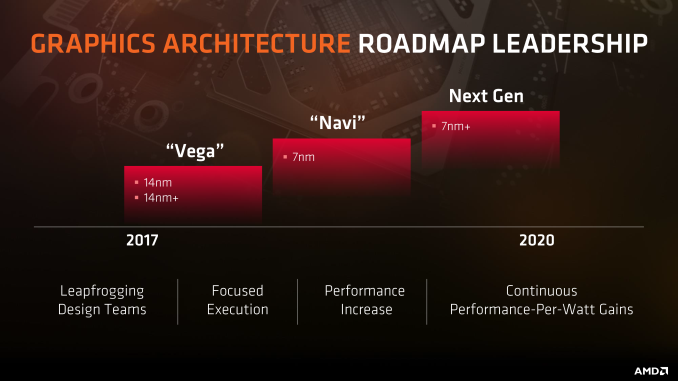
AMD's CPU and GPU roadmaps from earlier this year both listed a "14nm+" node, which at the time was a curious situation since GlobalFoundries didn't have a node between 14nm and 7nm. The obvious takeaway at the time being that GlobalFoundries was developing an interim node - an enhanced version of 14nm - which today's announcement finally confirms. In which case in accordance with Papermaster's official statement, it looks like we should be expecting both Vega and Zen products produced on 12LP in the next year.
To date AMD has said very little about these products. But it's telling that their roadmaps call for existing architectures on the new node rather than their next-generation Navi & Zen 2 architectures, which at least officially, remain scheduled for 7nm. The big question, at least on the GPU side right now, is whether AMD's forthcoming (and still very secretive) Vega 11 GPU is the 12LP product on the company's roadmap, or if AMD is planning on doing a more thorough refresh of Vega at 12LP later on.
Conceptually, all of this is very close to the old "half node" release cadence for GPUs, which would typically see major new GPU architectures released on a new process node, and then smaller and more power-efficient chips released a year later on the interim half node. Half nodes largely died out at 45nm, as fabs opted to put their resources and focus into bringing up whole nodes sooner rather than investing in short-lived half nodes. However as whole node improvements have gone from two year events to three and four year odyssies, it looks like half nodes are back, and with them the refresh chip release strategy.
GlobalFoundries expects to start risk production using the 12LP fabrication technology in Q1 2018. The company does not disclose any timeframes for HVM, but expect them to be different for various chip developers. For example, AMD is a very close partner of GlobalFoundries, so the company gets access to PDKs ahead of many other clients. That said, expect AMD to release its products made using the 12LP rather sooner than later. Mark Papermaster says that the aforementioned chips are to be released in 2018, but he does not elaborate whether to expect them in the first or the second half of the year.
Related Reading:
- Samsung and TSMC Roadmaps: 8 and 6 nm Added, Looking at 22ULP and 12FFC
- GlobalFoundries Details 7 nm Plans: Three Generations, 700 mm², HVM in 2018
- GlobalFoundries to Expand Capacities, Build a Fab in China
- GlobalFoundries Updates Roadmap: 7 nm in 2H 2018, EUV Sooner Than Later?
- AMD Amends GlobalFoundries Wafer Supply Agreement Through 2020, Gaining New Flexibility & New Costs
- EUV Lithography Makes Good Progress, Still Not Ready for Prime Time
More...
-
09-21-17, 08:51 AM #7365
Anandtech: The MSI X299 Gaming Pro Carbon AC Motherboard Review
Intel's HEDT platform in recent times has always had a two CPU generation cadence. The last change was in August 2014, catering for Haswell-E and Broadwell-E, so with the recent launch of Skylake-X, it was time for a refresh: the new LGA 2066 socket and a new X299 chipset, with the inevitable slew of new motherboards looking to capitalize on the margin-rich high-end desktop sector. For our first review, we are testing the X299 Gaming Pro Carbon AC from MSI.
More...
-
09-21-17, 05:11 PM #7366
Anandtech: OWC Launches 13-Port Thunderbolt 3 Dock: GbE, USB-A, SD Card, mDP, FireWir
OWC has launched its new docking solution aimed primarily at Apple’s latest Thunderbolt 3-equipped MacBook Pros. Designed to be the “one dock to rule them all", OWC's Thunderbolt 3 Dock aims to be the most capable TB3 dock on the market, offering a rather sizable selection of both contemporary ports as well as legacy ports that are still be used by various professional applications.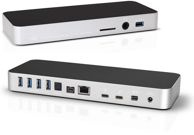
When Apple launched its latest MacBook Pro laptops late last year it received a decent amount of criticism about the notebooks only offering only four Thunderbolt 3 ports for wired connectivity, leaving behind USB Type-A, SD card reader, mDP, and some other things that many people are so used to. At the time, Apple said that docking solutions set to emerge in the future would add ports to the new MBPs and throughout 2017 we have seen a variety of TB3 adapters and docking stations launched. While these products solved mainstream, or, by contrast, specific needs, there were no docking station for the latest-gen MacBook Pro to feature (almost) every popular port that is in use and legacy connectors for those who still need them. The latter are important as Apple has a lot of loyal customers from audio/video industries, some of whom still use have to use FireWire and S/PDIF connectors. OWC’s Thunderbolt 3 Dock, in turn, is adding both contemporary and legacy connectors to the latest MBPs and other laptops with Thunderbolt 3.
In terms of common ports, the OWC Thunderbolt 3 Dock has five USB 3.0 Type-A ports — one on the front and four on the back. Five fully-fledged USB-A connectors is a rare feature for any docking solution, but in a bid to serve certain specific needs, OWC decided to install this number of headers. The OWC TB3 Dock also has an SD card reader, something that would please professional photographers who uses such cards, and for professionals from the audio/video industry an S/PDIF output, a FireWire 800 port, and an additional 3.5-mm audio in/out to connect speakers, mics, and other equipment. While S/PDIF is (still) found on many desktops nowadays, FireWire is becoming increasingly rare. Both are virtually non-existent on contemporary mobile computers, so OWC is addressing a market that is not addressed by PC makers as well as by numerous makers of TB3 adapters/docks.
Moving on to higher bandwidth ports, the dock has both a Gigabit Ethernet and a mDP 1.2 port, both of which are quite popular in both consumer and business environments. Finally, the OWC Thunderbolt 3 Dock has two more full-feature TB3 ports to enable users to connect other TB3 devices. For example, these connectors could be used to plug two 4K displays or a 5K monitor to a non-TouchBar MacBook Pro that has only two TB3 headers one of which will be occupied once the OWC TB3 Dock is plugged in. Obviously, it is simply convenient to keep the display plugged to a dock with all computers and then connect everything from a USB keyboard to speakers to a monitor using just one TB3 cable.
OWC does not disclose how the 13-in-1 dock works, but the complexity of the solution is evidently very high. USB, SD, GbE, FireWire as well as S/PDIF and 3.5-mm in/out audio port require separate controllers. These controllers have to connect to a hub via PCIe bus, underscoring both the flexibility of TB3 and why TB3 devices can also cost so much.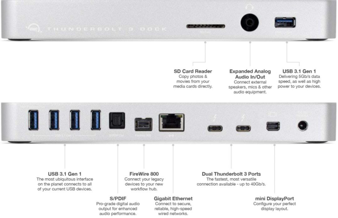
OWC has already started to ship its Thunderbolt 3 Dock, and the product is available directly as well as from retailers like Adorama, B&H Photo and others. The dock is priced at $299, which although still better than some other TB3 docks on the market, is still at the other end of the spectrum comparable to a price of a complete cheap notebook. Though given the number of PCIe-to-X controllers inside, I'm not all that surprised at the price.
Related Reading:
- Apple Announces 4th Generation MacBook Pro Family: Thinner, Lighter, with Thunderbolt 3 & “Touch Bar”
- StarTech's Thunderbolt 3 to Dual 4Kp60 Display Adapters Now Available
- AKiTiO Displays Thunderbolt 3 to 10GBase-T Adapter
- LaCie Announces 2big Dock: 2-Bay TB3 DAS with Card Reader, USB-A and DisplayPort
- HighPoint RocketStor 6618 Thunderbolt 3 DAS: 8-Bays, Up to 96 TB, 2.7 GB/s, $999
- CES 2017: GIGABYTE’s Thunderbolt 3 to 8x USB 3 Dock
- LaCie Launches Rugged and d2 Thunderbolt 3 Storage Devices
- ZOTAC Readies External GPU Enclosure: TB3, 400 W PSU, Due in Q2 2017
- Promise Launches Pegasus3 External Storage via TB3: Up to 48 TB, 1.6 GBps
- LaCie Launches 6big and 12big: Up to 60/120 TB External Storage with Thunderbolt 3
- LaCie Announces Bolt3: 2 TB External SSD at 2.8 GBps over Thunderbolt 3
Gallery: OWC Launches 13-Port Thunderbolt 3 Dock: GbE, USB-A, SD Card, mDP, FireWire & More

More...
-
09-21-17, 06:09 PM #7367
Anandtech: AMD Releases Radeon Software Crimson ReLive Edition 17.9.2: 2-Way Multi-GP
Today, AMD has released Radeon Software Crimson ReLive Edition 17.9.2, bringing 2-way multi-GPU (mGPU) support for RX Vega cards, as well as Project CARS 2 support ahead of tomorrow’s launch. In addition, AMD has included mGPU profile support for Project CARS 2.
Featuring Driver Version 17.30.1091 (Windows Driver Store Version 22.19.677.1), Radeon Software 17.9.2 also fixes two bugs: Hearts of Iron IV system hangs when the campaign scenario is launched, and erroneous “1603 error” messages after successfully installing Radeon Software.
The release of a multi-GPU enabled Vega driver comes at an interesting inflection point for overall multi-GPU support in the industry. NVIDIA's own views are well-known, meanwhile more recently with the Vega launch, AMD has stated that they're also deprioritizing multi-GPU support for Vega and future architectures. The company still supports mGPU - as evidenced by today's driver release - but it's no longer a significant focus as it once was.
The root cause of this dour outlook has been the same on both sides: game engines are increasingly using mGPU-unfriendly rendering technologies, which in turn has made adding mGPU support more difficult for game and driver developers all the while also limiting performance gains. This in turn has created a downward spiral in mGPU usage; as it's no longer a reliable means of getting more performance, the percentage of mGPU system setups has continued to drop, which has further reduced the relevance of the technology. Which is not to write multi-GPU's obituary here and now, only that it's increasingly clear that mGPU is a niche setup and AMD is going to treat it as such.
In any case, in line with AMD's earlier sentiment, Vega's multi-GPU support is only launching with support for up to 2-way configurations, foregoing support for 3+ card configurations. However more interestingly - and perhaps more telling - there is no mention of CrossFire terminology in the press release or driver notes. Rather, the technology is always refered to as "multi-GPU". While the exact mGPU limitations of Vega weren’t detailed, AMD appears to specify that only dual RX Vega56 or dual RX Vega64 configurations are officially supported, where in the past different configurations of the same GPU were officially compatible in CrossFire.
Like all GCN2 and newer cards, RX Vega mGPU is bridgeless and presumably uses the same XDMA technology as introduced in the R9 290X. In selected games, AMD cited performance scaling of over 80%.
The updated drivers for AMD’s desktop, mobile, and integrated GPUs are available through the Radeon Settings tab or online at the AMD driver download page. More information on this update and further issues can be found in the Radeon Software Crimson ReLive Edition 17.9.2 release notes.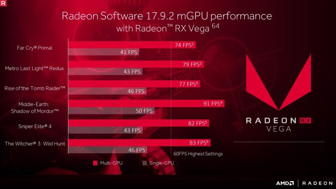
More...
-
09-21-17, 11:40 PM #7368
Anandtech: NVIDIA Releases 385.69 WHQL Game Ready Driver
After last month’s game-heavy 385.41 update, today NVIDIA has followed up by releasing driver version 385.69 with no less than nine Game Ready titles: Project CARS 2 (9/22), Call of Duty: WWII Open Beta (9/29), EVE: Valkyrie – Warzone (9/26), FIFA 18 (9/29), Forza Motorsport 7 (10/3), From Other Suns Open Beta (9/29), Raiders of the Broken Planet (9/22), Star Wars Battlefront II Open Beta (10/6), and Total War: Warhammer II (9/28). This includes Game Ready VR support for EVE and From Other Suns. And as far as bug fixes go, NVIDIA has resolved 14 known issues, making this a rather large update.
Where the original EVE: Valkyrie was only playable with VR headsets (Oculus Rift, HTC Vive, PlayStation VR), EVE: Valkyrie – Warzone is a cross-platform compatible revamp that supports standard desktops with monitors. In turn, this brings the GameWorks graphics technologies found in EVE: Valkyrie to the desktop: volumetric lighting (“God Rays”) and Multi-Sample G-Buffer Anti-Aliasing (MSGAA). Lens Matched Shading has been substituted with Multi-Res Shading, where the resolution on the outer edges of frames is decreased by 30% in order to increase performance.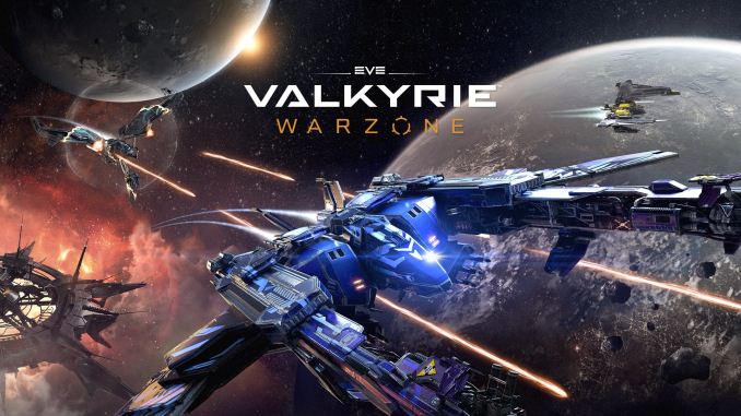
NVIDIA has also brought ShadowPlay Highlights and Ansel support to Raiders of the Broken Planet. First introduced in LawBreakers, the ShadowPlay Highlights functionality now supports a total of four games: LawBreakers, PlayerUnknown’s Battlegrounds, Final Fantasy XV Windows Edition, and Raiders of the Broken Planet.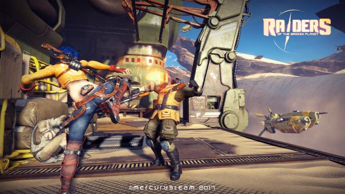
Bug Fixes and SLI Profiles
On the more mundane side of matters, 385.69 brings security updates for driver components. For bug fixes, NVIDIA has resolved the following issues:
- Severe flickering in DOOM after pressing Alt+Tab with SLI enabled and either ShadowPlay instant replay is on or manual capture is in progress.
- The Ctrl+Alt+S keyboard shortcut does not toggle Surround for the GTX 1070
- Low frame rate and lagging in The Binding of Isaac: Rebirth when in full-screen mode on GTX 1050 Ti
- Stuttering when playing games on external display with G-Sync enabled, on notebook GTX 1080s
- HitFilm Express does not respond properly on GTX 970M
- Low frame rates when playing Minecraft in full-screen mode on Optimus notebooks
- Heavy flickering during any OpenGL applications (e.g. Unigine Heaven) on Optimus notebooks
- FPS overlay erroneously appears in Discord if enabled in GeForce Experience
- Low frame rates in Runescape
- Video playback from Windows Store apps stutter and eventually freeze with G-Sync enabled in full-screen mode
- Start menu loads sluggishly when switching focus between a UWP game and Start menu while using Windowed G-Sync
- HDR TV/displays have distorted colors after changing resolution in Windows Control Panel
- NVENC bitrate overshoot occurs at over 240 fps
- Enabled updated .exe for Ansel in Aven Colony
Wrapping things up, NVIDIA has also added or updated the following SLI profiles:
- Dishonored: Death of the Outsider
- Fortnite
- JX3 Online
- Project CARS 2
- Raiders of the Broken Planet
- Total War: Warhammer II
The updated drivers are available through the GeForce Experience Drivers tab or online at the NVIDIA driver download page. More information on this update and further issues can be found in the 385.69 release notes.
More...
-
09-22-17, 07:58 AM #7369
Anandtech: GlobalFoundries Weds FinFET and SOI in 14HP Process Tech for IBM z14 CPUs
GlobalFoundries this week formally introduced its new custom process technology that will be used to manufacture IBM's z14 CPUs, which in turn were announced earlier this year. The 14HP (14 nm, high performance) tech weds FinFET transistors and SOI substrates to get IBM the best of both worlds: small feature sizes and maximized clockspeed potential.
When IBM and GlobalFoundries agreed to transfer semiconductor manufacturing business of the former to the latter, IBM demanded GF to develop and offer custom fabrication processes for IBM’s server CPUs throughout 2014 to 2024 timeframe and involving multiple nodes. Initially the companies talked about custom 22 nm, 14 nm and 10 nm technologies, but in their final announcement they only mentioned a 10-year exclusive supply agreement without disclosing particular nodes. Therefore, it remains to be seen what GlobalFoundries, which is skipping the 10 nm node, is going to offer to its partner (a custom 7 nm is a natural guess). Earlier this year IBM announced its z14 processors for mainframes and this week GlobalFoundries disclosed details about the process technology used to make these chips.
Before we proceed to 14HP, let’s recap what is the IBM z14 and why the blue giant needed a custom technology to build it. The IBM Z mainframes are designed for 24/7/365 availability with zero downtime and are aimed at mission critical applications like credit card processing. IBM Z mainframes are based on specially designed IBM z-series CPUs, which are unique both in terms of microarchitecture, feature set and even physical layout. Each IBM Z14 blade features six CPUs (which IBM calls CPs) carrying processing cores and L2+L3 caches as well as a system control chip (which IBM calls SC) featuring a large L4 cache as well as various interconnects. Each IBM z14 SC CPU consists of 6.1 billion transistors, runs at 5.2 GHz and contains 10 cores with dedicated 6 MB L2 per core (2MB L2 for instructions, 4MB L2 for data) and 128 MB shared L3. Meanwhile, the system control (SC) chip consists of 9.7 billion transistors and features 672 MB of L4 and interconnects to ensure coherency between CPUs. Needless to say, that both CP and SC are extremely complex and benefit from manufacturing technologies with small feature sizes.
Being very complex and very fast, IBM’s CPUs for z-series mainframes were historically produced using custom fabrication processes that were architected to deliver maximum performance, manufacturing costs be damned. In fact, it was IBM whom first used SOI substrates to build its RS64-IV codenamed ‘Istar’ PowerPC-AS CPUs in 2000, which was then followed by AMD and others whom used SOI to build their own highly-successful processors. The use of SOI enables a tangible increase of CPU clock rates without a massive increase of power consumption, but a SOI wafer substrate costs more than a bulk substrate, so this is exactly what GlobalFoundries’14HP is about.
GlobalFoundries says that the 14HP process technology leverages “the proven 14nm FinFET high-volume experience of our Fab 8 facility”, but does not explicitly say that 14HP is based on 14LPP; only that it uses SOI substrates instead of bulk ones. In fact, looking at the numbers it appears to be substantially different. When compared to GF’s 14LPP and similar bulk FinFET process technologies, 14HP can support up to 17 metal layers (vs. 13 for the 14LPP) and uses 12T libraries (vs. 9T and 7.5T for various 14 nodes). As for experience, 14HP will be utilized across the same ASML TWINSCAN NXT scanners that the company uses to produce existing chips using its current FinFET technologies.Comparison of 14 nm Branded Process Technologies GlobalFoundries
12LPGlobalFoundries
14HPGlobalFoundries
14LPP ?TSMC
16FFIntel
14nmFin Pitch ? ? ? ? 42 nm Gate Pitch ? ? 78 nm 90 nm 70 nm Min Metal Pitch ? ? 64 nm 64 nm 52 nm Gate Height ? ? less than 480 nm 480 nm 399 nm Metal Layers 13 17 13 unknown unknown Design Library 7.5T 12T 9T 9T unknown
GlobalFoundries is not disclosing too many specific details about 14HP, which isn't all that surprising given the situation at hand. There is a single customer that is going to use it, and IBM does not want to share too many details about how it designs its processors as well. So, while we do understand that SOI can help with increasing frequencies and voltages compared to bulk process technologies, we do not have precise numbers here.
Related Reading:
- Hot Chips: IBM's Next Generation z14 CPU Mainframe Live Blog (5pm PT, 12am UTC)
- GlobalFoundries and AMD Announce First 14nm FinFET Sample Production Success
- GlobalFoundries Adds 12LP Process for Mainstream and Automotive Chips; AMD Planning 12LP CPUs & GPUs
- GlobalFoundries Details 7 nm Plans: Three Generations, 700 mm², HVM in 2018
- GlobalFoundries to Expand Capacities, Build a Fab in China
- GlobalFoundries Updates Roadmap: 7 nm in 2H 2018, EUV Sooner Than Later?
More...
-
09-22-17, 06:36 PM #7370
Anandtech: GSkill Announces New AMD Compatible Trident Z RGB Kits
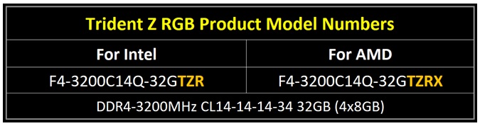
With both AMD Ryzen and Threadripper platforms continuing to mature, we’ve seen an increase in the two platform’s ability to handle higher capacity and faster RAM and be stable. It is more common today to reach 3200MHz than it was upon release due in part to better BIOS from board partners and memory testing. To that end, G.Skill announced a new lineup of Trident Z RGB DDR4 Memory for AMD. The kits said to have enhanced compatibility on the latest AMD platform with faster and higher density kits including RGB LEDs for enhanced visuals.
G.Skill's announcement includes a full range of memory kit capacity options with new kits available starting at DDR4 2400Mhz. They come in two, four, and eight module configurations with 8GB and 16GB modules allowing capacities ranging from 16GB to 128GB. The high-capacity 128GB sets can reach speeds up to 2933MHz CL14 while speeds up to 3200Mhz CL14 are possible up to 32GB (4x8GB) setups. The kits are good for the both the dual-channel Ryzen platform or quad-channel X399 Threadripper platform.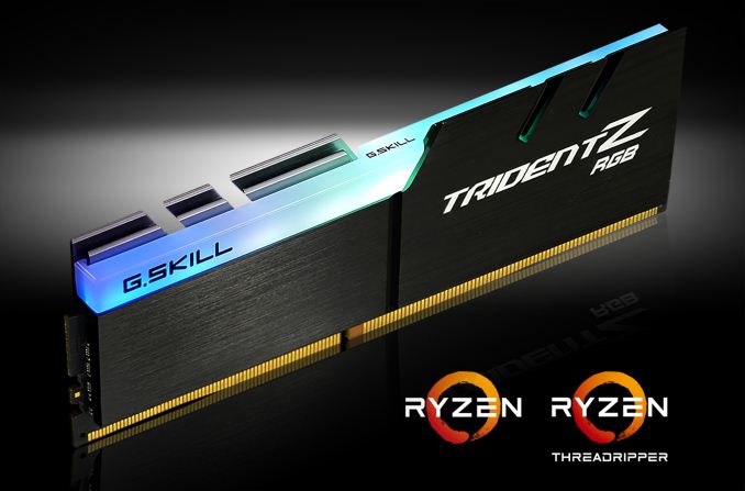
Buyers will be able to discern between the new Trident Z RGB kits from the original as the new product model number will have an “X” at the end. I’ll imagine we will see the Ryzen and Ryzen Threadripper moniker somewhere on the retail packaging as well. The new Trident Z RGB models support OC profile DOCP – Direct Memory Profile, on compatible motherboards. Users should be able to enable DOCP in the BIOS and boot to the Memory’s rated speeds. For the best chance at success, be sure your motherboard has the latest BIOS.
 The full lineup will be available through GSkill distribution partners in October. Pricing was not listed but is expected to be the same or close to its Intel counterparts.
Trident Z RGB Model Compatibility List for AMD Platforms DDR4 Frequency CL Timing Kit Capcity Voltage For Ryzen For Threadripper 3200MHz 14-14-14-34 32GB (4x8GB) 1.35 Y 16GB (2x8GB) Y 2933MHz 14-14-14-34 64GB (8x8GB)
128GB (8x16GB)1.35V Y 16-16-16-36 64GB (8x8GB)128GB (8x16GB)Y 2400MHz 15-15-15-35 64GB (8x8GB)128GB (8x16GB)1.2V Y 32GB (4x8GB)64GB (4x16GB)Y Y 16GB (2x8GB)32GB (2x16GB)Y Y
Related Reading:
- An AMD Threadripper X399 Motherboard Overview: A Quick Look at Seven Products
- AMD Announces Ryzen AGESA 1.0.0.6 Update: Enables Memory Clocks Up To DDR4-4000
- Retesting AMD Ryzen Threadripper's Game Mode: Halving Cores for More Performance
- The AMD Ryzen Threadripper 1950X and 1920X Review: CPUs on Steriods
- The AMD Zen and Ryzen 7 Review: A Deep Dive on 1800X, 1700X, and 1700
- The AMD Ryzen 3 1300X and Ryzen 3 1200 CPU Review: Zen on a Budget
More...


 Quote
QuoteThread Information
Users Browsing this Thread
There are currently 17 users browsing this thread. (0 members and 17 guests)


Bookmarks