

Results 7,431 to 7,440 of 12096
Thread: Anandtech News
-
10-17-17, 11:13 AM #7431
Anandtech: Microsoft Introduces Surface Book 2: 7th/8th Generation i5/i7 CPUS, NVIDIA
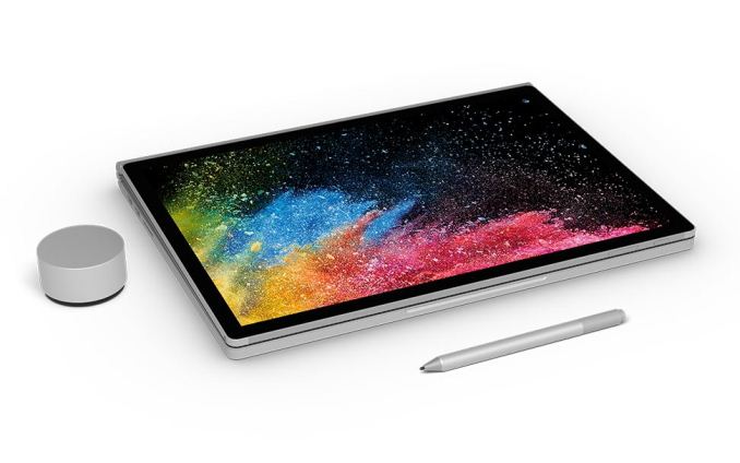
In what some would call a surprise announcement, Microsoft has unveiled the much anticipated Surface Book 2, 2 in 1 laptop. With content creators, designers, and PC gamers requiring more and more horsepower for demanding tasks, the two-year-old Surface book could be perceived as a bit long in the tooth. And while the Surface Book is a solid 2 in 1, people still wanted more out of their device. Microsoft says the Surface Book 2, “removes the barrier between the desktop and the laptop by giving mobile professionals the power of a desktop, the versatility of a tablet, and the freedom of a light and thin laptop…”
The appearance of the SB2 compared to the original looks to be identical with its silver magnesium case and the familiar Muscle Wire hinge making its way forward as well. When closed, due to the special hinge, it looks like a book closed over a pencil as there as a gap towards the hinge side which shrinks to nothing as it nears the opposite end. The keyboard also looks the same and uses LED backlit keys for ease of use in low light situations. Ports on the outside consist of two USB 3.0 (5 Gbps) Type-A, and one USB Type-C. It also has a UHS-II SDXC card reader and for audio a 3.5mm headphone jack.
The Surface Book 2 will come in two main options; either the 13.5”, 3000 x 2000 PixelSense display (found in the original SB), or now in a 15” 3240 x 2160 Pixelsense Display. Both options are 10-point multi-touch capacitive screens and still use a 3:2 ratio instead of the more popular 16:9. The monitor supports the Surface Pen and Surface Dial on-screen support. Microsoft worked with Adobe for increase integration between the Surface Book 2 and Adobe Creative Cloud with new Surface Dial functionality in Photoshop letting users to more easily access and change your most frequent brush settings.
The latest SB2 is now powered by Intel’s 8th Generation Core processors and offer NVIDIA GTX 1050 2GB in the 13.5" model, or GTX 1060 2GB discrete graphics options in the larger 15" version. The graphics upgrades are a significant update from the original which shipped with a GT 940MX, but the new models appear to follow the thermal design of Performance Base version of the Surface Book which shipped with a GTX 965M as a mid-cycle upgrade. If a discrete video card isn’t necessary, the CPUs had Intel HD/UHD Graphics 620 integrated GPUs. With the use of more powerful discrete GPUs, 1080p PC gaming at 60 FPS is possible according to Microsoft. With this, the SB2 is ready for Windows Mixed Reality applications using a compatible headset and controller.
The two CPU options are a 7th Generation i5-7300U with 2C/4T sporting a 2.6 GHz base clock and up to 3.5 GHz Turbo, and the 8th Generation i7 8650U with 4C/8, a base clock of 1.9 GHz and Turbo to 4.2 GHz. Microsoft says the SB2 will provide “all-day” battery life – up to 17 hours of video playback with the i5 version. No mention of how long it will last with more intense use or through testing software but are quick to share it is 70% more than the latest MacBook Pro. Storage options range from a 256GB SSD to a 1TB SSD, while RAM capacity is either 8GB/16GB of LPDDR3-1866.
On the multimedia side of things, there is a 5MP front-facing camera with 1080p HD video and an 8MP rear-facing autofocus camera with 1080p Full HD video. The front-facing camera has IR capabilities since the SB2 works with Microsoft Hello. Audio input put is handled by dual stereo microphones while there are two front-facing speakers with Dolby Audio Premium. Wireless connectivity is integrated and supports 802.11a/b/g/n/ac as well as Bluetooth 4.1 LE. The 15" model has Xbox Wi-Fi Direct built in for gaming with compatible controllers as well.
Pricing starts at $1499 for the smaller model, and $2499 for the new 15" version. The Surface Book 2 13" will be available for pre-order starting November 9th in the US and other markets around the world along with the Surface Book 2 15" in the US at the Microsoft Store and Microsoft.com. Delivery begins on November 16th.
Related Reading:Microsoft Surface Book 2 Warranty Period 1 Year Limited Hardware Product Page Microsoft Surface Book 2 Price N/A Type 2 in 1 Processor Family 7th and 8th Generation Intel Core i5 and i7 Processors i7-7300U 2C/4T (2.6 GHz base, 3.5 GHz Turbo)
i7-8650U 4C/8T (1.9 GHz base, 4.2 GHz Turbo)Maximum Memory SODIMM
8GB/16GB
Dual Channel
LPDDR3-1866Network Connectivity 802.11 a/b/g/n/ac
Bluetooth 4.1 LEInternal Storage 256GB, 512GB, or 1TB SSD Available Graphics Integrated: Intel HD 620 or UHD 620
Discrete: NVIDIA GTX1050 (13.5") or GTX 1060 (15")Expansion Slots 1 x UHS-II SDXC Card Reader Display 13.5", 3000 x 2000 resolution PixelSense Display
15" 3240x 2160 resolution, PixelSense Display
Both 10-point multi-touch G5Ports and Connectors 2 x USB3.0 (5 Gbps) Type-A
1 x USB Type-C
3.5" headphone jack
2 Surface ConnectInput Device Backlit keyboard with function key control
Optional Surface Pen
Optional Surface DialCamera 5MP front-facing camera with 1080p HD video
8MP front-facing camera with 1080p Full HD vido
Dual Microphones
Front-facing stereo speakers with Dolby Audio PremiumPower Details not listed Dimensions
(W x D x H)13.5" (i5) 12.3" x 9.14" x 0.51-0.90"
13.5" (i5) 12.3" x 9.14" x 0.59-0.90"
15" (i7) 13.5" x 9.87" x 0.59-0.90"Weight 13.5" Starting at 3.38 lbs including keyboard
15" Starting at 4.2 lbs including keyboard
- Best Laptops: Q3 2017
- Clevo Announces P870TM Laptop: First DTR Laptop with Coffee Lake-S
- HP Announces Omen X Laptop: 17.3" LCD, Core i7 + GeForce GTX with Overclocking
More...
-
10-18-17, 02:35 AM #7432
Anandtech: NVIDIA Brings Back Destiny 2 Bundle Again for GTX 1080 & 1080 Ti Cards
For what is the 3rd time this year, NVIDIA is offering the “New Legends Will Rise” Destiny 2 bundle for GeForce GTX 1080 and 1080 Ti graphics cards, systems, and laptops. From today until November 29th (or while supplies last), qualified purchases will come with a digital copy of Destiny 2 via Blizzard Desktop App, officially launching on October 24th for PC. As a reminder, eligible systems may include NVIDIA’s own GeForce GTX Battlebox PCs.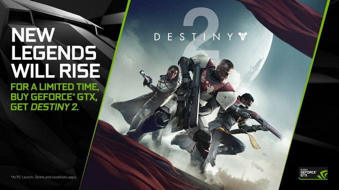
The massively multiplayer online sci-fi first-person shooter, a concept Bungie previously described as a “shared world shooter”, supports High Dynamic Range (HDR) and SLI. Having collaborated with Activision and Bungie on the game's graphics, NVIDIA has detailed the PC graphics options for Destiny 2 in a blog post, with the removal of MSAA the only difference from the Beta. In addition, GTX 1060 performance testing at 1080p was done for each graphical option. At a glance, Destiny 2 seems to be considered as a genuine improvement over the original, not to mention the PC availability.
The game codes may only be redeemed until December 31st. Fortunately, this comes just after at the end of the Middle-earth: Shadow of War bundle for GTX 1080 and 1080 Ti cards. Otherwise, no other bundles are active this time.
On the bundle page, NVIDIA has listed an Amazon link for a list of qualifying cards.NVIDIA Current Game Bundles
(10/18/17)Video Card
(incl. systems and laptops)Bundle GeForce GTX 1080Ti/1080 Destiny 2 Bundle GeForce GTX 1070 None GeForce GTX 1060/1050Ti/1050 None
Buy EVGA GTX 1080 Ti SC BE G on Amazon.com
Buy ASUS GTX 1080 ROG STRIX on Amazon.com
The bundle landing page has links to all eligible retailers. Codes must be redeemed through GeForce Experience (3.2.2 or higher), utilizing driver 373.06 or higher. Game must be redeemed via GeForce Experience on a desktop or notebook PC with the qualifying graphics card installed. Once the code is redeemed in GeForce Experience, the game must be redeemed in the Blizzard Desktop App in seven days. A Blizzard account is required to redeem and play the game. Be sure to verify the participation of any vendors purchased from as NVIDIA will not give codes for purchases made from non-participating sellers.
More...
-
10-18-17, 07:37 AM #7433
Anandtech: Intel Shipping Nervana Neural Network Processor First Silicon Before Year
This week at the Wall Street Journal’s D.Live 2017, Intel unveiled their Nervana Neural Network Processor (NNP), formerly known as Lake Crest, and announced plans to ship first silicon before the end of 2017. As a high-performance ASIC custom-designed and optimized for deep learning workloads, the NNP is the first generation of a new Intel product family, oriented for neural network training. From the beginning, the NNP and its Nervana Engine predecessor have aimed at displacing GPUs in the machine learning and AI space, where applications can range from weather prediction and autonomous vehicles to targeted advertising on social media.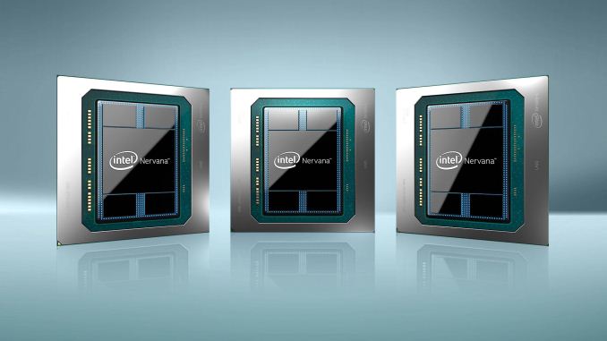
Under development for the past three and a half years, the NNP originated as the Nervana Engine deep learning ASIC, which was announced in May 2016 and had all the marquee features of the NNP: HBM2, FlexPoint, cacheless software memory management, and a high-speed interconnect. Not too long after, Nervana was acquired by Intel in August 2016. Later that November during Intel’s AI Day, the Nervana Engine rematerialized to the public as Lake Crest, with first silicon due in 1H 2017. In that sense, the product has been delayed, although Intel noted that preliminary silicon exists today. Nevertheless, Intel commented that the NNP will be initially delivered to select customers, of which Facebook is one. In fact Intel has outright stated that they collaborated with Facebook in developing the NNP.
In terms of the bigger picture, while the past year has seen many announcements on neural network hardware accelerators, it is important to note that these processors and devices operate at different performance levels with different workloads and scenarios, and consequently machine learning performance consists of more than a single operation or metric. Accelerators may be on the sensor module or device itself (also known as on the ‘edge’) or farther away in the datacenters and the ‘cloud.’ Certain hardware may be training deep neural network models, a computationally intensive task, and/or running inference, applying these trained network models and putting them into practice. For Intel's NNP today, the coprocessor is aimed at the datacenter training market, competing with solutions like NVIDIA’s high-performance Volta-based Tesla products.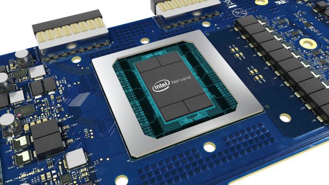
This segmentation can be seen in Intel’s own AI product stack, which includes Movidius hardware for computer vision and Altera for FPGAs, as well as Mobileye for automotive. The offerings are bisected again with the datacenter, which formally encompasses Xeon, Xeon Phi, Arria FPGAs, and now the NNP. For the NNP family, although the product announced today is a discrete accelerator, the in-development successor Knights Crest will be a bootable Xeon processor with integrated Nervana technology. While Intel referred to an internal NNP product roadmap and mentioned multiple NNP generations in the pipeline, it is not clear whether the next-generation NNP will be based on Knights Crest or an enhanced Lake Crest.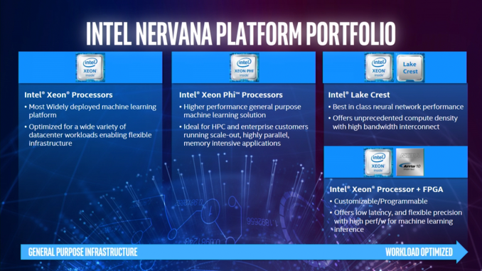
On the technical side of matters, the details remain the same from previous reports. Intel states that the NNP does not have a "standard cache hierarchy," however it does still have on-chip memory for performance reasons (I expect serving as registers and the like). Managing that memory is done by software, taking advantage of deep learning workloads where operations and memory accesses are mostly known before execution. Subsequently, the lack of cache controllers and coherency logic frees up die space. Otherwise for off-die memory, the processor has 32GB of HBM2 (4 8-Hi 1GB stacks) on the shared interposer, resulting in 8 terabits/s of access bandwidth.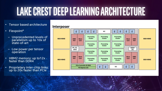
Bringing to mind Google's TPU and NVIDIA's Tensor Cores, the NNP's tensor-based architecture is another example of how optimizations for deep learning workloads are reflected in the silicon. The NNP also utilizes Nervana’s numerical format called FlexPoint, described as in-between floating point and fixed point precision. Essentially, a shared exponent is used for blocks of data so that scalar computations can be implemented as fixed-point multiplications and additions. In turn, this allows the multiply-accumulate circuits to be shrunk and the design made denser, increasing the NNP’s parallelism while reducing power. And according to Intel, the cost of lower precision is mitigated by the inherent noise in inferencing.
The focus on parallelism continues with the NNP’s proprietary high-bandwidth low-latency chip-to-chip interconnect in the form of 12 bi-directional links. Additionally, the interconnect uses a fabric on the chip that includes the links, such that inter-ASIC and intra-ASIC communications are functionally identical "from a programming perspective." This permits the NNP to support true model parallelism as compute can be effectively distributed, taking advantage of the parallel nature of deep neural networks. Additional processors can combine to act as a single virtual processor with near linear speedup, where, for example, 8 ASICs could be combined in a torus configuration as shown above.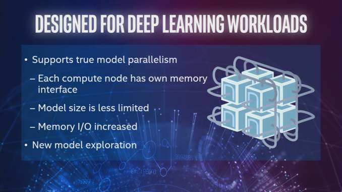
Presumably, the NNP will be fabricated on the TSMC 28nm process that Lake Crest was intended for; just after the acquisition, the Nervana CEO noted that production of the 28nm TSMC processors was still planned for Q1 2017. In any case, 16nm was explicitly mentioned as a future path when the Nervana Engine was first announced, and the CEO had also expressed interest in not only Intel’s 14nm processes, but also its 3D XPoint technology.
More...
-
10-18-17, 07:37 AM #7434
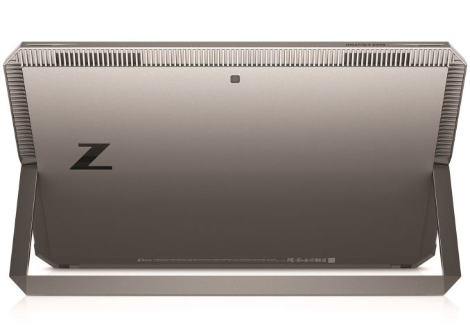
Anandtech: HP Announces ZBook x2: HP's First Detachable Workstation
Today at the Adobe MAX conference in Las Vegas, HP will showcase their new HP ZBook x2. The ZBook x2 will be HP's first detachable PC workstation, and, HP claims, the most powerful. The new ZBook x2 is the latest of several detachable PC releases from HP that started earlier this year. The HP Spectre x2 and HP Elite were introduced earlier with an updated appearance and hardware specifications. HP’s goal with the ZBook x2 was to maintain creative workflows for artists, designers, and digital imaging professionals, and increase productivity without leaving their creative flow to do so.
For their latest worktation-class product, HP worked with customers from amateurs to professionals in determining workflow bottlenecks and how to get around them. What they found was an age-old complaint: devices were not delivering the performance users wanted, and lag plus instability further hurt usability. Their blueprint to fix these problems is to have a better application experience, better visualizations, and higher reliability for increased productivity.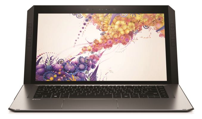
HP took the ZBook x2 and, working closely with Adobe, optimized it for Adobe's CC apps. It has four modes, Table Mode (Capture), Detach mode (create), dock mode (produce), and Laptop mode (review) allowing for a lot of versatility using its integrated stand, detachable keyboard, pen, and touch-enabled display. The display is a 14” 4K UHD Dreamcolor unit; a 10 bit display (8 bit + FRC) supporting 1 billion colors and 100% Adobe RGB with factory calibration.
It is pen and touch-enabled and comes with an anti-glare coating to minimize reflections in bright ambient light. On both sides of the display are 18 quick keys; these quick keys offer 3 preset shortcuts for Adobe Photoshop, Illustrator, and Lightroom. When working in tablet mode, users have access to their shortcuts without a keyboard using these keys (programmable as well) which keeps efficiency intact. The pen itself uses a passive, battery-less technology (Wacom EMR)- never needs charging, claims to have virtually zero latency, and has a total of 4,096 pressure sensitive levels. Unfortunately, the pen does not come with the device and is sold separately.
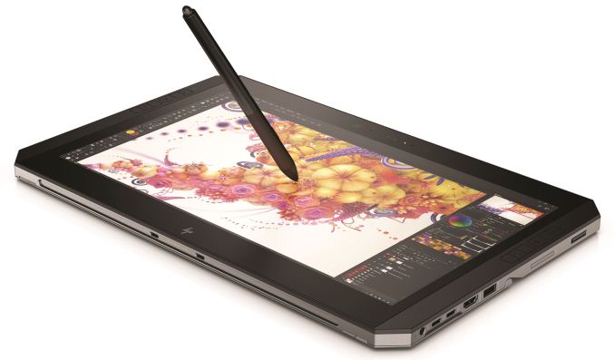
The aluminum decked backlit LED keyboard, HP says, is a full-size commercial keyboard made mobile. The keys sport 1.5mm travel and 18.7mm pitch and is detachable for additional freedom of use. Connectivity between the system and keyboard is via Bluetooth when not connected. The monitor also has three webcams: two front-facing 720p, one with IR capabilities, and an 8MP world facing camera. With the front IR camera, the device is capable of supporting Microsoft Hello.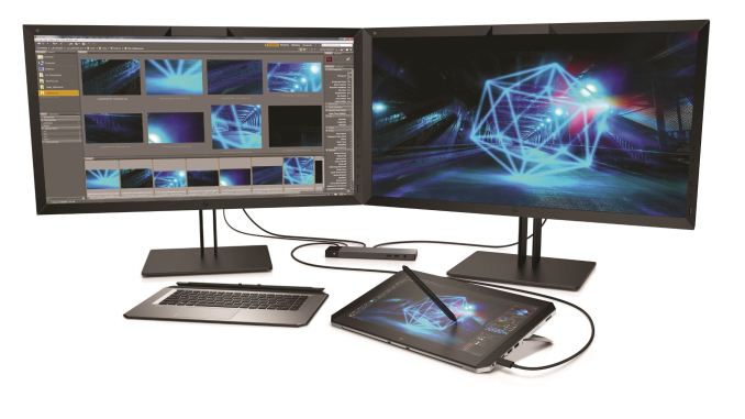
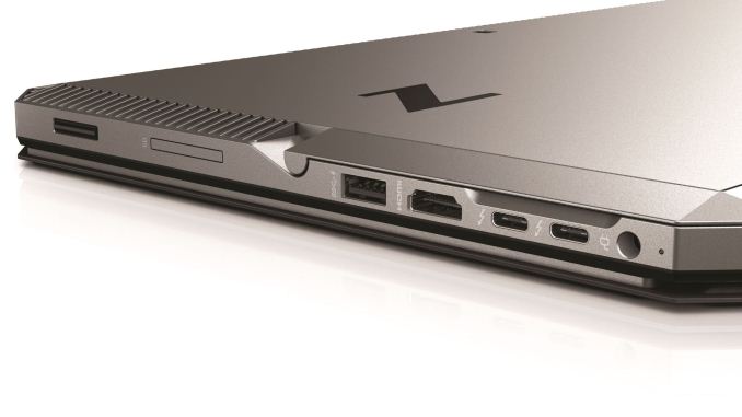
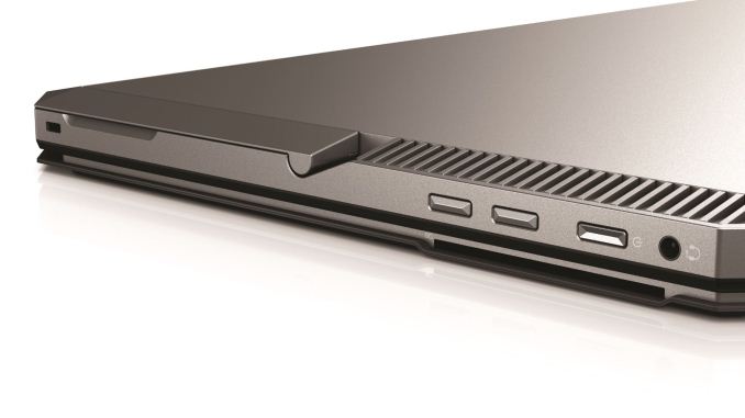
Internally, the ZBook x2 supports both 7th and 8th generation Intel CPUs from the i7-7500U to the i7-8650U. The flagship CPU, i7-8560U, comes in with a base clock of 1.9 GHz and boosts up to 4.2 GHz. Memory capacity is up to 32GB DDR4-2133 non-ECC SDRAM across 2 SODIMMs. 32GB of ram is double what most other detachables provide helping with multitasking and large file manipulation. Internal storage options range from a 128GB M.2 SATA SSD, up to 2TB PCIe NVMe M.2 SSD. Internal storage is not user upgradeable, however, there are two Thunderbolt 3 ports for additional external connectivity as well as a USB 3.0 Type-A port, which HP lists as having "charging" capabilities.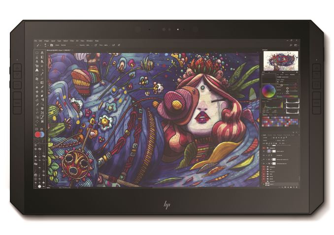
Available graphics include the Intel HD 620 or UHD 620 built into the devices CPUs, or a discrete GPU as an option in the NVIDIA Quadro M620 (2GB GDDR5 dedicated). Networking capabilities are all wireless and handled by the HP HS3110 HSPA + Intel Mobile broadband module. It is dual-band wireless AC and supports Bluetooth 4.2. In order to keep these devices cool, HP reinvented their cooling solution for the ZBook x2. Dual fans take in cooler air from the sides, run it across the hot spots through heat pipes, and exhaust it out of the top. The 70 Wh Li-ion battery is said to last up to 10 hours with Hybrid graphics and Intel HD graphics configurations.
HP says pricing isn’t available for global markets yet, however, the starting price for the US is $1749. They will begin shipping in early December.
Related Reading:HP ZBook x2 Warranty Period 3 Year or 1 Year options available Product Page N/A Price Starting at $1749 (US) Type 2 in 1 detachable Processor Family 7th and 8th Generation Intel Core i5 and i7 Processors i7-7500U (2.7 GHz base, 3.5 GHz Turbo)
i7-7600U (2.8 GHz base, 3.9 GHz Turbo)
i5-8250U (1.6 GHz base, 3.4 GHz Turbo)
i7-8550U (1.8 GHz base, 4 GHz Turbo)
i7-8650U (1.9 GHz base, 4.2 GHz Turbo)Maximum Memory Two SODIMM
32GB
Dual Channel
DDR4-2133 non-ECC SDRAMNetwork Connectivity Dual Band Wireless AC 8265
802.11 a/b/g/n/ac (2x2)
Bluetooth 4.2Internal Storage 128 GB M.2 SATA SSD
512 GB M.2 SATA FIPS SSD
256 GB - 512GB HP Z Turbo Drive (PCIe NVMe)
256 GB - 2TB PCIe NVMe M.2 SSD
512 GB PCIe NVMe SED SSDAvailable Graphics Inegrated: Intel HD 620 or UHD 620
Discrete: NVIDIA Quadro M620 (2 GB dedicated GDDR5)Expansion Slots 1 x Smart card reader
1 x Media card readerDisplay 14" 4k IPS anti-glare
14" 4K Dreamcolor anti-glare touchscreenPorts and Connectors Left side:
1 x headphone/microphone combo
Right side:
1 x Power Connector
1 x HDMI 1.4
1 x USB 3.0 Type-A (charging)
2 x USB 3.1 Type-C Thunderbolt 3 (DisplayPort 1.2)Input Device Backlit keyboard with function key control
Image sensor clickpad with on/off button, two-way scroll, gestures, two buttons
Extra large clickpad with on/off button, two-way scroll, gestures, two buttonsCamera 720p HD webcam with IR (front-facing)
720p HD webcam (front-facing)
8 MP Camera (world facing)Power 90W External AC Power adapter
65W External AC Power adapter
4-cell 70Wh Li-ion polymer Up to 10 hoursDimensions
(W x D x H)14.25" x 8.94" x .8" (Laptop Mode)
14.35" x 8.94" x .57 (Tablet Mode)Weight Starting at 4.78 lbs (Laptop Mode)
Starting at 3.64 lbs (Tablet Mode)- Microsoft Introduces Surface Book 2: 7th/8th Gen i5/i7 and NVIDIA Discrete Graphics
- Best Laptops: Q3 2017
- Clevo Announces P870TM Laptop: First DTR Laptop with Coffee Lake-S
- HP Announces Omen X Laptop: 17.3" LCD, Core i7 + GeForce GTX with Overclocking
Gallery: HP ZBook X2 Gallery


More...
-
10-18-17, 09:31 AM #7435
Anandtech: G.Skill Launches Lineup of Trident Z Kits for Coffee Lake: DDR4 at 3733 -
G.Skill has launched a new series of memory module kits optimized for Intel’s new 8th Generation Core processors. The new DIMMs belong to G.Skill’s Trident Z and Trident Z RGB families and are guaranteed to operate at 3733 – 4600 MT/s data transfer rates when paired with Intel's Coffee Lake processors. Some of the modules need significantly increased voltages and thus require higher-end motherboards that can deliver “clean” power.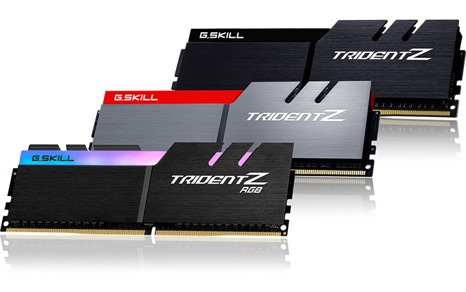
Getting right down to business, the fact that G.Skill even announced memory kits specifically for Coffee Lake got an eyebrow raise out of us. At first blush, it seemed like a marketing stunt, especially since they're using the same Samsung’s B-die chips that they've been using for some time now. But according to the company, Coffee Lake's memory controller behaves ever so slightly differently than Kaby Lake's when overclocked, necessitating the new modules.
Sure enough then, if we compare G.Skill's DDR4-4200 and DDR-4600 modules for the new Coffee Lake/Z370 and the Kaby Lake-X/X299 platforms, we will notice that the modules for Coffee Lake have looser tRAS sub-timings than the modules for Kaby Lake. From performance point of view, tRAS might not be a big deal, but it's an unexpected change; if anything we would have expected Coffee Lake to accept the same timings as Kaby Lake. There are a few possible reasons for this difference - not the least of which is the immature Z370 platform - however the more interesting options are that it's a product of the new manufacturing process, or possibly even a new memory controller entirely (especially seeing as how Coffee Lake doesn't support DDR3).
Otherwise, G.Skill's tinkering only seems to have been necessary for their fastest modules, as their lower-clocked enthusiast-class memory sticks are unchanged from earlier revisions. Conversely, since G.Skill has just loosened the timings of their new high-speed DIMMs, they should continue to work fine in other platforms.
Overall, G.Skill’s lineup of Coffee Lake-optimized DRAM kits consists of seven products featuring two or four 8 GB or 16 GB modules based on Samsung’s B-die chips. The rather broad family of Coffee Lake-optimized memory products is aimed at different classes of systems. The fastest DDR4-4400/4500/4600 DIMMs are only available in 8GB capacities and require 1.4 V, 1.45 V or even 1.5 V. G.Skill positions these modules for enthusiasts seeking maximum performance and not interested in maximizing DRAM content per box. G.Skill’s ‘mid-range’ kits for Coffee Lake run at DDR4-4000/4200, have 32 GB of capacity (16 GB DIMMs), and are designed for those who need high memory bandwidth along with a decent amount of RAM. Finally, there is a 64 GB DDR4-3733 kit for users who run memory-intensive applications.Evolution of Intel DDR4 Memory Controllers for Socketed CPUs Haswell-E Skylake Broadwell-E Kaby Lake Skylake-X Coffee Lake Supported Standards DDR4-2133 DDDR4-2133
DDR3L-1600DDR4-2400 DDR4-2400
DDR3L-1600DDR4-2666 DDR4-2666 Number of Channels 4 2 4 2 4 2 DIMMs per Channel 2 Voltages 1.2 V 1.2 V
1.35 V1.2 V 1.2 V
1.35 V1.2 V 1.2 V Launch Timeframe Q3 2014 Q3 2015 Q2 2016 Q1 2017 Q2 2017 Q4 2017
Traditionally, all the Trident Z modules come with XMP 2.0 SPD profiles to simplify their setup on optimized platforms. In addition, the modules are equipped with G.Skill’s proprietary aluminum heat spreaders. Meanwhile, the Coffee Lake-optimized lineup from G.Skill also includes two Trident Z RGB options with programmable LED lighting.
G.Skill has validated its new memory kits using Intel Z370-based motherboards from ASUS — the ROG Maximus X Hero, ROG Maximus X Apex and the ROG Maximus X Formula.G.Skill's Trident Z Memory for Intel's Coffee Lake/Z370 Platform Speed CL Timing Voltage Kit
Config.Kit
CapacityFamily PN DDR4-3733 CL17 19-19-39 1.35 V 4×16 GB 64 GB Trident Z RGB F4-3733C17Q-64GTZR DDR4-4000 CL18 19-19-39 4×8 GB 32 GB F4-4000C18Q-32GTZR CL19 19-19-39 2×16 GB Trident Z F4-4000C19D-32GTZKK DDR4-4200 CL19 21-21-41 1.4 V 4×8 GB F4-4200C19Q-32GTZKK DDR4-4266 CL19 23-23-43 4×8 GB Trident Z RGB F4-4266C19Q-32GTZR DDR4-4400 CL19 19-19-39 2×8 GB 16 GB Trident Z F4-4400C19D-16GTZKK DDR4-4500 CL19 19-19-39 1.45 V F4-4500C19D-16GTZKK DDR4-4600 CL19 25-25-45 1.5 V F4-4600C19D-16GTZKK
Finally, G.Skill plans to start selling the new Coffee Lake-optimized Trident Z and Trident Z RGB memory kits in November with the fastest Trident Z RGB DDR4-4266 arriving in December. The company traditionally does not touch upon MSRPs of its products in its announcements because DRAM prices tend to fluctuate. Meanwhile, since we are dealing with the latest products for a premium platform, expect appropriate prices.
Related reading:
- G.Skill Ups the Ante on Memory Speed and Voltage: 16 GB DDR4-4600 1.5v Kit for Kaby Lake-X
- G.Skill Announces Quad-Channel DDR4-4200 Kit for Intel Skylake-X CPUs
- DRAM and Motherboard Makers Demonstrate Quad-Channel DDR4-4000+ Operation
- G.Skill Announces 16 GB DDR4-4333 Memory Kit for Intel Kaby Lake CPUs
More...
-
10-18-17, 11:33 AM #7436
Anandtech: Razers Blade Stealth 13.3 Laptop Updated With Quad-Core Intel Core i7-85
Razer this week has announced that the company is upgrading its 13.3” Blade Stealth laptop with Intel’s new quad-core Core i7-8550U microprocessor, along with faster LPDDR3 memory. This marks the latest of several laptop vendors to capitalize on the launch of Intel's 8th Gen Core series of CPUs, integrating the new chips into their existing ultrabook designs.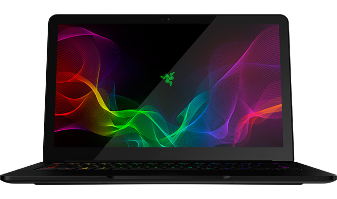
Besides shipping with Intel's Core i7-8550U, the updated Razer Blade Stealth 13.3” also comes standard with 16 GB of LPDDR3-2133 memory, as well as a 512 GB PCIe 3.0 x4 SSD. The laptop also retains support for Thunderbolt 3 and eGFX, allowing the integrated Intel UHD Graphics 620 to be augmented with AMD Radeon and NVIDIA GeForce video cards in an eGFX chassis. In either scenario, the upgraded Blade Stealth has the same 13.3” IGZO panel with a 3200×1800 resolution (QHD+), 400 nits brightness and offering 100% sRGB color gamut coverage as the model released in June.
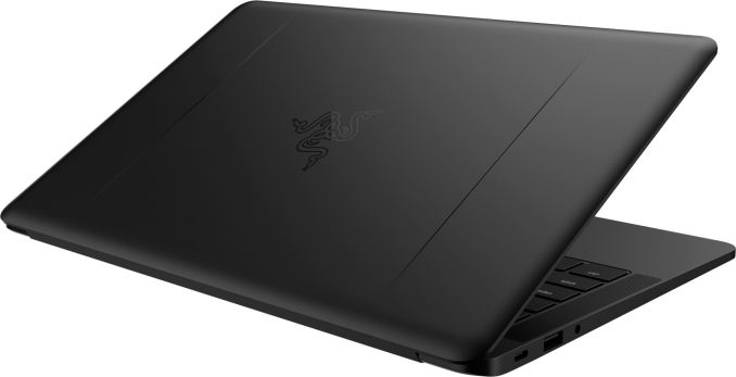
Coming off of the heels of Intel's dual-core Kaby Lake-U CPUs, the big draw for the new Kaby Lake Refresh-U CPUs is of course the additional two CPU cores. For moderately-to-heavily threaded workloads that can use more than two cores, these newer quad-core CPUs can offer a sizable boost in performance. Interestingly, Razer also claims that the new version of the laptop has a longer battery life, despite the fact that the battery size is unchanged. That said, Razer hasn't left the laptop's chassis completely untouched; the quad-core Blade Stealth is slightly thicker than the predecessor, adding another 0.7mm over its predecessor.
Otherwise when it comes to connectivity, the updated Blade Stealth 13.3” has all the same features as its predecessor does: a Killer Wireless AC 802.11ac + Bluetooth 4.1 module, an Intel Thunderbolt 3 controller supporting one USB Type-C port, two USB 3.0 connectors, an HDMI 2.0a display output, a 720p webcam, a TRRS audio port, an RGB-backlit Razer Chroma keyboard and so on. The system is equipped with the same 53.6 Wh lithium-ion polymer battery as the previous model, but Razer claims that the upgraded Blade Stealth can now last for 10 hours on one charge. In addition, the machine comes with a 65 W USB-C power adapter (up from 45 W for the earlier models) which hopefully means that it will also charge faster.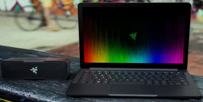
The new quad-core Razer Blade Stealth 13.3" comes in CNC-milled aluminum chassis in black or gunmetal gray finish, but the chassis is 0.7 mm/0.02" thicker than the chassis used for the dual-core Blade Stealth 13.3". The new system in its default configuration (see the table above) is available for $1,699 from RazerStore.com in the U.S., Canada, France, United Kingdom, and Germany. This is a bit higher than the price of the older dual-core version, but Razer does not offer the new model with a 256 GB SSD, so the new model has higher baseline specifications.Razer Blade Stealth Laptops: Fall 2017, Default Configurations 13.3"/QHD+
Quad-Core13.3"/QHD+
Dual-Core12.5"/4K
Dual-CoreDisplay Diagonal 13.3" 12.5" Resolution 3200×1800 3840×2160 Brightness 400 cd/m² unknown CPU Core i7-8550U
4C/8T
1.8 GHz/4 GHz
8 MB LLC
15 WCore i7-7500U
2C/4T
2.7 GHz/3.5 GHz
4 MB LLC
15 WGraphics Intel HD Graphics 620 RAM Capacity 16 GB Type LPDDR3-2133 LPDDR3-1866 Storage 512 GB SSD 256 GB SSD 512 GB/1 TB SSD Wi-Fi Killer 802.11ac Wi-Fi module Bluetooth 4.1 USB 2 × USB Type-A Thunderbolt 1 × Thunderbolt 3 port (USB Type-C) Other I/O HDMI 2.0a, 720p webcam, TRRS connector for audio, speakers, microphone Dimensions Height 13.8 mm/0.54" 13.1 mm/0.52" Width 321 mm/12.6" Depth 206 mm/8.1" Weight 1.35 kg
2.98 lbs1.33 kg
2.93 lbs1.29 kg
2.84 lbsBattery Life 10 hours Price $1699 $1399 $1349/$1749
On that note, it should be pointed out that the new quad-core version of the laptop adds to the existing Stealth family, rather than replacing it wholesale. The company and its partners also offer previous-gen Blade Stealth 13.3”/QHD+ laptops: the entry-level Blade Stealth with a 256 GB SSD is now available for $1349.99, whereas the higher-end Blade Stealth with a 1 TB SSD can be obtained with $1699.
Buy Blade Stealth 13.3: Core i7-7500U, 16 GB RAM, 1 TB SSD on Amazon.com
It is noteworthy that Razer is not upgrading the 12.5” version of the Blade Stealth that features a 4K UHD display, and it looks like this is a deliberate decision. The key feature of this notebook is its 4K UHD display that offers among the highest pixel density (for a laptop) in the industry, and along those lines the even smaller laptop isn't a great fit for the higher performing quad-core CPUs; at least not without some sacrifices to size or throttling.
Related Reading: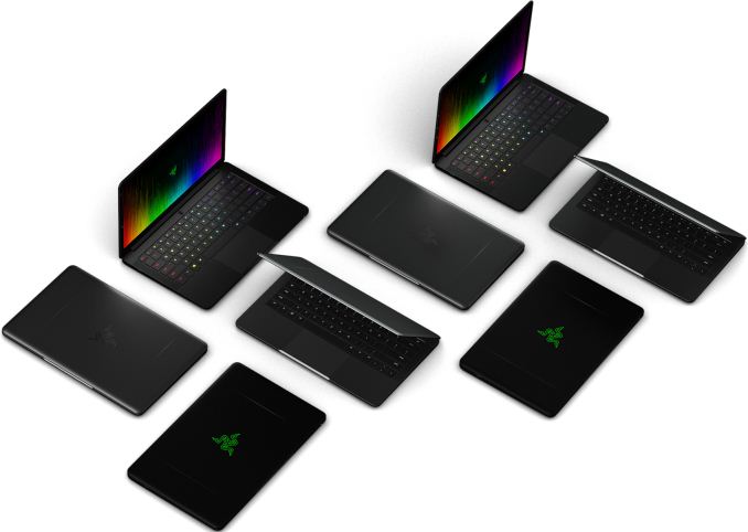
- Razer Updates The Razer Blade Stealth: More Screen, Less Bezel, New Color Option
- Razer Reveals New Blade Pro: GTX 1060 Graphics, Full HD, Lower Price Point
- Razer Blade Gets Core i7-7700HQ, Adds 4K Touchscreen, 1 TB SSD Options
- The 2016 Razer Blade Pro Review
- Razer Updates The Razer Blade Pro With THX Certification
More...
-
10-18-17, 02:22 PM #7437
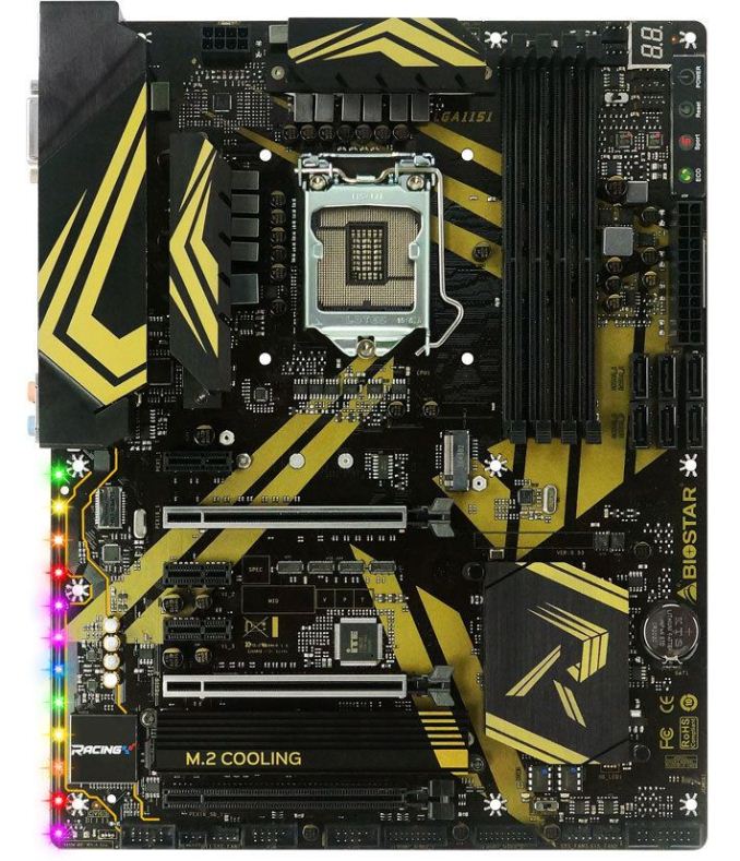
Anandtech: Biostar Announces Z370GT7 and Z370GT6 Motherboards for Coffee Lake CPUs
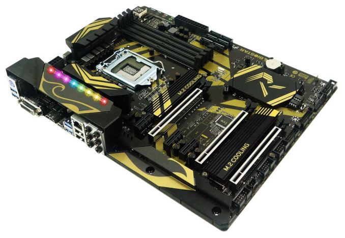
Not willing to be left behind at the starting line, Biostar has announced its entries into the rapidly growing Z370 motherboard market. At the time of publication, Biostar is bringing two boards to the table from their Racing line with the Z370GT7 and Z370GT6. The GT7 is the company's flagship board and, accordingly, will be the more expensive of the two. While both are full-featured motherboards, the GT7 offers an additional M.2 heatsink over the GT6 (bringing the total to two), three full-length PCIe slot reinforced compared to the GT6's two, as well as additional shrouding covering the audio section of the board on the GT7. Outside of that, differences between the boards will be difficult to spot.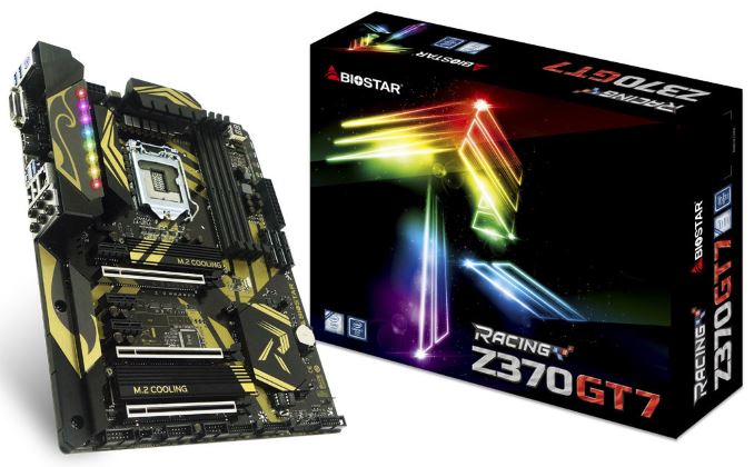
The Biostar Racing line is in its third generation Racing series aesthetic which features a gold and black color theme. All heatsinks on the board are black and adorned with yellow accents while the PCB itself is black. The “R” (Racing) symbol is found prominently on the chipset heatsink. Other gold accents are found scattered around the board.
Both boards use a 10-phase VRM to drive the Coffee Lake-based CPUs. Both boards also feature three full-length PCIe x16 slots and three x1 slots. In the top right corner, both boards have a debug LED, BIOS switch, and a panel with four buttons on it for power/reset functionality, as well as Turbo and Eco mode buttons. RGB LEDs can be found on both boards with the GT7’s located on the back panel IO shroud, while the GT6’s are found on to the left of the audio section. The integrated LEDs and external LEDs (via two headers) can be controlled with Biostar’s Vivid LED DJ utility. It features 10 different flashing modes along with color, speed, and brightness controls allowing control over each lighting zone independently.
Neither board uses reinforced DIMM slots, however two full-length PCIe slots on the GT6 and all three slots on the GT7 get protection. The slots break down to x8/x8/x4 and both boards support 3-way AMD Crossfire, though it should be noted that there isn’t a mention of SLI support in any form on the specifications page. The last full-length slot at x4 shares bandwidth with the second M.2 slot. The boards four DIMM slots support up to 64GB of RAM with speeds supported to DDR4 3866(OC). While still fast, this is the second lowest speed we have seen supported across all Z370 boards covered. Only the ECS board supported slower maximum speeds (DDR4 3200).
For mass storage purposes, both boards use the full allotment of six chipset managed SATA ports. However iInstead of locating these in their typical position to the right of the PCH heatsink on the bottom half of the board, Biostar as placed them towards the middle of the board oriented them vertically. The first M.2 slot is above the top full-length PCIe slot and supports up to 80mm sticks, while the second slot can be found between the bottom two PCIe slots and supports up to 110mm devices. The GT7 offers heatsinks on both M.2 slots, while the GT6 only cools the bottom slot.
As for cooling, the board gives users a total of five four-pin fan headers to use scattered in various locations around the board. These can be controlled via voltage or PWM through the BIOS or through the Windows-based application. Audio functionality is handled by the Realtek ALC1220 codec, uses EMI shielding, what looks to be Chemicon audio caps, as well as separation from the rest of the board. Network capabilities on both boards and handled by the Intel I219-V Gigabit Ethernet which supports LAN surge protection.
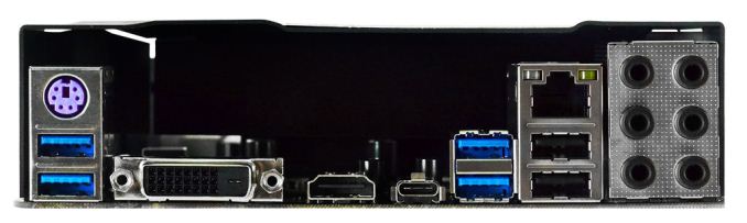
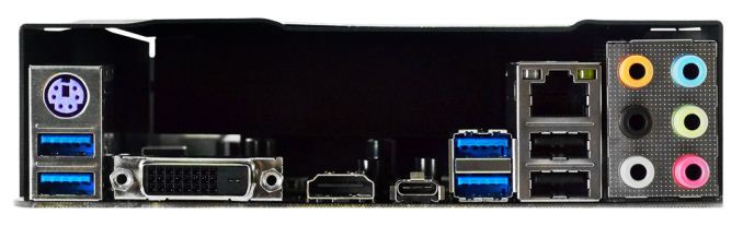
Both the GT6 and GT7 have the same number and types of USB ports. There are two USB 3.1 (5 Gbps) Type-A ports and one Type-C, and an additional two USB 2.0 ports on the back panel IO. Internally there is an additional USB 3.1 (5 Gbps) header and USB 2.0 header for front panel connections. The back panel IO also contains a PS/2 port, DVI-D and HDMI for video outputs, as well as a six plug audio stack. The GT7 chooses to use all black colored plugs versus the GT6 using the color-coded version most are familiar with.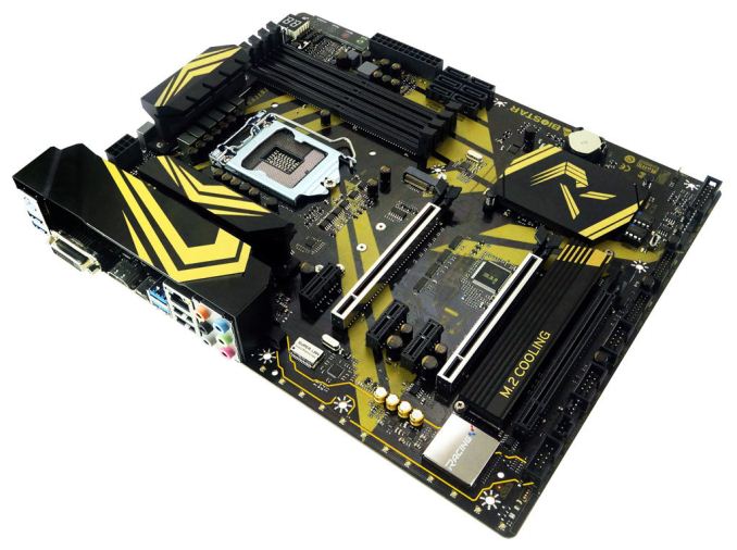
Biostar Z370GT6 & Z370GT7 Warranty Period 3 Years Product Page Z370GT6 / Z370GT7 Price N/A Size ATX CPU Interface LGA1151 Chipset Intel Z370 Express Memory Slots (DDR4) Four DDR4
Supporting 64GB
Dual Channel
Support DDR4 3866(OC)Network Connectivity 1 x Intel I219-V LAN Onboard Audio Realtek ALC1220 PCIe Slots for Graphics (from CPU) 2 x PCIe 3.0 x16 slots @ x8
1 x PCIe 3.0 x16 slots @ x4PCIe Slots for Other (from Chipset) 3 x PCIe 3.0 x1 slots @ x1 Onboard SATA 6 x Supporting RAID 0/1/5/10 Onboard SATA Express None Onboard M.2 2 x PCIe 3.0 x4 - NVMe or SATA Onboard U.2 None USB 3.1 2 x Type-A (10 Gbps) Back Panel
1 x Type-C (10 Gbps) Back Panel
2 x Type-A (5 Gbps) Back Panel
2 x HeaderUSB 3.0 N/A USB 2.0 2 x Ports Back Panel
2 x HeaderPower Connectors 1 x 24-pin EATX
1 x 8-pin ATX 12VFan Headers 2 x CPU
3 x System
(PWM and DC Controlled)IO Panel 1 x PS.2 keyboard/mouse port
2 x USB 3.1 G2 ports
1 x USB 3.1 Type-C
2 x USB 3.1 Type-A
1 x HDMI
1 x DVI-D
2 x RJ-45 LAN Port
5 x Audio Jacks
Related Reading:
More...
-
10-19-17, 08:11 AM #7438
Anandtech: Intel Documents Point to AVX-512 Support for Cannon Lake Consumer CPUs
A new update to the Intel document for software developers indicates that the company will begin to introduce various AVX-512 instruction set extensions to its consumer CPUs soon. This will start from the codenamed Cannon Lake (CNL) and Ice Lake (ICL) processors, made using 10 nm process technologies. The new extensions will enable future chips to improve performance in certain applications. One of the main questions on AVX-512 is which consumer programs will actually support the AVX-512 when these CNL and ICL processors hit the market. In addition to the AVX-512, the upcoming processors will introduce a host of other new non-AVX-512 instructions.
Buy Intel Core i9-7900X on Amazon.com
AVX-512 Coming to Consumer CPUs
According to the Intel Architecture Instruction Set Extensions and Future Features Programming Reference document, Intel’s Cannon Lake CPUs will support AVX512F, AVX512CD, AVX512DQ, AVX512BW, and AVX512VL. This will bring the feature set of these CPUs to the current level of the Skylake-SP based processors. In addition, the Cannon Lake microarchitecture will support the AVX512_IFMA and AVX512_VBMI commands, but at this point, it is unclear whether the support will be limited to servers, or will also be featured in the consumer processors (the latter scenario is likely based on the document wording, but remains unclear).
Intel originally promised to release Cannon Lake processors in 2016 – 2017 timeframe, but delayed introduction of its 10 nm process technology to 2018, thus postponing the CPU launch as well. Initially it was expected that the Cannon Lake CPUs would generally resemble the Kaby Lake and Coffee Lake chips with some refinements, but the addition of the AVX-512 support means a rather tangible architecture improvement. For AVX-512, large the chunks of data require massive memory bandwidth, which the Skylake-SP cores get due to large caches and more memory controllers. Keeping in mind memory bandwidth and power consumption factors, the AVX-512 might not be supported by all Cannon Lake client CPUs, but only by those aimed at higher-performance machines (i.e., no AVX-512 for ULP mobile parts as well as entry-level desktop SKUs, but this is a speculation at this point). Meanwhile, a good news is that by the time AVX-512-supporting Cannon Lake processors arrive, programs for client PCs that take advantage of the latest extensions will likely be available.
The evolution of the AVX-512 on general-purpose CPUs is not going to stop. Intel’s Ice Lake processors will support AVX512_VPOPCNTDQ (which will also be supported by the Xeon Phi ‘Knights Mill’) commands as well as AVX512_VNNI, AVX512_VBMI2, AVX512+VPCLMULQDQ and AVX512_BITALG instructions. The ICL chips will also feature AVX-512 versions of known AES and GFNI algorithms for encryption and error corrections — AVX512+VAES and AVX512+GFNI.
Meanwhile, the Knights Mill will exclusively support AVX512_4FMAPS and AVX512_4VNNI (at least for a while, because an Intel filing with the Linux kernel states that the upcoming Xeon Phi and Xeon CPUs will support both commands, but descriptions of Linux patches are not always accurate, plus, plans tend to change).
As it turns out from Intel’s document, the Cannon Lake and Ice Lake processors will have an up-to-date AVX-512 support. It is unknown whether the CNL and the ICL cores will be used inside the future server processors (remember that Intel has server-specific 'Cascade Lake' product incoming), but if this is the case, then it looks like Intel’s cores for server and client computers will have the same feature-set going forward, at least when it comes to the AVX-512 support.AVX-512 Support Propogation by Various Intel CPUs Xeon, Core X General Xeon Phi Skylake-SP AVX512BW
AVX512DQ
AVX512VLAVX512F
AVX512CDAVX512ER
AVX512PFKnights Landing Cannon Lake AVX512VBMI
AVX512IFMAAVX512_4FMAPS
AVX512_4VNNIWKnights Mill Ice Lake AVX512_VNNI
AVX512_VBMI2
AVX512_BITALG
AVX512+VAES
AVX512+GFNI
AVX512+VPCLMULQDQAVX512_VPOPCNTDQ Source: Intel Architecture Instruction Set Extensions and Future Features Programming Reference (pages 12 and 13)
Adding the AVX-512 to consumer processors looks like an important development even though the instruction set was primarily designed to process large amounts of data common for servers and, to a degree, workstations (such as encoding, rendering, cryptography, deep learning, etc.). Apparently, Intel believes that 512-bit INT/FP calculations will be important for mainstream PCs as well. A big question is how exactly Intel plans to implement the AVX-512 in various Cannon Lake and Ice Lake processors going forward. Keep in mind that Intel’s six and eight-core Skylake-X CPUs officially support one fused FMA for AVX-512-F, but the chips with 10+ cores officially support dual 512-bit AVX-512-F ports and can offer up to two times higher performance. So in that respect, there is potential for further differentiation between products.
In the meantime, Intel’s Cannon Lake and Ice Lake CPUs will have a number of other new instructions for various matters and they are certainly worth looking at.
New Instructions to Improve Security, Performance of Upcoming CPUs
In a bid to speed up certain cryptography algorithms, Cannon Lake will feature the SHA-NI instruction set that is already supported by the Goldmont cores. SHA-NI is of a similar base to AES-NI, that was added several generations prior. Based on Intel’s publications, SHA-NI can speed up SHA1, SHA256 and SHA224 algorithms. In addition, the new CPUs will also support the UMIP security mechanism that prevents the execution of certain instructions in if their privilege level is insufficient for that, preventing certain apps from accessing the OS settings.
The Ice Lake chips will bring support for Fast Short REP MOV instruction that will enable fast moves of large amounts of data from one location to another, which will benefit optimized memory-intensive applications. Keep in mind that we are moving towards persistent memory for a number of server applications and therefore large amounts of data located in DRAM and/or NVDIMMs will be more common in the future.
Another interesting feature supported by the Ice Lake consumer processors is CLWB (Cache Line Write Back) command for NVMe programming. The feature is already supported by the Skylake-SP cores and is required to better handle SSDs connected to the processor, but will come into consumer products with Ice Lake. CLWB flushes the write caches, but does not invalidate the data, making it available if it is needed after the line is flushed, thus improving performance in certain situations. Given the Purley/Skylake-SP context, CLWB is something required for upcoming NVDIMMs (based on 3D XPoint), but it is not completely clear how Intel expects to use it in case of consumer platforms (they make sense for certain workstation applications and for that reason CLWB is supported by SKL-SP). In any case, the addition of CLWB will add some speed in certain cases when very fast SSDs are used and cache miss is an issue.
There are other features coming in the Goldmont Plus (the heart of upcoming Gemini Lake SoCs) and Ice Lake processors, namely PTWRITE and RDPID, which seem to be aimed mostly at software developers and which purpose may not benefit end users right away.
Some HistoryInstruction Set Extensions of Cannon Lake, Ice Lake and Goldmont+ CPUs Instruction Purpose Description Cannon Lake SHA-NI Security Cryptography acceleration. UMIP
User-Mode Instruction PreventionSecurity Prevents execution of certain instructions if the Current Privilege Level (CPL) is greater than 0. If these instructions were executed while in CPL > 0, user space applications could have access to system-wide settings such as the global and local descriptor tables, the task register and the interrupt descriptor table. Ice Lake CLWB
Cache Line
Write BackPerformance Writes back modified data of a cache line similar to CLFLUSHOPT, but avoids invalidating the line from the cache (and instead transitions the line to non-modified state). CLWB attempts to minimize the compulsory cache miss if the same data is accessed temporally after the line is flushed if the same data is accessed temporally after the line is flushed. Fast Short REP MOV Performance Enables fast moves of data from one location to another. RDPID
Read Processor IDGeneral Quickly reads processor ID to discover its feature set and apply optimizations/use specific code path if possible. Goldmont Plus PTWRITE
Write Data to a Processor Trace PacketDebugging Unclear. UMIP Security See above RDPID General See above Source: Intel Architecture Instruction Set Extensions and Future Features Programming Reference (pages 12 and 13)
Intel and AMD have been adding various instruction set extensions to the x86 architecture since the mid-1990s. Throughout the recent 20 years, both companies have brought in hundreds of new instructions designed to improve performance in various applications by SIMD instructions and feeding CPU cores large amounts of data at once or by using special-purpose hardware. Intel’s latest mainstream extensions are called the AVX/AVX2 and their main purposes were increasing the width of the register file (both SIMD and integer) to 256 bits and the introduction of commands like the FMA3 (that serves the same purpose — does relatively complex computations in one instruction). To perform 256-bit AVX2 operations, CPUs have to lower their frequency to maintain stability, as cores tend to draw a lot of power under such workloads, but even at lower clock rates AVX/AVX2 make a lot of sense and increase overall throughput.
The next step in the evolution of the instruction set extensions that Intel made was the AVX-512. With AVX-512 the company decided to introduce different sets of instructions for different applications and implemented them in different products. Some of the AVX-512 extensions are aimed primarily at enterprise workloads, whereas the others are needed for supercomputers or high performance compute. Implementing all of them in in all products hardly makes a lot of sense for Intel and its customers, so the latest Skylake-SP Xeons (and the high-end desktop processors) support one set of AVX-512 commands and the Xeon Phis support another one. In the meantime, contemporary mainstream consumer CPUs do not support AVX-512 at all. One of the reasons for this is because the physical implementation significantly increases die size (by up to 15% in case of the Skylake core). Other factors such as the cost associated with a die increase, and partly because client applications today cannot take advantage of such instructions, are also in the mix. In the future, this is going to change as Intel plans to enable support of certain AVX-512 variations in its future Cannon Lake and Ice Lake processors for mainstream consumers.
Wrapping Up
The addition of the AVX-512 to the future consumer CPUs is a good news for those who use such processors for things like video encoding, rendering or other applications that are common for workstations. Meanwhile, with the Ice Lake consumer chips, Intel is adding a deep learning-specific (AVX512_VNNI) 512-bit instructions as well as the NV-DIMM-oriented features such as CLWB, although immediate advantages for this market segment are unclear. Intel is opening this information up to allow developers to prepare for these processors and develop software in advance. In any case, all new features are always welcome by many because at some point they start to bring certain advantages.
Related Reading- The Intel Skylake-X Review: Core i9 7900X, i7 7820X and i7 7800X Tested
- The Intel Skylake-X Microarchitecture Analysis: Adding in AVX512 and Tweaks to Skylake-X
- Intel Launches Xeon-W CPUs for Workstations: Skylake-SP & ECC for LGA2066
- Hot Chips: Intel Knights Mill Live Blog
Source: Intel (via WikiChip Twitter).
More...
-
10-19-17, 08:11 AM #7439
Anandtech: HighPoint RocketStor RS6114V 4-Bay USB-C RAID Enclosure Review
Storage enclosures come in many varieties to target different market segments. They usually have one or more downstream SATA ports, with USB being a popular interface in the low-end and mid-range markets. Within the USB storage enclosure market, device vendors have multiple opportunities to tune their product design for specific use-cases. Today's review will take a look at HighPoint's RocketStor RS6114V, a 4-bay direct-attached storage enclosure backed up by their software RAID stack.?
More...
-
10-19-17, 10:11 AM #7440
Anandtech: Samsungs 8LPP Process Technology Qualified, Ready for Production
Samsung this week announced that its 8LPP fabrication process, which it formally introduced earlier this year, had passed qualification tests. The manufacturing technology will be used to produce advanced SoCs next year and will be Samsung’s final leading edge process based solely on DUV lithography before the company adopts EUV for select layers with its 7LPP process node.
The 8LPP fabrication technology is an evolution of Samsung’s 10 nm node that uses narrower metal pitches and promises a 10% area reduction (at the same complexity) as well as a 10% lower power consumption (at the same frequency and complexity) compared to the 10LPP process. Samsung does not disclose which standard cell libraries are used by the 8LPP, but the 10LPP relies on 8.75T and 10.5T, so it is logical to expect the 8LPP to use similar ones. Samsung does not disclose whether the 8LPP relies on quadruple patterning techniques, or if it continues to use triple patterning like the company’s 10LPE/10LPP processes, but QPT is an option to shrink die sizes at the increase in cost (and potential defects).
Samsung plans to use the 8LPP manufacturing technology to produce SoCs for various applications, including smartphones, cryptocurrency and networks/servers, but does not elaborate on exact designs or clients. The only thing we do know is that Qualcomm will be one of the first customers to adopt the 8LPP and that the company expects the new technology to ramp up fast (which possibly means that it uses the same libraries and manufacturing equipment as the 10 nm nodes).Advertised PPA Improvements of New Process Technologies
Data announced by companies during conference calls, press briefings and in press releases14LPP
vs 28LPP10LPE
vs 14LPE10LPE
vs 14LPP10LPP
vs 10LPE10LPU
vs
10LPE8LPP
vs 10LPPPower 60% 40% 30% ~15% ? 10% Performance 40% 27% >10% ~10% ? ? Area Reduction 50% 30% 30% none ? 10%
“8LPP will have a fast ramp since it uses proven 10 nm process technology while providing better performance and scalability than current 10nm-based products” said RK Chunduru, a senior vice president of Qualcomm.
Neither Samsung nor Qualcomm are disclosing when they expect to ship their first 8LPP chips, but since the technology has passed qualification tests (meaning that quality and reliability of ICs made using the technology meet certain guidelines, such as those proposed by JEDEC), we would expect the SoCs to arrive in the coming quarters.
Related Reading- Samsung and TSMC Roadmaps: 8 and 6 nm Added, Looking at 22ULP and 12FFC
- GlobalFoundries Adds 12LP Process for Mainstream and Automotive Chips; AMD Planning 12LP CPUs & GPUs
- GlobalFoundries Details 7 nm Plans: Three Generations, 700 mm², HVM in 2018
More...


 Quote
Quote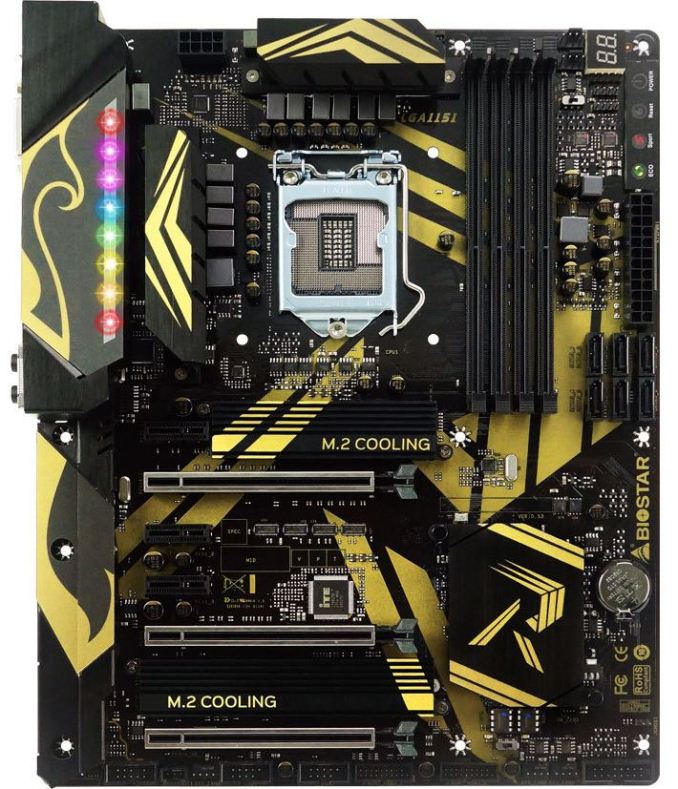
Thread Information
Users Browsing this Thread
There are currently 44 users browsing this thread. (0 members and 44 guests)


Bookmarks