

Results 7,501 to 7,510 of 12095
Thread: Anandtech News
-
11-08-17, 07:12 AM #7501
Anandtech: SanDisk Extreme and Extreme PRO Memory Cards Review
Digital cameras and camcorders employ memory cards (flash-based removable media) for storage of captured content. There are different varieties of memory cards catering to various performance levels. CompactFlash (CF) became popular in the late 90s, but, has now been overtaken by Secure Digital (SD) cards. Many computing systems (PCs as well as smartphones) also support SD cards for augmenting local storage capabilities. High-end recording systems with fast storage requirements use CFast and/or XQD cards. We recently started in-depth evaluation of the performance of various memory cards. SanDisk sent us a representative bunch of their memory card portfolio for review. Read on for a look at some of their memory cards.
More...
-
11-08-17, 08:18 AM #7502
Anandtech: Samsung Offers Free DeX Station or Gear VR with Galaxy S8, Galaxy Note8
Samsung has kicked off a new promotional campaign that bundles either of the company's two major smartphone peripherals – the DeX station or the Gear VR headset – with the company’s latest smartphones. The move enables Samsung to increase sales of its hardware and popularize its smartphone-based productivity as well as VR platforms.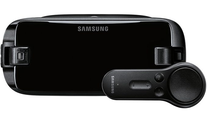
For a limited time, Samsung is bundling a DeX or a Gear VR with its Galaxy S8, Galaxy S8+, Galaxy S8 Active, as well as Galaxy Note8 smartphones purchased directly from Samsung.com. The manufacturer normally charges $99 for the DeX station and $129 for the Gear VR, so the promo campaign makes a lot of sense for those who had plans to get one of the devices. There are certain terms and conditions to be met, but the main one is to buy one of the aforementioned smartphones directly from Samsung and include one of the devices into the cart before making the purchase.
This is not the first time when Samsung is bundling DeX or Gear VR with its new smartphones, but it is noteworthy that the company is re-launching the campaign in the middle of the Galaxy S8’s life cycle and ahead of the holiday season. By offering free DeX or GearVR hardware with its latest smartphones, Samsung is killing two birds with one stone. Firstly, it sells a high-end smartphone. Secondly, it popularizes its productivity and VR platforms.
The DeX may not look like a big deal at the moment, but it is an important effort for the company. At present, the DeX allows to run select apps on the big screen and use a keyboard and a mouse to control them. In the future, Samsung plans to enable users to run various Linux applications on its smartphones (through its Linux on Galaxy app), essentially bringing a host of productivity programs to its platform and creating a rival to Microsoft’s Continuum.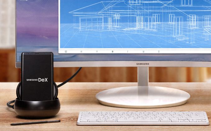
Meanwhile, the Gear VR is a strong contender to be the most popular VR platform and offering it for free to owners of advanced smartphones means getting new customers that are willing to pay for content. Samsung’s sales of the Gear VR headsets in Q2 2017 totaled 568,000 units, leaving behind headsets from Sony, Oculus VR, HTC and others, according to IDC. Analysts from the latter believe that bundle deals greatly help Samsung to drive adoption of the Gear VR and therefore it is logical for the company to run various promotions, especially as new contenders are either entering the scene, or are about to.
Related Reading:
- HTC Offers Vive + GeForce GTX 1070 + Fallout 4 VR Bundle for $799
- Oculus Announces Oculus Go: Untethered VR For $199 USD
- Dell’s Visor Available for Pre-Order: A Mixed Reality Headset, Ships in Mid-October
- Dell Enters VR Arena With "Visor" HMD
- HTC Announces Snapdragon 835-Based VIVE VR Headset for Chinese Market
- HTC Permanently Cuts Price of Vive to $599
- HTC Announces New Standalone Vive VR Headset with Google Daydream Support
Source: Samsung (via Notebookcheck.net)
More...
-
11-08-17, 05:14 PM #7503
Anandtech: Intel to Develop Discrete GPUs, Hires Raja Koduri as Chief Architect
On Monday, Intel announced that it had penned a deal with AMD to have the latter provide a discrete GPU to be integrated onto a future Intel SoC. On Tuesday, AMD announced that their chief GPU architect, Raja Koduri, was leaving the company. Now today the saga continues, as Intel is announcing that they have hired Raja Koduri to serve as their own GPU chief architect. And Raja's task will not be a small one; with his hire, Intel will be developing their own high-end discrete GPUs.
Starting from the top and following yesterday’s formal resignation from AMD, Raja Koduri has jumped ship to Intel, where he will be serving as a Senior VP for the company, overseeing the new Core and Visual Computing group. As a chief architect and general manager, Intel is tasking Raja with significantly expanding their GPU business, particularly as the company re-enters the discrete GPU field. Raja of course has a long history in the GPU space as a leader in GPU architecture, serving as the manager of AMD’s graphics business twice, and in between AMD stints serving as the director of graphics architecture on Apple’s GPU team.
Meanwhile, in perhaps the only news that can outshine the fact that Raja Koduri is joining Intel, is what he will be doing for Intel. As part of today’s revelation, Intel has announced that they are instituting a new top-to-bottom GPU strategy. At the bottom, the company wants to extend their existing iGPU market into new classes of edge devices, and while Intel doesn’t go into much more detail than this, the fact that they use the term “edge” strongly implies that we’re talking about IoT-class devices, where edge goes hand-in-hand with neural network inference. This is a field Intel already plays in to some extent with their Atom processors on the GPU side, and their Movidius neural compute engines on the dedicated silicon sign.
However in what’s likely the most exciting part of this news for PC enthusiasts and the tech industry as a whole, is that in aiming at the top of the market, Intel will once again be going back into developing discrete GPUs. The company has tried this route twice before; once in the early days with the i740 in the late 90s, and again with the aborted Larrabee project in the late 2000s. However even though these efforts never panned out quite like Intel has hoped, the company has continued to develop their GPU architecture and GPU-like devices, the latter embodying the massive parallel compute focused Xeon Phi family.
Yet while Intel has GPU-like products for certain markets, the company doesn’t have a proper GPU solution once you get beyond their existing GT4-class iGPUs, which are, roughly speaking, on par with $150 or so discrete GPUs. Which is to say that Intel doesn’t have access to the midrange market or above with their iGPUs. With the hiring of Raja and Intel’s new direction, the company is going to be expanding into full discrete GPUs for what the company calls “a broad range of computing segments.”
Reading between the lines, it’s clear that Intel will be going after both the compute and graphics sub-markets for GPUs. The former of course is an area where Intel has been fighting NVIDIA for several years now with less success than they’d like to see, while the latter would be new territory for Intel. However it’s very notable that Intel is calling these “graphics solutions”, so it’s clear that this isn’t just another move by Intel to develop a compute-only processor ala the Xeon Phi.
NVIDIA are at best frenemies; the companies’ technologies complement each other well, but at the same time NVIDIA wants Intel’s high-margin server compute business, and Intel wants a piece of the action in the rapid boom in business that NVIDIA is seeing in the high performance computing and deep learning markets. NVIDIA has already begun weaning themselves off of Intel with technologies such as the NVLInk interconnect, which allows faster and cache-coherent memory transfers between NVIDIA GPUs and the forthcoming IBM POWER9 CPU. Meanwhile developing their own high-end GPU would allow Intel to further chase developers currently in NVIDIA’s stable, while in the long run also potentially poaching customers from NVIDIA’s lucrative (and profitable) consumer and professional graphics businesses.
To that end, I’m going to be surprised if Intel doesn’t develop a true top-to-bottom product stack that contains midrange GPUs as well – something in the vein of Polaris 10 and GP106 – but for the moment the discrete GPU aspect of Intel’s announcement is focused on high-end GPUs. And, given what we typically see in PC GPU release cycles, even if Intel does develop a complete product stack, I wouldn’t be too surprised if Intel’s first released GPU was a high-end GPU, as it’s clear this is where Intel needs to start first to best combat NVIDIA.
(This Is Breaking News; More To Follow)
Source: Intel
More...
-
11-09-17, 08:26 AM #7504
Anandtech: Compulab Launches the Fitlet2 Passive SFF PC with Apollo Lake SoCs
Compulab has announced its new fitlet2 ultra-compact PC designed for a broad range of applications, including office, IoT and industrial. The Compulab fitlet2 is a small unit, cooled passively using its own chassis made of die-cast metal. The system supports Compulab’s function and connectivity extension T-cards (FACET cards) that add functionality, such as extra GbE or USB ports, or even a 4G modem.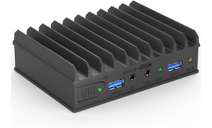
The Compulab fitlet2 measures 112 mm by 84 mm, meaning that it is smaller than Intel’s NUCs and other UCFF-class PCs. Depending on exact model, the Compulab fitlet2 can be based on Intel’s Atom x7-E3950, Atom x5-E3930 or a Celeron J3455, all based on Intel's Apollo Lake cores. The motherboard of the system features one SO-DIMM slot for up to 16 GB og DDR3L-1866 memory. As for storage options, the mainboard supports M.2-2260/2242 SSDs, modular M.2 eMMC drives as well as 2.5” SATA storage solutions. One M.2 module and one 2.5" drive can be installed at the same time.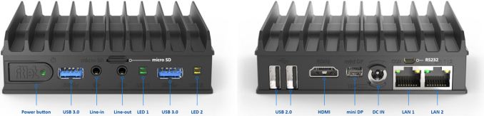
By default, the Compulab fitlet2 system comes with two GbE ports, two USB 3.0 connectors, two USB 2.0 headers, a COM port, audio jacks, a microSD slot, an HDMI 1.4, and an mDP 1.2 output. Users can install one of Compulab’s FACET cards to get other connectivity features, including (but not limited to) a 802.11ac Wi-Fi + Bluetooth 4.2 module, a 4G modem, two extra GbE ports, four additional USB headers, or an M.2 E-key slot. Compulab keeps the FACET spec open so interested parties can develop their own cards to extend I/O capabilities and address certain needs, such as FPGAs perhaps. One thing that should be kept in mind is that Apollo Lake SoCs only support PCIe 2.0, so the fitlet2 will not be able to take advantage of fast I/O or modern SSDs.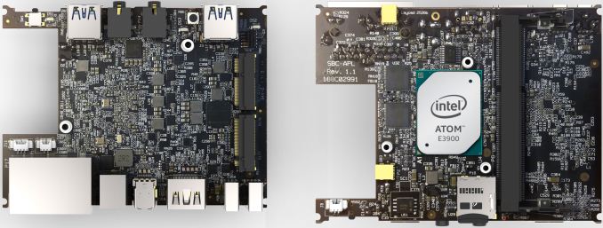
As mentioned above, the fitlet2 can be adapted for various applications and for this reason different versions of the PC will use slightly different enclosures. The low power models use 112 mm by 84 mm housing that is 25mm thick, while a higher performance SKU is 34 mm thick (to dissipate more heat), and industrial designs come in a 112x112x25 mm chassis because of mounting mechanisms.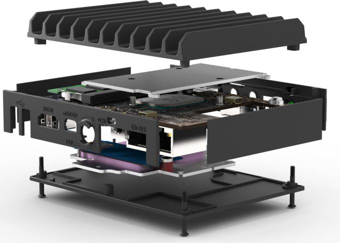
All versions of the fitlet2 are rated to operate in rather extreme environments with temperatures between -40°C and 85°C and humidity between 5% and 95% (non-condensing).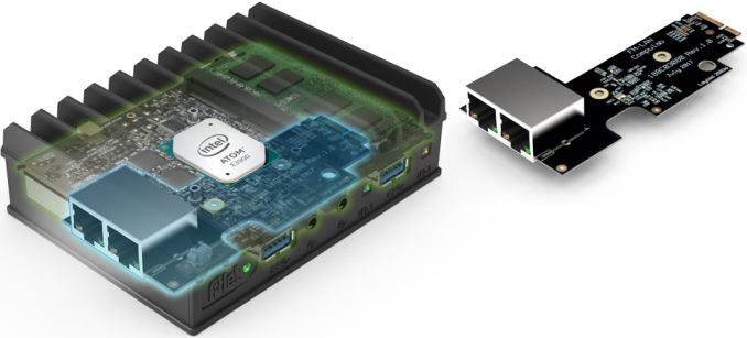
Gallery: Compulab Launches Fitlet2 SFF PC for IoT: All-Metal Chassis, Apollo Lake, Four GbE Ports, Extended TempsBrief Specifications of Compulab's fitlet2 Atom x7 Atom x5 Celeron CPU Atom x7-E3950
4C/4T
1.6 GHz / 2.0 GHz
2 MB L2
12 WAtom x5-E3930
2C/2T
1.3 GHz / 1.8 GHz
2 MB L2
6.5 WCeleron J3455
4C/4T
1.5 GHz / 2.3 GHz
2 MB L2
10 WPCH integrated Graphics HD Graphics 505
(18 EUs)Intel HD Graphics 500
(12 EUs)Memory One SO-DIMM slot, up to 16 GB of DDR3L-1866 Storage eMCC A modular eMMC storage device M.2 A SATA SSD in M.2-2260/M.2-2242 form-factor 2.5" A SATA 2.5" SSD or HDD Wi-Fi Intel 802.11ac + BT 4.2 (optional, comes on a FACET module) Ethernet Two Gigabit Ethernet with RJ45 connectors (Intel i211)
Two additional GbE connectors may be installed using a FACET moduleDisplay Outputs 1 × HDMI 1.4
1 × mDP 1.2Audio 3.5 mm audio in and audio out (Realtek ALC886) USB 2 × USB 3.0 Type-A
2 × USB 2.0 Type-A
Four additional USB 2.0 connectors may be installed using a FACET moduleDimensions Low-power: 112 mm × 84 mm × 25 mm
High-performance: 112 mm × 84 mm × 34 mm
Industrial: 112 mm × 112 mm × 25 mmPSU External, 9V to 36V VESA Mounts 75 mm/100 mm OS Windows 10 IoT Enterprise LTSB
Linux Mint
Compatible with other operating systems


Because the fitlet2 enables to build systems featuring different specifications, Compulab does not announce exact MSRPs for all the units, possibly because 99% of such PCs will be built-to-order (the manufacturer even offers color customization for large customers). The cheapest fitlet2 is available for $153, but once it is equipped according to requirements, its price will be considerably higher (keep in mind that industrial DIMMs and SSDs rated for extended temperatures cost more than consumer-class components). All fitlet2 computers are covered by a five-year warranty and are guaranteed to be available for 15 years.
Related Reading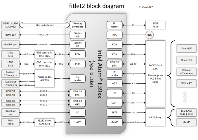
- ECS Quietly Adds PB01CF Ultra Compact PC to Lineup: a 5 Oz Apollo Lake Desktop
- ECS LIVA Z Fanless Dual-LAN Apollo Lake UCFF PC Review
- CES 2017: GIGABYTE Shows Passive Apollo Lake BRIX in Embedded UCFF
- Launch of Intel’s Apollo Lake NUCs Gets Closer as Intel Lists Them on Web Site
- ECS Preps LIVA Z: Apollo Lake-Based Nettop with 4K and USB-C Support
More...
-
11-09-17, 11:17 AM #7505
Anandtech: Intel Optane SSD DC P4800X 750GB Hands-On Review
Intel's rollout of Optane products, based on 3D XPoint memory, continues. Today is the release of the 750GB Optane SSD DC P4800X, a larger capacity version of the model launched earlier this year. Now Intel's flagship enterprise SSD family has a more useful capacity while offering the same chart-topping performance as the 375GB model that launched earlier this spring.
More...
-
11-09-17, 11:17 AM #7506
Anandtech: ASRock Releases X299 Taichi XE and X299 Gaming i9 XE: Big Boy Heatsinks
This week ASRock has released “XE” editions of two of its popular X299 motherboards: the X299 Taichi XE and the flagship X299 Professional Gaming i9 XE.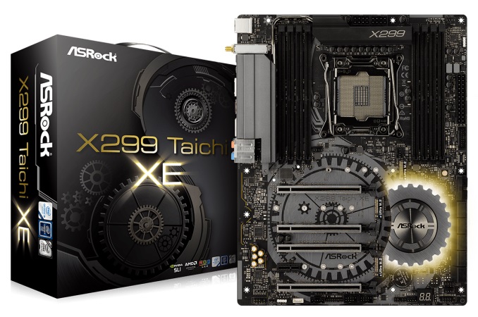
Buy ASRock X299 Taichi XE on Newegg
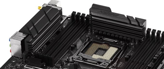
The XE versions have a larger main heatsink, and an additional power delivery heatsink connected via heatpipe located behind the back panel VRM. Along with being larger, there are more fins cut out increasing surface area and heat dissipation capabilities. The original(s) had a single, smaller heatsink to cool the 13-phase VRM underneath and not a lot of surface area. Both boards now also add a second 8-pin EPS 12V connector for additional power to the CPU. In order to fit the updated cooling solutions, the shroud covering the back panel IO and audio sections have been removed.
Buy ASRock X299 Professional Gaming i9 XE on Newegg
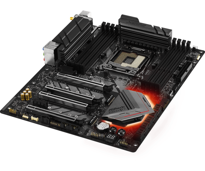
ASRock X299 Professional Gaming i9 (left)
ASRock X299 Professional Gaming i9 XE (right)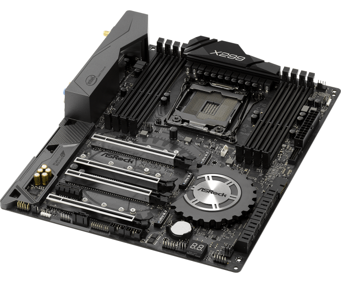
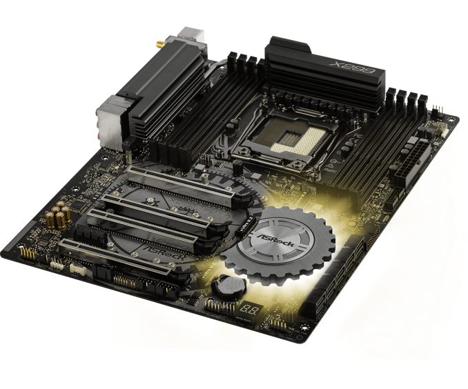
ASRock X299 Taichi (left)
ASRock X299 Taichi XE (right)
In the weeks after the Skylake-X and Basin Falls (X299) chipset release, concerns were brought up with the platform’s VRM and cooling. Igor Wallossek from Tom’s Hardware looked into this issue in depth. In the end, it was found that these 140W+ CPUs, such as the i9-7900X, can use around 250W when clocked around 4.5 GHz using all cores (through burn-in testing –a worst case scenario). All that power creates heat, both at the CPU and the VRM level delivering voltage to the FIVR. This was also a problem when motherboard manufacturers were implementing their own turbo modes over the top of Intel specifications.
The concern here there was that some motherboards do not have enough VRM cooling to dissipate the energy lost as heat from the power delivery. At base frequencies, in well ventilated cases, this doesn't appear to be a big issue, however some motherboard partners enable turbo-boosting features such as Multi Core Enhancement by default, raising clocks and voltages, and can be too aggressive with its enhancement. Of course, cooling a CPU using that amount of power isn’t as easy as strapping down a $30 air cooler on it and calling it "OK" either. The point is some motherboards in certain situations can throttle the CPU at the VRM level due to the heatsinks not being able to dissipate such loads.
While our X299 motherboard reviews have not shown much of this behavior so far (there have been other problems to solve), some motherboard partners have realized that improvements can be made in their implementations and have recently started announcing and releasing updated boards.
Pricing on the XE versions of the motherboards will cost a little bit more to compensate. The Taichi is currently priced at $289 on Newegg while the Taichi XE is $322. The Fatal1ty Gaming i9 is priced at $389 with the Gaming i9 XE at $422. Both boards are asking a $33 premium. If pushing 140W processors or the 165W flagship 7980XE hard is in the plans, one may want to consider the XE versions (ASUS has a Strix XE as well with a larger heatsink) and pay the premium, if only for peace of mind and cooler operation.
Related ReadingASRock Fatal1ty X299 Professional Gaming i9 XE and X299 Taichi XE Taichi XE Gaming i9 XE Warranty Period 3 Years Product Page Link Link Price Newegg US Newegg US Size ATX CPU Interface LGA2066 Chipset Intel X299 Memory Slots (DDR4) Eight DDR4
Supporting 128GB
Quad Channel
Up to 4400 MHzNetwork Connectivity 1 x Intel I219V GbE
1 x Intel I211AT GbE
1 x Intel AC3168 802.11ac Wi-Fi Module1 x Aquantia 10 Gigabit
1 x Intel I219V GbE
1 x Intel I211AT GbE
1 x Intel AC3168 802.11ac Wi-Fi ModuleOnboard Audio Realtek ALC1220 PCIe Slots for Graphics (from CPU) 44 Lane CPUs: x16, x16/x16, x16/x8/x16/x0, x8/x8/x16/x8 28 Lane CPUs: x16, x16/x8, x8/x8/x8, x8/x0/x8/x8 16 Lane CPUs: x16, x8/x0/x4x0 PCIe Slots for Other (from PCH) 1 x PCIe 3.0 x1 Onboard SATA Eight, RAID 0/1/5/10
Two Asmedia ASM1061Onboard SATA Express None Onboard M.2 3 x PCIe 3.0 x4 or SATA Onboard U.2 None USB 3.1 1 x Type-A
1 x Type-C
(ASMedia ASM3142 Controller)1 x Type-A
1 x Type-C
1 x Front Panel Type-C
(ASMedia ASM3142 Controller)USB 3.0 4 x Rear Panel
2 x via headers (ASM1074 Hub)USB 2.0 4 x via headers
2 x rear panelPower Connectors 1 x 24-pin ATX
1 x 8-pin CPUFan Headers 1 x CPU (4-pin)
1 x CPU Opt/Water Pump
2 x Chassis Fan
1 x Chassis Opt/Water PumpIO Panel 2 x Antenna Ports
1 x PS/2 Mouse/Keyboard Port
1 x Optical SPDIF Out Port
2 x USB 2.0 Ports
1 x USB 3.1 Type-A Port (10 Gb/s)
1 x USB 3.1 Type-C Port (10 Gb/s)
4 x USB 3.0 Ports
2 x RJ-45 LAN Ports
1 x BIOS Flashback Switch
1 x Clear CMOS Switch
HD Audio Jacks2 x Antenna Ports
1 x PS/2 Mouse/Keyboard Port
1 x Optical SPDIF Out Port
2 x USB 2.0 Ports
1 x USB 3.1 Type-A Port (10 Gb/s)
1 x USB 3.1 Type-C Port (10 Gb/s)
4 x USB 3.0 Ports
3 x RJ-45 LAN Ports
1 x BIOS Flashback Switch
1 x Clear CMOS Switch
HD Audio Jacks- The ASRock X299 Taichi Motherboard Review
- The ASRock Fatal1ty X299 Professional Gaming i9 Motherboard Review
- The Intel Skylake-X Review: Core i9 7900X, i7 7820X and i7 7800X Tested
- The Intel Core i9-7980XE and Core i9-7960X CPU Review Part 1: Workstation
More...
-
11-09-17, 01:42 PM #7507
Anandtech: Lite-On Launches CA3 M.2 NVMe SSDs: Up to 1TB, 2.9 GB/s, Marvell 88SS1093
Lite-On has quietly added its new high-end CA3 M.2 NVMe SSDs to its lineup. The new drives are based on Toshiba’s 3D TLC NAND memory, a Marvell controller, and are the fastest SSDs made by Lite-On to date. The company will sell the CA3 NVMe M.2 drives primarily to OEMs and PC makers, whereas consumers will have to wait until Plextor releases its M9Pe products.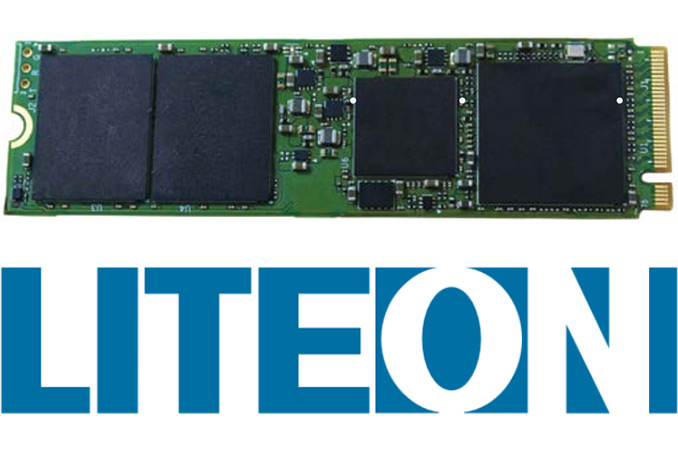
These new M.2 drives will use a Marvell controller featuring three Cortex R5 cores, 8 NAND channels with 4 CE per channel (32 targets in total) and supports Marvell’s third-gen ECC technology based on the LDPC algorithm. The Marvell 88SS1093/92 controllers are among the highest-performing consumer SSD controllers to date, so Lite-On’s choice for its high-end CA3 drives was obvious. Speaking of performance, the manufacturer promises up to 2900 MB/s sequential read speed and around 1200-1700 MB/s sequential write speed for the higher-end models when pSLC cache is used (the company separately mentions TLC write speed, see the table below for details). As for random performance, we are dealing with drives capable of up to 380K/260K read/write IOPS (1 TB version, others are slower). The power consumption of the new Lite-On drives will be up to 8 W, which means a fairly high heat dissipation and may not be suitable for mobile devices.
The Lite-On CA3 SSDs are rated for 1.5 million hours MTBF and come with a three-year warranty. For many retail drives, such ratings and warranty are considered low, but for OEMs they are standard. Since Lite-On traditionally sells its SSDs primarily to various PC makers (so they are not easy to find in retail), the company does not formally announce MSRPs of its products.Specifications of Lite-On CA3 NVMe SSDs 256 GB 512 GB 1 TB Model CA3-8D256 CA3-8D512 CA3-8D1T Form Factor M.2-2280 Controller Marvell 88SS1093 NAND Toshiba's 3D TLC NAND, 64-layers, 256 Gb Interface PCIe 3.0 x4 Protocol NVMe 1.2 DRAM Yes, capacity unknown Sequential Read 2100 MB/s 2900 MB/s Sequential Write pSLC 600 MB/s 1200 MB/s 1700 MB/s Sequential Write TLC 200 MB/s 400 MB/s 800 MB/s 4KB Random Read (QD32) 150K IOPS 260K IOPS 380K IOPS 4KB Random Write (QD32) 150K IOPS 260K IOPS 260K IOPS MTBF 1.5 million hours Launch Date Q4 2017
Even though the new Lite-On CA3 drives are not going to be widely available in retail, the release means that these are among the first third-party SSDs based on Toshiba’s 64-layer 256 Gb 3D TLC NAND flash memory and are among the first third-party drives to use it, which indicates that the manufacturer has started to supply its partners (and we expect other makers of SSDs to follow with such NAND). Originally, Toshiba did say that the 256 Gb 3D TLC ICs were SSD-grade, and it had to use them instead of 512 Gb 3D TLC ICs to ensure maximum parallelism and high performance for its own SSDs. Apparently, other makers can now do the same. Secondly, since Lite-On sells its storage products primarily to PC makers, a number of systems are going to get rather fast drives in the coming months. Thirdly, if Lite-On releases its OEM drives based on Toshiba’s 3D NAND latest memory, it may indicate that the consumer Plextor M9Pe is on track (though, we do not know when exactly it is set to hit the market).
As noted above, Lite-On uses the Plextor brand for consumer SSDs and the latter is gearing up to launch its M9Pe drives in the coming months. In the meantime, the highest-performing SSDs that are available from Lite-On/Plextor these days are the M8Pe drives.
Buy Plextor M8Pe 512GB on Amazon.com
Related Reading- Lite-On SSDs At FMS: New Controllers And TSV NAND Packaging
- Plextor Announces M9Pe SSD: 3.1 GB/s, Marvell Controller, 64-Layer 3D TLC, RGB LEDs
- The Plextor M8Pe (512GB) SSD Review
- ADATA Launches XPG SX9000: 2.8 GB/s Seq. Read, Marvell Controller, Up to 1 TB of MLC
Source: Lite-On (via TechPowerUp)
More...
-
11-09-17, 03:13 PM #7508
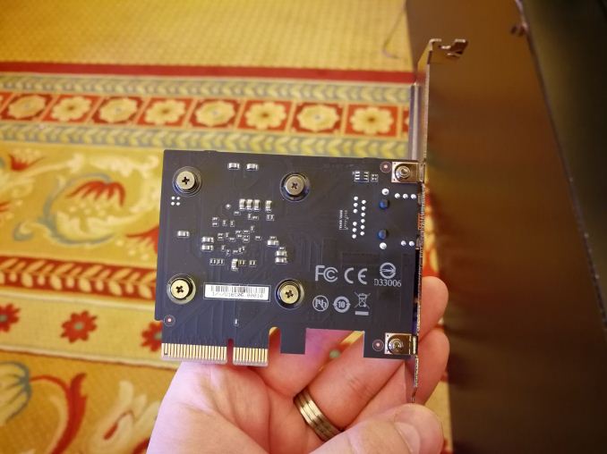
Anandtech: GIGABYTEs GC-AQC107 10G Ethernet PCIe Card Launched and Listed
GIGABYTE has added the GC-AQC107 10 GbE PCIe card it demonstrated early this year at CES to the list of products on its website. The product is also listed on both Amazon US and Amazon UK but is currently unavailable. When the network card is released, GIGABYTE will be the third company to offer a 10 GbE NIC based on an Aquantia chip.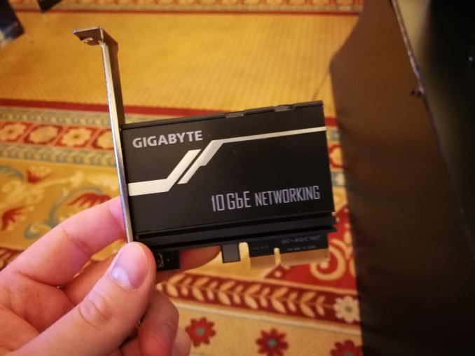
The GIGABYTE GC-AQC107, powered by the Aquantia AQtion AQC107 controller, supports 100M, 1G, 2.5G, 5G and 10G networking standards over CAT5e or CAT6/6a cables and RJ45 connectors (depending on the distance). The card resembles Aquantia’s reference design, so it is not considerably different from 10 GbE boards from Aquantia itself. To ensure that the AQC107 chip does not overheat, GIGABYTE equipped the GC-AQC107 with an aluminum heatsink. Furthermore, to make it easier for consumers to set up their networks, the RJ45 connector features LEDs monitoring data transmission. As for requirements, the GC-AQC107 can be installed into any modern PC that has a spare PCIe x4 slot and is running Microsoft Windows 7 and higher, as well as various Linux operating systems.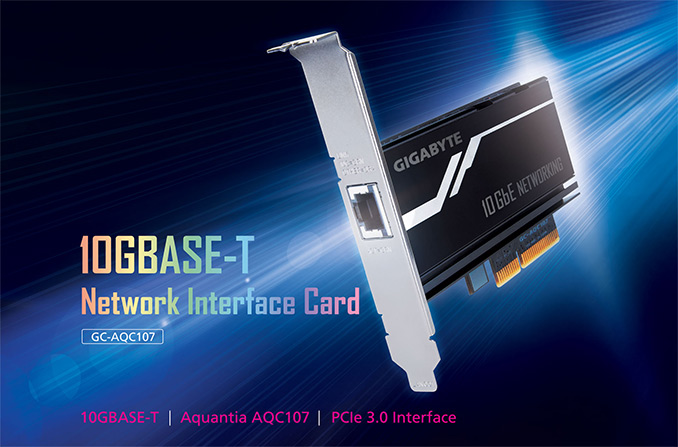
 The listing on the official website, as well as on Amazon, indicates that the GC-AQC107 will be available shortly. An important question surrounding the card is how much will it cost. Aquantia’s MSRP for its own AQN-107 card is $127, but ASUS charges $99 for its 10 GbE NIC based on the AQC107, so expect the GIGABYTE GC-AQC107 to cost between $99 and around $130.
GIGABYTE 10GBase-T Card for Consumers GC-AQC107 Controller Aquantia AQC-107 100BASE-T Yes 1000BASE-T Yes 2.5GBASE-T Yes 5GBASE-T Yes 10GBASE-T Yes (over Cat6 cables) Ports 1 Price unknown Release Date Q4 2017 Additional Information Link
Meanwhile, a quick check of leading U.S. retailers revealed that 10 GbE-supporting switches are still quite expensive and the most affordable one is the ASUS XG-U2008 10GBase-T that is available for $220 from Amazon and Newegg.
Gallery: GIGABYTEs GC-AQC107 10G Ethernet PCIe Card Launched and Listed


Buy GIGABYTE GC-AQC107 10 GbE NIC on Amazon.com
Related Reading- GIGABYTE Exhibits an Aquantia AQC107 based 10G Ethernet PCIe Card
- ASUS Launches XG-C100C 10 GBase-T Adapter: Aquantia AQC107, $99
- Lower Cost 10GBase-T Switches Coming: 4, 5 and 8-port Aquantia Solutions at ~$30/Port
- Aquantia Launches New 2.5G/5G Multi-Gigabit Network Controllers for PCs
- Aquantia Launch AQtion 5G/2.5G/1G Multi-Gigabit Ethernet Cards (NICs) for PCIe
- GIGABYTE Exhibits an Aquantia AQC107 based 10G Ethernet PCIe Card
- AKiTiO Displays Thunderbolt 3 to 10GBase-T Adapter
More...
-
11-09-17, 11:35 PM #7509
Anandtech: NVIDIA Announces Earnings of $2.6 Billion for Q3 2018, Once Again Sets Pro
This afternoon, NVIDIA announced its earnings for their 2018 fiscal year’s third quarter, which spans July 31 to October 29, 2017 (and not to be confused with the 2017 calendar year third quarter). Driven largely by sales of Pascal based gaming graphics cards and Volta based datacenter products, NVIDIA posted a record revenue of $2.636 billion, up 32% from a year ago. Gross margin increased by half a percent year-over-year to 59.5% as well. Similar to last quarter, the increase in revenue and gross margin were accompanied with an increase in operating income to $895 million, up 40% from Q3 2017. Overall, net income was reported at $838 million, up 55% year-over-year, with diluted earnings per share at a record $1.33, up 60% year-over-year.
Bringing it together, Q3 2018 is another record quarter for NVIDIA, fueled in part by the seasonally strongest quarter (July to September) for GPU shipments and the PC market as a whole.
As usual, NVIDIA’s gaming segment provides the lion’s share – around 59% – of the company’s Q3 revenue, riding on PC gaming. Up 25% year-over-year, gaming revenue was reported at $1.561 billion, a figure not to be taken lightly: NVIDIA’s Q3 2018 gaming segment alone earned around 95% of AMD’s total revenue of their positive Q3 2017. Put another way, NVIDIA’s gaming segment earned more than NVIDIA as a whole did back in August 2016 at the end of their Q2 2017. As all GeForce sales are counted in the gaming segment, this growth includes some waning cryptocurrency mining demand that spiked in the second calendar year quarter; as for crypto-specific boards, they are categorized into the OEM and IP segment.NVIDIA Q3 2018 Financial Results (GAAP) Q3'2018 Q2'2018 Q3'2017 Q/Q Y/Y Revenue $2636M $2230M $2004M +18% +32% Gross Margin 59.5% 58.4% 59.0% +1.1% +0.5% Operating Income $895M $688M $639M +30% +40% Net Income $838M $583M $542M +44% +55% EPS $1.33 $0.92 $0.83 +45% +60%
Officially, NVIDIA attributes the gaming revenue growth to continued sales of Pascal based gaming GPUs. While NVIDIA did launch the GTX 1070 Ti last week, with preorders opening in late October, this occurred at the very tail end of their fiscal quarter, and so related revenue would be seen in their Q4 fiscal report.
On the Quadro side of matters, NVIDIA’s professional visualization segment also saw an increase, up 15% year-over-year to $239 million, driven by high-end mobile platforms. While this segment has not grown by the same leaps-and-strides as gaming or datacenter, $239 million is still record quarterly revenue for NVIDIA’s very high margin professional visualization segment.NVIDIA Quarterly Revenue Comparison (GAAP)
($ in millions)In millions Q3'2018 Q2'2018 Q3'2017 Q/Q Y/Y Gaming $1561 $1186 $1244 +32% +25% Professional Visualization $239 $235 $207 +2.0% +15% Datacenter $501 $416 $240 +20% +109% Automotive $144 $142 $127 +1.0% +13% OEM & IP $191 $251 $186 -24% +3.0%
In light of NVIDIA’s continued AI and high-performance computing (HPC) efforts, shipping their first Volta-based DGX system in September, datacenter continues to be NVIDIA’s second largest market by revenue. Up 109% year-over-year, datacenter revenue was reported at a record $501 million, breaking the half-billion dollar mark. NVIDIA stated that the growth reflected shipments of Volta based GPUs, as well as increased hyperscale and cloud demand for deep learning training and GPU compute. Volta continues to ramp up, having started the previous quarter. Comparable to last quarter, this puts datacenter at just above 19% of their total revenue. Though still far from NVIDIA's gaming revenues, the datacenter business is at this point the darling of the company, as the massive growth potential for this market and its high margin outlook is what's been fueling NVIDIA's own growth for the past two years.
The OEM and IP segment reported the most modest gains, up 3% year-over-year and down 24% sequentially. The quarter-to-quarter sequential decrease is largely due to lessening mining demand, and NVIDIA commented that cryptomining boards accounted for $70 million in Q3 as opposed to $150 million in Q2.
Last, and for this quarter the least, automotive revenue was up 13% year-over-year to total at a record $144 million, primarily infotainment modules, but also including production DRIVE PX platforms and self-driving car development agreements. Along with revenue from Nintendo Switch SoC modules, this contributed to a 26% sequential and 74% year-over-year increase for Tegra revenue.
Taking a step back, the past two years have seen the gaming and datacenter segments act as the main drivers for this kind of quarterly growth. That being said, this fiscal year quarter has seen that rapid increase slow down compared to recent quarters.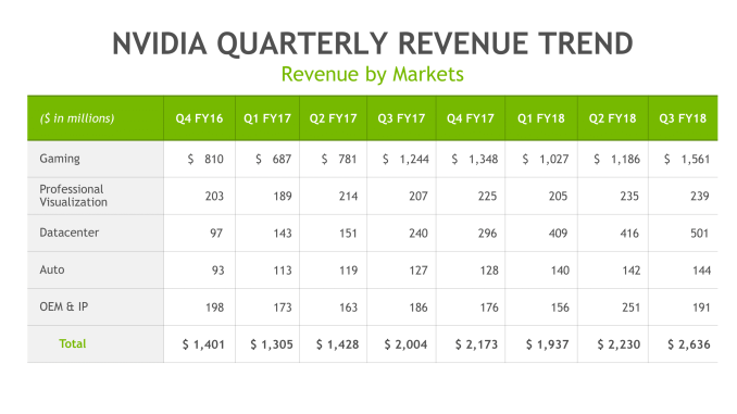
Q3 2018 also saw NVIDIA put $61 million to research and development, up around 72% sequentially and 57% year-to-year.
For Q4 2018, NVIDIA looks to set a record year in 2017, expecting total Q4 revenue between $2.59 and $2.70 billion, coupled with gross margins between 59.2% and 60.2%.
More...
-
11-10-17, 05:37 AM #7510
Anandtech: Qualcomm Launches 48-core Centriq for $1995: Arm Servers for Cloud Native
Following on from the SoC disclosure at Hot Chips, Qualcomm has this week announced the formal launch of its new Centriq 2400 family of Arm-based SoCs for cloud applications. The top processor is a 48-core, Arm v8-compliant design made using Samsung’s 10LPE FinFET process, with 18 billion transistors in a 398mm2 design. The cores are 64-bit only, and are grouped into duplexes – pairs of cores with a shared 512KB of L2 cache, and the top end design will also have 60 MB of L3 cache. The full design has 6 channels of DDR4 (Supporting up to 768 GB) with 32 PCIe Gen 3.0 lanes, support for Arm Trustzone, and all within a TDP of 120W and for $1995.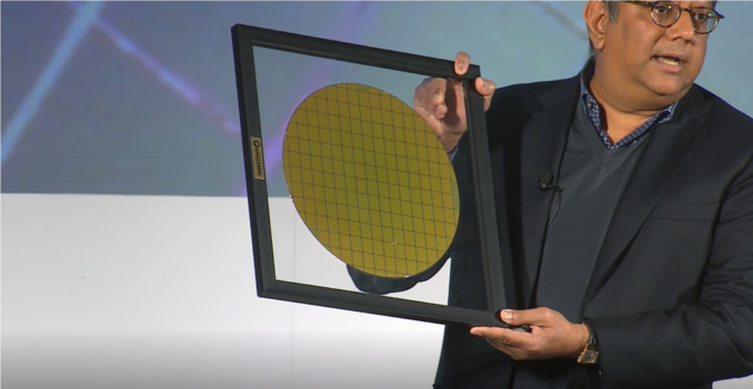
We covered the design of Centriq extensively in our Hot Chips overview, including the microarchitecture, security and new power features. What we didn’t know were the exact configurations, L3 cache sizes, and a few other minor details. One key metric that semiconductor professionals are interested in is the confirmation of using Samsung’s 10LPE process, which Qualcomm states gave them 18 billion transistors in a 398mm2 die (45.2MTr/mm2). This was compared to Intel’s Skylake XCC chip on 14nm (37.5MTr/mm2), but we should also add in Huawei’s Kirin 970 on TSMC 16FF (55MTr/mm2). Today Qualcomm is releasing all this information, along with a more detailed block diagram of the chip.
The chip has 24 duplexes, essentially grouped into sets of four. Connecting them all is a bi-directional segmented ring bus, with a mid-silicon bypass to speed up cross-core transfers. This ring bus is set with 250 GBps of aggregate bandwidth. Shown in the diagram are 12 segments of L3 cache, which means these are shipped with 5 MB each (although there may be more for yield redundancy). This gives a metric of 1.25 MB of L3 cache per core, and for the SKUs below 48 cores the cache is scaled accordingly. Qualcomm also integrates its inline memory bandwidth compression to enhance the workflow, and provides a cache quality of service model (as explained in our initial coverage). Each of the six memory controllers supports a channel of DDR4-2667, with support up to 768GB of memory and a peak aggregate bandwidth of 128 GB/s.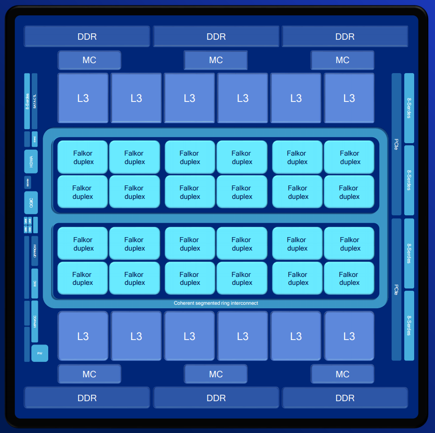
Starting with the chips on offer, Qualcomm will initially provide three different configurations, starting with 40 cores at 2.3 GHz (2.5 GHz turbo), up to 46 and 48 cores both at 2.2 GHz (2.6 GHz turbo). All three chips are somewhat equal, binned depending on active duplexes and cache, with $1995 set for the top SKU (other prices were not revealed). Qualcomm is aiming to attack current x86 cloud server markets on three metrics: performance per watt, overall performance, and cost. In that regard it offered three distinct comparisons, one for each chip:Qualcomm Centriq 2400 Series AnandTech.com Centriq 2460 Centriq 2452 Centriq 2434 Cores 48 46 40 Base Frequency 2.2 GHz 2.2 GHz 2.3 GHz Turbo Frequency 2.6 GHz 2.6 GHz 2.5 GHz L3 Cache 60.0 MB 57.5 MB 50 MB DDR4 6-Channel, DDR4-2667 PCIe 32 PCIe 3.0 TDP 120 W 120 W 110 W Price $1995 $1373 $888
- Centriq 2460 (48-core, 2.2-2.6 GHz, 120W) vs Xeon Platinum 8180 (28-core, 2.5-3.8 GHz, 205W)
- Centriq 2452 (46-core, 2.2-2.6 GHz, 120W) vs Xeon Gold 6152 (22-core, 2.1-3.7 GHz, 140W)
- Centriq 2434 (40-core, 2.3-2.5 GHz, 110W) vs Xeon Silver 4116 (12-core, 2.1-3.0 GHz, 85W)
Qualcomm provided some SPECint_rate2006 comparisons between the chips, showing Centriq either matching or winning in performance per thread, beating in performance per watt, and up to 4x in performance per dollar. It should be noted that the data for the Intel chips were interpolated from other Xeon chips.
One interesting bit of data from the launch was the power consumption results provided. As a server or cloud CPU scales to more cores, there will undoubtedly be situations where not all the cores are always drawing power, either due to how the algorithm works or the system is waiting on data. Normally the TDP values are given as a measure of power consumption, despite the actual definition of thermal dissipation requirements – a 120W chip does not always draw 120W, in other words. To this end, Qualcomm provided the average power consumption of the 120W Centriq 2460 while running SPECint_rate2006.
It shows a median power consumption of 65W, peaking just below 100W for hmmer and h264ref. The other interesting point is the 8W idle power, which is indicated as for only when C1 is enabled. With all idle states enabled, Qualcomm claims under 4W for the full SoC. Qualcomm was keen to point out that this includes the IO on the SoC, which requires a separate chipset on an Intel platform.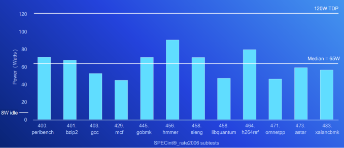
Any time an Arm chip comes into the enterprise space, thoughts immediately turn to high-performance, and Qualcomm is keen here to point out that while performant, their main goal is to cloud services and hyper-scale, such as scale-out situations, micro-services, containers, and instance-based implementations. At the launch in San Diego, they rolled out quotes from Alibaba, Google, HPE, and Microsoft, all of whom are working closely with Qualcomm for deployment. Demonstrations at the launch event included NoSQL, cloud automation, data analytics with Apache Spark, deep learning, network virtualization, video and image processing, compute-based bioinformatics, OpenStack, and neural networks.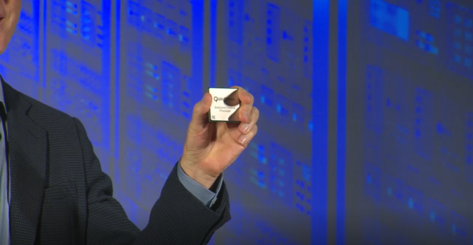
On the software side, Qualcomm is working with a variety of partners to enable and optimize their software stacks for the Falkor design. At Hot Chips, Qualcomm also stated that there are plans in the works to support Windows Server, based on work done with their Snapdragon on Arm initiative, although this seemed to be missing from the presentation.
Also as a teaser, Qualcomm gave the name of its next-generation enterprise processor. The next design will be called the Qualcomm Firetail, using Saphira cores. (Qualcomm has already trademarked both of those names).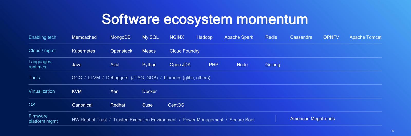
Qualcomm Centriq is now shipping (for revenue) to key customers. We should be on the list for review samples when they become available.
Related Reading
Gallery: Qualcomm Launches 48-core Centriq for $2000: Arm Servers for Cloud Native Applications


More...


 Quote
QuoteThread Information
Users Browsing this Thread
There are currently 6 users browsing this thread. (0 members and 6 guests)


Bookmarks