

Results 7,651 to 7,660 of 12096
Thread: Anandtech News
-
12-19-17, 07:27 AM #7651
Anandtech: The Crucial MX500 1TB SSD Review: Breaking The SATA Mold
The Crucial MX500 is the next generation SATA SSD from Micron's consumer division. As the latest MX series drive, the MX500 is positioned to be a mainstream product with solid performance but without much of a premium over entry-level SSDs. Since Micron has not yet released a consumer NVMe SSD, the Crucial MX500 will also serve as their flagship consumer drive and the showcase for their new 64-layer 3D NAND flash memory.
Micron is one of several NAND flash manufacturers to introduce 64L 3D NAND this year. They're a bit late to the party considering that their NAND manufacturing partner Intel introduced started shipping their 64L 3D TLC in a retail drive six months ago, but Micron hasn't missed their chance. All of the major NAND flash manufacturers except SK Hynix are still in the early phases of rolling out their 64L 3D NAND. In a major change from the state of the industry for the past several years, there's no clear leader: Intel and Micron, Toshiba and Western Digital/SanDisk, and Samsung are all putting out products with competitive performance and pricing. The market is up for grabs, and the SATA segment that still makes up the bulk of consumer SSD sales is where the competition is fiercest.
To prepare for this next round of competition, the Crucial MX500 brings major hardware changes to what has been a slowly evolving product line stretching back to the first 6Gbps SATA SSD.
More...
-
12-19-17, 07:27 AM #7652
Anandtech: Intel Lists Knights Mill Xeon Phi on ARK: Up to 72 cores at 320W with QFMA
Today it was noticed, without any fanfare from Intel, that Knights Mill information has been uploaded to Intel’s specification database ARK. There are three known SKUs so far, with up to 72 cores and a 320W TDP. The Xeon Phi 'Knights Mill' products are a new iteration on the older 'Knights Landing' family, with a silicon change for additional AVX-512 instructions. As far as we can tell, these parts will only be available as socketable hosts and not as PCIe add-in cards.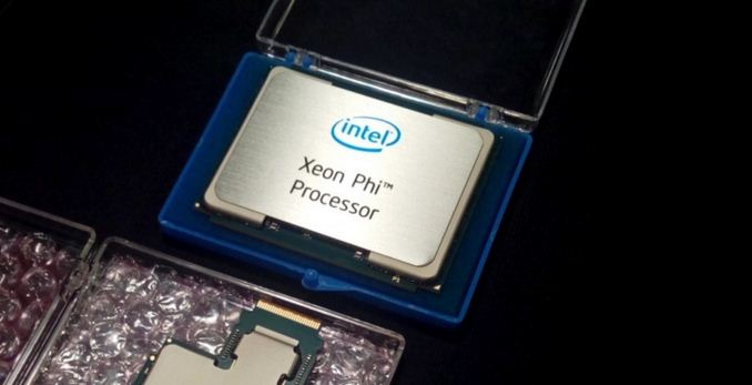
More...
-
12-19-17, 02:13 PM #7653
Anandtech: Corsair Launches the Neutron NX500 1.6 TB PCIe SSD
Corsair has started selling its highest-capacity PCIe SSD to date, the Neutron NX500, featuring 1.6 TB of NAND. The drive is based on the Phison E7 controller as well as Toshiba’s MLC NAND, so it is going to appeal to those seeking for a proven MLC-based storage solution with loads of flash memory reserved for over-provisioning and a five-year warranty. It should be noted however that with big capacity comes a big cost.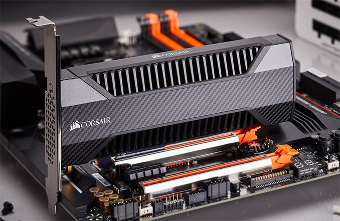
The new Neutron NX500 1.6 TB is an HHHL card, just like the versions with 400 GB and 800 GB of usable memory. From an architecture point of view, the Corsair Neutron NX500 SSDs are similar to the Force MP500 drives launched this time last year: they are powered by the Phison PS5007-E7 controller, use Toshiba’s MLC NAND memory made using a 15 nm fabrication process, and have a PCIe 3.0 x4 interface. The general feature set of the E7 controller is also well known: it has four compute cores with eight NAND channels, supports error correction with 120-bit/2KB BCH code (that is good enough for planar MLC NAND), the NVMe 1.1b protocol with the NVMe L1.2 power saving mode, end-to-end data path protection, advanced global wear-leveling and so on.
Gallery: Corsair Neutron NX500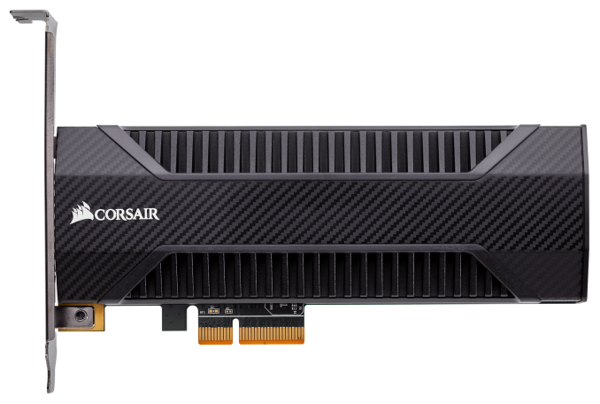


When it comes to performance, everything is by the numbers: the drives are rated for a sequential read speed of up to 3000 MB/s, and a sequential write performance of up to 2400 MB/s. Because the Neutron NX500 SSDs use Phison’s latest firmware, they can perform up to 300K random read IOPS (input/output operations per second) as well as 270K random write IOPS, which is considerably higher than the random performance of the MP500 and some other E7-powered products.
The key features that differ the Neutron NX500 from the vast majority of drives featuring the Phison PS5007-E7 controller are the add-in-card form-factor as well as usage of large amounts of NAND flash for overprovisioning to guarantee long-term reliability and performance. The Neutron NX500 carry 512 GB, 1 TB and 2 TB of raw NAND flash memory, but users can access 400 GB, 800 GB and 1.6 TB of NAND, depending on the model. With massive amounts of memory used for overprovisioning. Corsair offers them with a five-year warranty, which is not that common these days, compared to the 1-3 years given with most M.2 drives.
The huge amount of MLC NAND for overprovisioning has a knock-on effect on the pricing of the Corsair Neutron NX500 drives. The configurations featuring 400 GB and 800 GB of NAND flash memory were launched earlier this year at $319.99 and $659.99 in the U.S., respectively. The 1.6 TB configuration became available at Corsair’s online store this week at $1575 in the US, €1770 in the EU, and £1615 in the UK.
If the form-factor and overprovisioning are clear advantages of the Neutron NX500 1.6 TB, then its high price point (conditioned by MLC NAND) is its main drawback. The final cost of ~$1 per end-user visible gigabyte is rather high for a consumer SSD in late 2017. Corsair’s product is available for $1633 at Amazon, a bit cheaper than Samsung charges for its 960 PRO 2 TB drive ($1641), but with obviously less immediate capacity.
On paper, the Samsung 960 Pro is faster than the Neutron NX500, which makes the former not only cheaper on a per-GB basis, but also more preferable for general use. However, the Neutron NX500 is rated for 2793 TBW, whereas the Samsung 960 Pro 2 TB is rated for 1200 TBW. Typically, SSD makers set rather conservative TBW targets different from the real world endurance, but if one only considers “official” TBW ratings, then this is where the Neutron NX500 1.6 TB excels the Samsung 960 Pro 2 TB.
Corsair Neutron NX500 Series Specifications CSSD-N400GBNX500 CSSD-N800GBNX500 CSSD-N1600GBNX500 Capacities 400 GB 800 GB 1600 GB Form Factor HHHL Interface PCIe 3.0 x4 (NVMe 1.2) Controller Phison PS5007-E7 NAND Toshiba's 128 Gb MLC
15 nm process technologyDRAM 512 MB unknown unknown Sequential Read up to 3000 MB/s Sequential Write up to 2400 MB/s up to 2300 MB/s Random-R (4 KB) IOPS up to 300K Random-W (4 KB) IOPS up to 270K Power DEVSLP 500 mW (listed, perhaps wrong?) Operating 5 ~ 7 W (?) Endurance 698 TBW 698 TBW 2793 TBW Warranty Five years Price $320 $660 $1575 Related Reading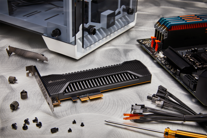
- The Corsair Neutron NX500 (400GB) PCIe SSD Review: Big Card, Big Pricetag
- Corsair Releases Force MP500 SSDs: 3 GB/s, Phison PS5007-E7, MLC NAND
- The Patriot Hellfire M.2 480GB Review: Phison NVMe Tested
- PNY Launches CS2030 SSDs: Phison PS5007-E7, MLC NAND, 2.8 GB/s
- The Samsung 960 Pro (2TB) SSD Review
More...
-
12-19-17, 04:14 PM #7654
Anandtech: More Ryzen Mobile: Acer Swift 3 with 2700U and 2500U Listed, From $750
Back at the Ryzen Mobile launch, AMD announced three primary partners with three devices: the HP Envy x360, the Acer Swift 3, and the Lenovo Ideapad 720S. At the time, only HP had some information available, and has since pushed the Envy x360 to retail. The other two have been surprisingly quiet about their models, but today Acer steps up to the plate with lists and pricing.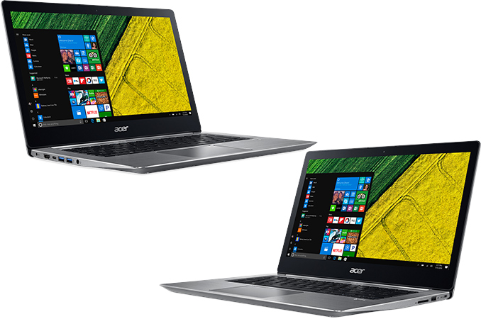
Acer has, without any fanfare, added two laptops powered by AMD’s Ryzen Mobile 2500U and Ryzen Mobile 2700U processors to its product lineup. The laptops have a metallic chassis, with a 15.6” IPS panel featuring a 1920x1080 resolution. Inside are AMD’s 15 W Ryzen Mobile APUs, the Ryzen 5 2500U and the Ryzen 7 2700U, each with four cores, eight threads, and Vega 8 (512SPs) or Vega 10 (640SPs) integrated graphics respectively.
The new systems have 8 GB of DDR4 memory, and storage comes in at either a 256 GB SSD or a 512 GB SSD (no word if SATA or PCIe). For connectivity, the AMD-powered Swift 3 uses an 802.11ac Wi-Fi + Bluetooth module, three USB Type-A ports, one USB Type-C header, and an HDMI output. Finally, the notebooks are equipped with a backlit keyboard, a webcam, two speakers and a microphone. The Acer Swift 3 design is one of a typical workhorse notebook, for consumers who demand to have decent performance and portability but do not necessarily need a portable workstation or an ultrabook. Interestingly the specification sheets say that the battery is listed as 3340 mAh, which at 17.4 volts makes around 58 Wh, although the voltage of the battery is not specified.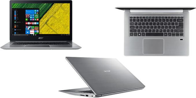
Back at the Ryzen Mobile launch, AMD stated that the chassis for the Swift 3 was designed to dissipate 25W at maximum, so by putting a 15W APU in there, it allows for a higher XFR boost frequency, as well as boosting for longer. The launch article also listed the DRAM being in dual channel operation, up to DDR4-2133. Acer confirms neither of these points, but dual-channel would be a good choke point to alleviate for the graphics - the DDR4-2133 is below the DDR4-2400 that the Ryzen APU platform supports, however.
By today’s standards, the Ryzen Mobile-based Swift 3 units can hardly be called thin or light — the device weighs around 2.2 kilograms and is 1.87 cm thick. Acer could have lower the weight by choosing plastic over metal for the chassis, but at the cost of rigidity, look and overall user experience. Meanwhile, being ultraportable is not the purpose of the vast majority of 15.6” laptops anyway. To Acer’s credit, it’s worth pointing out that the Ryzen Mobile-based Swift 3 are slightly thinner (but a bit heavier) than HP’s Envy x360 featuring the same APUs. We currently have the Intel-based Swift 3 units in for testing, so this would be an interesting counterpoint.
Acer’s Swift 3 SF315-4-series notebooks are already listed on the company’s website, so expect them to be available commercially in the coming weeks. As for pricing, Acer's Taiwan site had the Swift 3 featuring the Ryzen Mobile 2500U and a 256 GB SSD listed at $750, whereas the more advanced Swift 3 featuring the Ryzen Mobile 2700U and a 512 GB drive was listed for $950 at retail.Acer Swift 3 Laptops Based on AMD Ryzen Mobile APUs SF315-41-R8PP
NX.GV7AA.003SF315-41-R6J9
NX.GV7AA.004Display Diagonal 15.6" Resolution 1920×1080 Type IPS CPU AMD Ryzen 5 2500U
4 Cores with SMT (8T)
2.0 GHz Base
3.8 GHz Turbo
mXFR Support
2 MB L2 + 4 MB L3
Vega 8 iGPU
15 WAMD Ryzen 7 2700U
4 Cores with SMT (8T)
2.2 GHz Base
3.8 GHz Turbo
mXFR Support
2 MB L2 + 4 MB L3
Vega 10 iGPU
15 WGraphics AMD Vega 8
512 stream processors
1100 MHzAMD Vega 10
640 stream processors
1300MHzRAM Capacity 8 GB Type DDR4 (frequency unknown) Storage 256 GB SSD 512 GB SSD Wi-Fi 802.11ac Wi-Fi module (unknown vendor) Bluetooth 4.x USB 2 × USB 3.0 Type-A
1 × USB 2.0 Type-A
1 × USB 3.0 Type-COther I/O HDMI 2.0a, webcam, TRRS connector for audio, speakers, microphone, SD card reader Dimensions Height 18.8 mm | 0.74" Width 370.5 mm | 14.59" Depth 255 mm | 10.04" Weight 2.2 kg | 4.85 lb Battery Capacity 3320 mAh (58 Wh at 17.4V?) Price $750 $950
Related Reading- Ryzen Mobile is Launched: AMD APUs for Laptops, with Vega and Updated Zen
- Ryzen Mobile Now On Sale: HP’s ENVY X360
- HP Announces ENVY x360 15 With Ryzen Mobile
- AMD Makes a Surprise Appearance: Ryzen Mobile with Qualcomm LTE
Gallery: Acer Adds Ryzen Mobile-Based Swift 3 Laptops to Lineup: 15.6-inch, Quad-Core, Starts at $750

More...
-
12-20-17, 10:19 AM #7655
Anandtech: Samsung Starts Production of 8 Gb DDR4-3600 ICs Using 2nd Gen 10nm-Class T
Samsung late on Wednesday said that it had initiated mass production of DDR4 memory chips using its second generation '10 nm-class' fabrication process. The new manufacturing technology shrinks die size of the new DRAM chips and improves their performance as well as energy efficiency. To do that, the process uses new circuit designs featuring air spacers (for the first time in DRAM industry). The new DRAM ICs (integrated circuits) can operate at 3600 Mbit/s per pin data rate (DDR4-3600) at standard DDR4 voltages and have been validated with major CPU manufacturers already.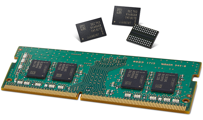
As it usually happens with Samsung’s major DRAM-related announcements, the news today consists of two parts: the first one is about the new DDR4 IC itself, the second part is about the second generation '10 nm-class' (which Samsung calls '1y' nm) manufacturing technology that will be used for other DRAM products by the company. Both parts are important, but let’s start with the new chip.
Samsung’s new DDR4 chip produced using the company’s 1y nm fabrication process has an 8-gigabit capacity and supports 3600 MT/s data transfer rate at 1.2 V. The new DRAM runs 12.5% faster than its direct predecessor (known as Samsung C-die, rated for 3200 MT/s) and is claimed to be up to 15% more energy efficient as well. In addition, the latest 8Gb DDR4 ICs use a new in-cell data sensing system that offers a more accurate determination of the data stored in each cell and which helps to increase the level of integration (i.e., make cells smaller) and therefore shrink die size.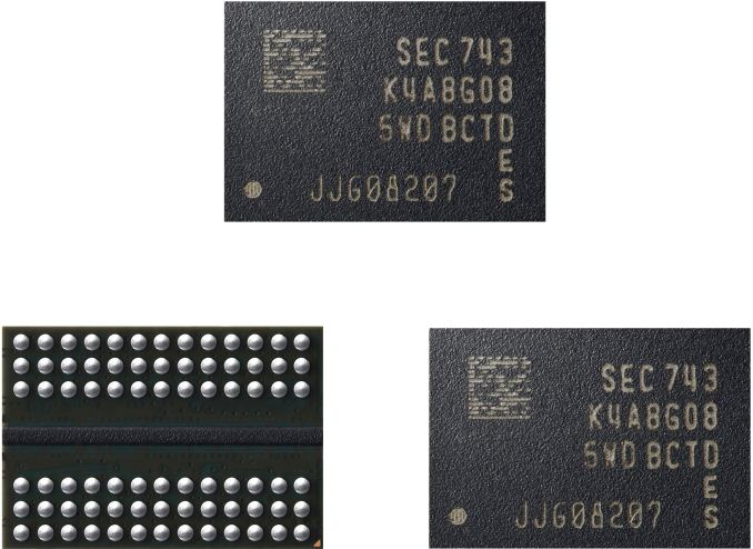
Samsung says that the new 8Gb DDR4 chips feature an “approximate 30% productivity gain" when compared to similar chips made using the 1x nm manufacturing tech. Samsung has not clarified what is meant "productivity gain", but is likely to refer to the function of DRAM bit output per wafer and wafer cycle time (yet, at a deeper level it could include other metrics that take into account energy consumption, headcount, etc.). Since wafer cycle time is a figure that rarely gets published, the key takeaway from the announcement is that the 1y nm technology and the new in-cell data sensing system enable Samsung to shrink die size and fit more DRAM dies on a single 300-mm wafer. Meanwhile, the overall 30% productivity gain results in lower per-die costs at the same yield (this does not mean that the costs are 30% lower though) and increases DRAM bit output.
Samsung does not release exact smallest hhalf-pitchsize of the new DRAMs (the feature size used to give names to DRAM process technologies), so at this point we do not know any details about the new chip’s geometries. Given that we are dealing with a 1y process, it logical to assume that the smallest half pitch size is from 14nm to 16 nm, but this is a speculation at this point. What we do know is that Samsung’s 1y nm process technology continues to use ArF (argon fluoride) immersion lithography tools presumably with quadruple patterning (so no EUV). Meanwhile, to reduce parasitic capacitance, Samsung placed air spacer around its bit lines, which helps to increase DRAM performance.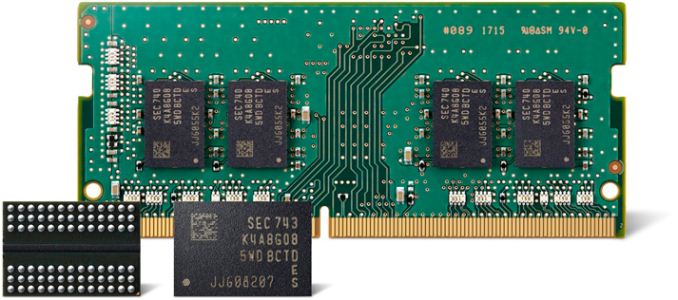
Speaking of performance, it is noteworthy that Samsung’s C-die DRAMs have not been used by companies like Corsair and G.Skill for their leading-edge memory modules for enthusiasts. Apparently, both companies still use the time-proven Samsung B-die ICs made using 20 nm process technology. It remains to be seen whether the aforementioned manufacturers jump to the new 1y nm 8 Gb DDR4 ICs and when.
Samsung says that the new in-cell data sensing system as well as air spacers will be used to make other types of DRAM, including DDR5, HBM3, LPDDR5, and GDDR6 — meaning that these two elements will be used for years to come. Of course, it will be a while before the first three standards enter commercial production, but GDDR6 with the aforementioned enhancements could be produced in the foreseeable future and using the 1y nm process.
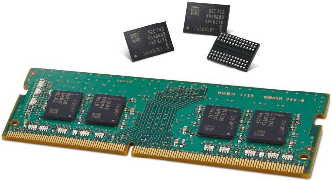
CPU developers (likely Intel, AMD, IBM, Qualcomm, etc.) have already validated the new 8 Gb DDR4-3600 memory chips produced using Samsung’s 2nd generation 10 nm-class process technology. The next step for Samsung is to validate memory modules with PC makers and put these modules into the next-gen systems. It is noteworthy that this time Samsung only displays the new 8 Gb ICs on an SO-DIMM, but not on a desktop-class memory module. It is unknown whether this has something to do with product positioning and/or Samsung's own plans for modules (e.g., laptops are addressed first), but previously Samsung always published pictures of its latest DRAMs both on DIMMs and SO-DIMMs.
Along with the announcement of the new 8 Gb DDR4 DRAM IC, Samsung also said that it would ramp up production of memory (not only DDR4, but also mobile DRAM, etc.) using both of its 10 nm-class fabrication processes to meet “growing demand for DRAM in premium electronic systems worldwide”.
Related Reading- Samsung Begins To Produce DDR4 Memory Using '10nm Class' Process Tech
- Samsung Pre-Announces 16 Gbps GDDR6 Chips for Next-Gen Graphics Cards
- Samsung Starts Production of 512 GB UFS NAND Flash Memory: 64-Layer V-NAND, 860 MB/s Reads
- Samsung Starts Mass Production of Chips Using 10nm Low Power Plus (10LPP) Process Tech
- Samsung’s 8LPP Process Technology Qualified, Ready for Production
- Samsung Details 11LPP Process Technology: 10 nm BEOL Meets 14 nm Elements
More...
-
12-20-17, 10:19 AM #7656
Anandtech: Khronos Group Launches the Neural Network Exchange Format
Today the Khronos Group, the industry consortium behind OpenGL and Vulkan, released a v1.0 provisional specification for its Neural Network Exchange Format (NNEF). First announced last year, this provisional stage is aimed at getting industry feedback on real-world use. While its name encapsulates its purpose, more specifically NNEF will act as a compatible format that can transfer trained neural networks between frameworks or to a wide range of inferencing hardware. Khronos is hoping that NNEF will act as a common format for all the myriad frameworks, such as Caffe, TensorFlow, Theano, and Torch, and be as ubiquitous in neural network porting in the same way PDFs are used for documents.
Much of the strength of NNEF comes from its bifurcated file structure, where there is a general and compatible flat level along with a complicated and optimizable compositional level. NNEF has also been designed with the understanding that deep learning is still a young and rapidly advancing field, where certain AI or neural network methods or framework types may become quickly displaced.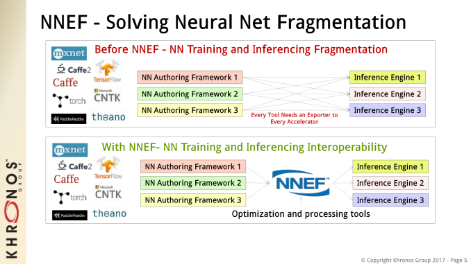
NNEF will also complement Khronos’ OpenVX, a high-level graph-based API intended for cross-platform use in computer vision, and both working groups have already been collaborating. The upcoming releases of OpenVX will feature a NNEF Import extension, which would provide more flexibility to the format. As a specification, NNEF does not include tools, and Khronos is pursuing an open source strategy, with current projects on an NNEF syntax parser/validator and exporters for specific frameworks.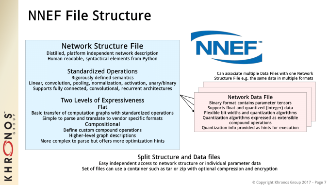
This approach contrasts with the similar Open Neural Network Exchange (ONNX) started by Facebook and Microsoft, where the format specification is essentially part of the open source project. NNEF itself is a standardized specification, with open source projects complementing it.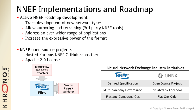
Overall, Khronos identifies two general use-cases for NNEF: for using a given trained network with a given inferencing engine, and for transposing a trained network from one framework to another. The former has been the focus and NNEF is being developed with silicon vendors in mind. A static standardized specification is particularly useful for hardware manufacturers, and NNEF’s two-level data topology allows silicon designers to optimize for their specific hardware via the custom compound operations capability.
On that note, this launch of the provisional specification is not limited to manufacturers, and Khronos is looking for the industry feedback to refine their specification and its strongest use-cases for a final release. Khronos has noted that framework-to-framework transposition might be one of several avenues that researchers could explore on their own as part of the open source projects.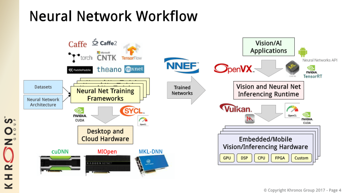
While NNEF has no set date to be finalized, Khronos mentioned that a 3 to 6 month period before finalization would be typical.
More project details can be found on the NNEF GitHub repository.
Gallery: Khronos Group NNEF 1.0 Provisional Slide Deck


Source: Khronos Group
Related Reading- The Khronos Group Announces New Standards Collaboration for VR Integration
- GTC Europe Live Blog: How to Get Regulatory Approval for an AI-based Autonomous Car
More...
-
12-20-17, 12:46 PM #7657
Anandtech: The NVIDIA Titan V Preview - Titanomachy: War of the Titans
Today we're taking a preview look at NVIDIA's new compute accelerator and video card, the $3000 NVIDIA Titan V. In Greek mythology Titanomachy was the war of the Titans, and for our first look at the Titan V we’re staging our own version of Titanomachy. We’ve rounded up all four of the major Titans, from the OG GTX Titan to the new Titan V, and have tested them on a cross-section of compute, gaming, and professional visualization tasks in order to see what makes the Titan V tick and how the first graphics-enabled Volta card fares.
Today’s preview is just that, a preview – we have even more benchmarks cooking in the background, including some cool deep learning stuff that didn’t make the cut for today’s article. But for now we have enough data pulled together to see how NVIDIA’s newest Titan compares to its siblings, and why the Volta architecture just may be every bit as big of a deal as NVIDIA has been making of it.
More...
-
12-21-17, 08:11 AM #7658
Anandtech: The Microsoft Surface Book 2 (15-Inch) Review: Second Time's The Charm
We finally have the successor. After a troubled launch in late 2015 of the original Surface Book, Microsoft seemed to drag their feet when it came to updating what was one of the most interesting notebooks released in the last couple of years. The original Surface Book launched with some serious power management concerns, which were eventually sorted out, but then the company just left the model relatively untouched, except for a mid-generation update with a stronger GPU.
The wait is over though. Microsoft has released the Surface Book 2 as a worthy successor to the original, with many improvements. With the launch of the Surface Laptop earlier this year, which targets the $1000 price point, Microsoft was free to ratchet the Surface Book 2 up in performance, and price, and they’ve doubled the number of models, with both a 13.5-inch version, being the upgrade from the original, and a new 15-inch model which clearly targets the performance-starved users. For this review, Microsoft sent us the larger 15-inch model.
More...
-
12-21-17, 08:11 AM #7659
Anandtech: Apple Confirms CPU Limitation In Ageing Devices
Over the last week there's been increasing discussion and evidence of Apple's supposed introduction of CPU throttling mechanisms directly related to the battery wear level on Apple iPhones. The story started out with a report on Reddit of a user experiencing slow performance on an iPhone 6S and subsequent discovery that the performance restored to its full potential after a battery replacement.
The report prompted GeekBench author John Poole to make use of the GeekBench benchmark submission database to plot performance of individual devices against iOS versions and discover a clear trend of ever increasing distribution towards lower performance points with newer OS versions.
Matthew Panzarino from TechCrunch was able to get an official statement from Apple when enquiring about the problem:
Our goal is to deliver the best experience for customers, which includes overall performance and prolonging the life of their devices. Lithium-ion batteries become less capable of supplying peak current demands when in cold conditions, have a low battery charge or as they age over time, which can result in the device unexpectedly shutting down to protect its electronic components.Apple’s official statement sheds some light into the issue but comes short of an actual technical explanation of why the power management is failing. The company claims that the issue at heart is because of the battery degradation and its inability to supply sufficient current at a stable voltage.
Last year we released a feature for iPhone 6, iPhone 6s and iPhone SE to smooth out the instantaneous peaks only when needed to prevent the device from unexpectedly shutting down during these conditions. We’ve now extended that feature to iPhone 7 with iOS 11.2, and plan to add support for other products in the future.
Capacity and supply voltage of a battery decreases over time as a function of charge cycles and charging behaviour (Higher charging currents causing more degradation per cycle). This causes the total useable battery capacity before the cut-off voltage to decrease.
The problem facing the iPhones as Apple explains it is however two-fold; the issue at hand happens only during load spikes in which the battery isn’t able to maintain a high enough voltage for the PMIC to reliably be able to use as a source.
SoC blocks such as CPUs and GPUs can have very short transitions from idle to load causing steep transients and load spikes going above the +10W ranges. As batteries degrade over time and the cell impedance also rises also in function of the state of charge and temperature, the current flow becomes restricted and the cell is no longer able to satisfy the power requirement at a high enough operating voltage.
Apple’s approach to the issue is to limit the peak power spikes by reducing the CPU frequencies over time as a function of battery wear. This solution however raises several questions; how does Apple decide the throttling behaviour and was the core fault an engineering fault or design choice?
As demonstrated in John Poole’s dataset Apple is throttling the CPU frequency in several stages. What exactly defines the thresholds to reach these stages can be either a rather simplistic counter taking into account the charge cycles of a given battery, or (and more hopefully) a more dynamic method that would be able to take advantage of the battery PMIC’s capabilities of determining battery wear. Given however that it seems that the OS is limiting performance even at high state of charges, such as fully charges batteries, it seems that the limitation implementation is unfortunately of the more simplistic type.
The second question comes to regard to as why it came to the issue in the first place as this should be a universal issue affecting a greater number of smartphones, not just Apple iPhones.
The first unique characteristic separating Apple iPhones from other smartphones is that Apple is using a custom CPU architecture that differs a lot from those of other vendors. It’s plausible that the architecture is able to power down and power up in a much more aggressive fashion compared to other designs and as such has stricter power regulation demands. If this is the case then another question rises is if this is indeed just a transient load issue why the power delivery system was not designed sufficiently robust enough to cope with such loads at more advanced levels of battery wear? While cold temperature and advanced battery wear are understandable conditions under which a device might not be able to sustain its normal operating conditions, the state of charge of a battery under otherwise normal conditions should be taken into account during the design of a device (Battery, SoC, PMIC, decoupling capacitors) and its operating tolerances.
If the assumptions above hold true then logically the issue would also be more prevalent in the smaller iPhone as opposed to the iPhone Plus models as the latter’s larger battery capacity would allow for greater discharge rates at a given stable voltage. This explanation might also be one of many factors as to why flagship Android and other devices don’t seem to exhibit this issue, as they come with much larger battery cells.
While much of the latter part of this piece is just my personal conjecture as to the deeper causes of the problem, it is clear that this is a larger issue for Apple that has no simple solution (beyond replacing the battery). How this affects more recent devices such as the iPhone 8 and iPhone X, or verifying if indeed the Plus variants would be less prone to the problem is something that will require a lot of testing, collaboration and data collection over longer periods of time.
More...
-
12-21-17, 01:15 PM #7660
Anandtech: Keeping it Quick: G.Skill Launches a 32 GB Quad-Channel DDR4-4000 SO-DIMM
ASRock’s X299E-ITX/ac is the only Mini-ITX motherboard for Intel’s latest Core i7/Core i9 processors, and also the only consumer motherboard that requires enthusiast-class quad-channel SO-DIMM kits. The appeal of mini-ITX if for a niche, and going for 18-core support is another niche, but it looks like it has managed to create quite a market around itself. In the past couple of months, Corsair and G.Skill have been striving to offer the fastest memory for this mainboard, as well as supported notebooks and other DDR4 systems. Last week Corsair introduced its 32 GB DDR4-4000 CL19 kit and this week G.Skill followed up with its 32 GB DDR4-4000 solution with a bit lower latencies.
The G.Skill Ripjaws 32 GB quad-channel DDR4-4000 SO-DIMM kit consists of four 8 GB modules built upon pre-binned Samsung’s time-proven B-die 8 Gb DDR4 DRAM chips. The modules are designed to operate with CL18 18-18-38 latencies at 1.35 V, which is a bit lower when compared to Corsair’s DDR4-4000 SO-DIMMs that are speced for CL19 23-23-45 latencies at 1.35 V. G.Skill’s new modules are validated to work only on ASRock’s X299E-ITX/ac motherboard and their XMP 2.0 profiles in SPD are tailored for Intel’s Core i7/Core i9 (Skylake-X) processors.
Hitting DDR4-4000 is an important psychological milestone for enthusiast-class SO-DIMMs in general. From a pure technology point of view, Corsair’s and G.Skill’s high-end DDR4 kits bring the ASRock’s X299E-ITX/ac platform closer to fully-fledged HEDTs that use full-sized DDR4, at least when it comes to memory bandwidth. G.Skill’s fastest quad-channel kit for Intel’s Skylake-X processors is rated for DDR4-4200 with CL19 latency at 1.4 V, so performance gap between “baby” and “large” HEDTs is almost negligible (128 GB/s vs. 134.4 GB/s).G.Skill's Ripjaws DDR4 SO-DIMM Kits for SFF PCs Speed Sub-Timings Voltage Kit
Config.Kit
CapacityDDR4-3200 CL16 16-16-36 1.35 V 4×8 GB 32 GB 4×16 GB 64 GB DDR4-3600 4×8 GB 32 GB DDR4-3800 CL18 18-18-38 4×8 GB DDR4-4000 4×8 GB
For some reason, G.Skill decided not to cherry-pick SO-DIMM modules that can run at DDR4-4200 CL19, but went with DDR4-4000 CL18. It will be very interesting to see whether minor difference in latency will have any tangible effect on real-world performance of G.Skill’s kit when compared to Corsair’s kit, but the competition between two companies is definitely here.
G.Skill said that its Ripjaws 32 GB quad-channel DDR4-4000 CL18 kit will be available from its partners in Q1 2018. The company traditionally does not disclose MSRPs in its press releases because of DRAM pricing volatility, but given the exclusive nature of the product, it is going to be priced accordingly. Meanwhile, since there is a rival for the kit, we may expect competition to lower pricing of these products a bit. Having just reviewed the ASRock board, it might be time to get both kits in and have a shoot-out.
Buy ASRock X299E-ITX/ac on Amazon.com
Related Reading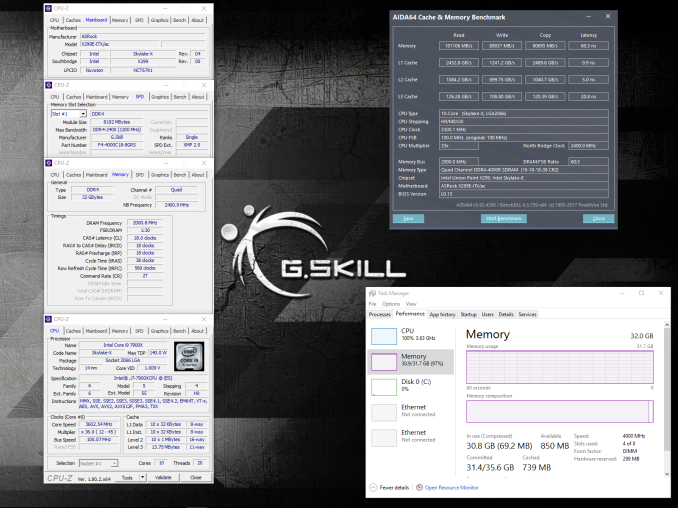
- Corsair Launches Vengeance 32 GB Quad-Channel DDR4-4000 SO-DIMM Kit for $595
- G.Skill Announces DDR4 SO-DIMM Kits up to DDR4-3800: Ripjaws for SFF
- G.Skill Announces Quad-Channel DDR4-4200 Kit for Intel Skylake-X CPUs
- ASRock’s X299E-ITX/ac Motherboard Now Available: Up to 18 Cores in Mini-ITX
- DRAM and Motherboard Makers Demonstrate Quad-Channel DDR4-4000+ Operation
- The Intel Skylake-X Review: Core i9 7900X, i7 7820X and i7 7800X Tested
- The Intel Core i9-7980XE and Core i9-7960X CPU Review Part 1: Workstation
- Transcend Introduces Extreme Temperature DDR4 SO-DIMMs
- Patriot to Release Viper DDR4-2400, DDR4-2800 SO-DIMMs for Laptops
More...


 Quote
Quote

Thread Information
Users Browsing this Thread
There are currently 8 users browsing this thread. (0 members and 8 guests)


Bookmarks