

Results 7,801 to 7,810 of 12096
Thread: Anandtech News
-
01-25-18, 11:41 AM #7801
Anandtech: Samsung Updates on GDDR6 Portfolio: 8 Gb and 16 Gb at Multiple Speeds
Samsung has issued an update to the GDDR6 announcement earlier this month. The company’s GDDR6 lineup will include chips featuring 8 Gb and 16 Gb capacities as well as speed bins not mentioned in the original announcement.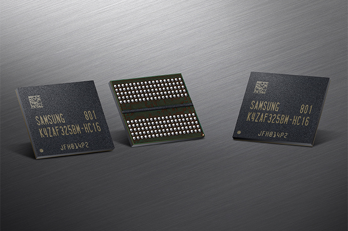
In addition to 16 Gb GDDR6 chips with 18 Gbps I/O speed, Samsung will offer GDDR6 with 12, 14 and 16 Gbps data transfer rates, thus targeting applications with different performance requirements. Also, two chip capacities (8 Gb and 16 Gb) will enable Samsung to target applications with various requirements for the amount of memory onboard.
Assuming both capacities will be made in all the speed bins, this gives the following:
Samsung’s 16 Gb GDDR6 chips could be used for various high-end products that benefit from large amounts of memory, including graphics cards and compute accelerators. By contrast, the company’s 8 Gb GDDR6 ICs will be handy for mainstream graphics cards that do not carry large amounts of memory.GPU Memory Math: Samsung GDDR6 8 Gb (1 GB) 16 Gb (2 GB) Bandwidth Per Pin (Gb/s) 12 14 16 18 12 14 16 18 B/W per Chip/Stack (GB/s) 48 56 64 72 48 56 64 72 Max Capacity 256-bit 8 GB 16 GB 384-bit 12 GB 24 GB Total Bandwidth (GB/s) 256-bit 384 448 512 576 384 448 512 576 384-bit 576 672 768 864 576 672 768 864
Samsung did not announce pricing of its GDDR6 products, but it is logical to expect 16 Gb chips with an 18 Gbps data transfer rate to cost considerably more than 8 Gb ICs with lower speed bins. Therefore, the large portfolio will enable Samsung to capitalize on the new type of memory.
Related Reading- Samsung Starts Mass Production of 16Gb GDDR6 Memory ICs with 18 Gbps I/O Speed
- Samsung Starts Production of 8 Gb DDR4-3600 ICs Using 2nd Gen 10nm-Class Tech
- Samsung Pre-Announces 16 Gbps GDDR6 Chips for Next-Gen Graphics Cards
- Micron Discusses GDDR: 16 Gbps GDDR5X, 16 nm GDDR6 and GDDR5
- SK Hynix Advances Graphics DRAM: GDDR6 Added to Catalogue, GDDR5 Gets Faster
More...
-
01-25-18, 01:51 PM #7802
Anandtech: Integral Launches 512 GB microSDXC Card: UHC-I, U1, Class 10
Integral Memory has released the industry’s highest-capacity microSDXC memory card that one can buy today. Integral’s new 512 GB microSDXC V10, UHS-I U1 card can store half of a terabyte of data, but its performance is not very high, meeting only the V10 specification for sequential write speed, limiting the recording of 4K video.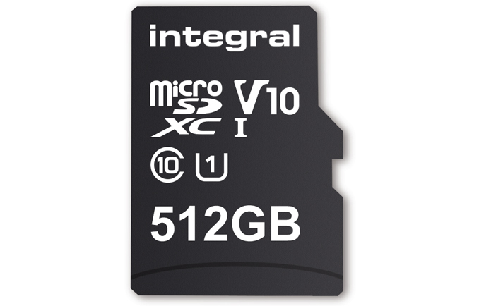
Integral’s 512 GB microSDXC card belongs to the company’s Class 10 UHS-I U1 lineup that already includes various capacities from 8 GB to 256 GB. These cards are aimed at Google Android-based smartphones, as well as tablets, and are designed primarily to store videos and images. The 512 GB microSDXC card uses the UHS-I bus and delivers up to 80 MB/s data transfer rate. The card also carries the Class 10 and UHS Speed Class U1 labels which guarantee that it supports at least 10 MB/s minimum sequential writing speed, which is enough for taking pictures and FHD videos. Meanwhile the card does not support any Application Performance Classes and therefore might not be suitable for huge mobile games or VR applications.
A number of manufacturers demonstrated microSD cards featuring 512 GB and even 1 TB capacities (some are even listed), but none of them has started commercial shipments of such products. The highest-capacity microSD card available today is the SanDisk Ultra Plus 400 GB that can be used to store applications.
Integral plans to start selling its 512 GB microSDXC V10, UHS-I U1 card sometimes in February, but says nothing about its price. Typically Integral’s microSD cards for smartphones are shipped with a USB OTG (On-The-Go) microSDHC/XC card reader featuring dual USB connectors, but it looks like in case of the 512 GB microSDXC card the company will only supply a microSD-to-SD adapter.Integral 512 GB microSD Card at a Glance General Specifications Usable Capacity ~512 GB Read Speed up to 80 MB/s Write Speed Minimum Sequential Write Speed 10 MB/s Operating Temperatures 32ºF to 140ºF (0ºC to 60C) Interface UHS-I Availability February 2018 SDA Labels UHS-I, Class 10, U1
For xkcd fans, this means that with microSD cards we can now reach 12.8 PB per gallon.
Related Reading- Western Digital Launches SanDisk Ultra microSD Card with 400 GB Capacity
- SanDisk Launches Extreme PRO SD Cards: Up to 512GB
- ADATA Demonstrates 256 GB microSDXC Card
- Sony Announces SF-G UHS-II SD Cards: Up to Nearly 300 MB/s Read/Write Performance
- ADATA Demos A2-class microSD Card with 4K/2K IOPS Minimum, Mulls Late 2017 Launch
- ADATA Launches Premier ONE UHS-II SD Cards: 3D MLC, Up to 290 MB/s, V90 Labels
More...
-
01-25-18, 03:13 PM #7803
Anandtech: SK Hynixs Product Catalog Lists 16 Gb DDR4 Chips, Opens Doors to 256 GB D
SK Hynix has recently added single-die DDR4 memory chips featuring 16 Gb capacity to its product catalog. The benefit of the increase in single-die capacity is two fold: not only will the new components enable the company to build high-capacity memory modules using fewer chips, but also it will enable SK Hynix and its partners to build 256 GB DDR4 memory modules for ultra-high-end servers.
16 Gb DRAM chips per se are not exactly a breakthrough. Memory makers, including SK Hynix, already build high-capacity DRAM components by stacking two or four 8 Gb memory dies vertically using TSVs to get 16 Gb and 32 Gb components, then use such chips to build memory modules featuring 64 GB and 128 GB density. Stacking makes organization of DIMMs very complex: in the case of a 64 GB module we are dealing with a quad-ranked DIMM (featuring two physical and two logical ranks), whereas a 128 GB module is octal ranked (featuring two physical ranks and four logical ranks). LRDIMMs have a relatively high latency in general (because they use additional buffers), meanwhile complexity of 64 GB/128 GB LRDIMM architecture forces module makers to increase them even further (to CL20/CL22 for DDR4-2400/DDR4-2666 speed bins).
By contrast, SK Hynix has managed to develop single-die 16 Gb DDR4 components. Such ICs enable producers to build client memory modules or subsystems with a fewer number of chips, lowering power consumption, and allows server-class DIMMs with densities of up to 256 GB. When it comes to servers, the 16 Gb DDR4 components will allow to build dual-ranked 64 GB modules, quad-ranked 128 GB LRDIMMs and octal-ranked 256 GB LRDIMMs.
Do not expect the 256 GB modules to show up tomorrow, but the importance of ultra-high-density LRDIMMs is hard to overestimate. For example, if the microcode is adjusted to allow it, a single socket Xeon Scalable platform featuring an -M suffixed processors with 12 total memory slots could potentially support 3 TB of six-channel memory. Meanwhile, an AMD EPYC-based system can currently support 2 TB of eight-channel memory per CPU socket, and these modules could help support double that. For in-memory applications like huge databases, the more DRAM they can get the better. Undoubtedly, 128 GB and 256 GB memory modules will come at a price. For example, Crucial sells its 128 GB DDR4-LRDIMM for $3999.99 in retail, so a 2X capacity module would cost considerably higher.
SK Hynix’s 16 Gb DDR4 chips are organized as 1Gx16 and 2Gx8 and supplied in FBGA96 and FBGA78 packages, respectively. At present, 16 Gb memory components are rated to operate in DDR4-2133 CL15 and DDR4-2400 CL17 modes at 1.2 Volts. Sometimes in the third quarter SK Hynix plans to add DDR4-2666 CL19 to the lineup. SK Hynix does not disclose which manufacturing technology it uses to make its 16 Gb chips, but it is logical to expect that the company uses a fabrication process with minimal feature sizes and high yields to make large dies.
Keep in mind that it will take quite a while for server makers to validate 16 Gb chips and 2Hi/4Hi stacks based on them, so do not expect 256 GB modules to hit today’s servers shortly from now. In the meantime, 16 Gb DDR4 chips will enable makers of SO-DIMMs to build single-sided 16 GB DDR4 SO-DIMM modules. This will also allow thin laptops (that do not use modules, but rely on commodity memory) to install 16 GB of DRAM using eight chips. For any user wondering why most 13-inch notebooks do not want to use 16 GB of DRAM in all but the high-end specification, these chips should enable a nicer ecosystem for higher memory capacity small notebooks.General Specifications of SK Hynix's 16 Gb Chips Part Number Transfer Rate Latency Org. Pkg. VDD Availability H5ANAG6NAMR-TFC 2133 MT/s 15-15-15 1Gx16 FBGA96 1.2 V Now H5ANAG6NAMR-UHC 2400 MT/s 17-17-17 H5ANAG6NCMR-UHC 2400 MT/s 17-17-17 Q3 2018 H5ANAG6NCMR-VKC 2666 MT/s 19-19-19 H5ANAG8NAMR-TFC 2133 MT/s 15-15-15 2Gx8 FBGA78 Now H5ANAG8NAMR-UHC 2400 MT/s 17-17-17 H5ANAG8NCMR-UHC 2400 MT/s 17-17-17 Q3 2018 H5ANAG8NCMR-VKC 2666 MT/s 19-19-19
Related Reading- Mega Memory: Crucial Ships 128 GB DDR4-2666 Modules for Servers at $3999 per Unit
- Intel Unveils the Xeon Scalable Processor Family: Skylake-SP in Bronze, Silver, Gold and Platinum
- Crucial Announces DDR4-2666 DIMMs for Upcoming Server Platforms
- Sizing Up Servers: Intel's Skylake-SP Xeon versus AMD's EPYC 7000 - The Server CPU Battle of the Decade?
- Dual Xeon Scalable Overclocking: ASUS WS C621E 'Sage' Workstation Motherboard Announced
- DDR4 Haswell-E Scaling Review: 2133 to 3200 with G.Skill, Corsair, ADATA and Crucial
- ASRock Rack Announces EP2C612D24 and 4L: Dual Socket Haswell-EP with 24 DDR4 Slots
More...
-
01-25-18, 10:07 PM #7804
Anandtech: Intel Announces Q4 2017 and FY 2017 Results
Today Intel announced their quarterly earnings, and 2017 was another record year for the company. Q4 revenue was a record $17.1 billion, and the full year revenue was a record $62.8 billion. For this quarter, Intel’s GAAP earnings took a hit due to a $5.4 billion tax expense thanks to the new tax reforms that were enacted in December, but as a one-time hit, it shouldn’t be a concern going forward. In fact, Intel is forecasting only a 14% tax rate for FY 2018.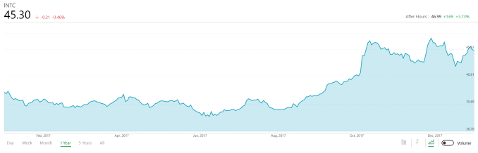
In GAAP terms, Intel’s gross margin was 63.1%, which is up 1.4% from a year ago, and their operating income was up 19% to $5.4 billion. However, thanks to a 111.4% effective tax rate due to the one time $5.4 billion tax fee, Intel is actually reporting a GAAP loss for the quarter of $0.7 billion. Earnings per share were therefore down 120% to a loss per share of $0.15.
Due to the tax impact, it’s probably a good thing to look at Non-GAAP earnings as well which will exclude that one-time charge. In terms of Non-GAAP, Intel’s gross margin was 64.8%, which was up 1.7%. Operating income was up 21% to $5.9 billion. Intel’s Non-GAAP tax rate was 21.2%, which is actually higher than the 19.8% they paid last year, and net income was $5.2 billion, up 34% from a year ago. This led to earnings per share being up 37% to $1.08.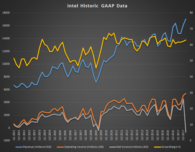
For the full year, Intel had $62.8 billion in revenue, with a gross margin of 62.3%. Operating income was up 39% year-over-year to $17.9 billion, although thanks to the tax hit their net income was down 7% to $9.6 billion. In Non-GAAP terms, net income was up 27% to $16.8 billion.
Intel is still pivoting business away from the declining PC market, and they have done well to diversify, but still, their PC business is still the biggest piece of the pie. For the quarter, the Client Computing Group had revenues of $9.0 billion, which is down 2% year-over-year, but for the full year of 2017, their CCG was up 3% to $34 billion. It’s not quite dead yet. In an effort to show their diversification, Intel is now quoting their data in “PC-centric” and “Data-centric” and conveniently, Data-centric is all of their business outside of the CCG, but even so, the CCG still accounted for 53% of Intel’s revenue for the quarter.Intel Q3 2017 Financial Results (GAAP) Q4'2017 Q3'2017 Q4'2016 Revenue $17.1B $16.1B $16.4B Operating Income $5.4B $5.1B $4.5B Net Income -$0.7B $4.5B $3.6B Gross Margin 63.1% 62.3% 61.7% Client Computing Group Revenue $9.0B +1.6% -2.0% Data Center Group Revenue $5.6B +14.7% +20.0% Internet of Things Revenue $879M +3.5% +21.0% Non-Volatile Memory Solutions Group $889M -0.2% +9.0% Programmable Solutions Group $568M +21.1% +35.0%
But, the Data-centric group is certainly growing much quicker than the PC market which is still in a decline. The Data Center Group is by far the largest portion of Intel’s Data-centric efforts, and the DCG had revenues of $5.6 billion for the quarter, which are up 20% year-over-year. With the expansion of the cloud, this likely still has some ways to go before it hits a peak, so it’s likely just a matter of time before they finally surpass their Client Computing Group.
The rest of the Data-centric business was also up for the quarter, with IoT up 20% year-over-year, to $879 million. For the full year the IoT was up 20% and had revenues of $3.2 billion. Non-volatile memory was up 9% for the quarter to $889 million, and for the year it was up 37% to $3.5 billion. Programmable Solutions was up 35% for the quarter to $568 million, and for the full year, was up 14% to $1.9 billion.
Intel still hasn’t shipped anything on 10nm, although we’re finally getting close. 14nm was delayed, but the delay in getting to 10nm has been longer than likely anyone expected. Intel has still made some bold claims about density, so it should be a good node for them if and when it arrives.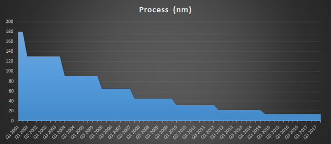
Intel’s forecast for Q1 2018 is for $15.0 billion in revenue, plus or minus $500 million, and despite the rough start to 2018, they are still forecasting another record year, with $65 billion in revenue, plus or minus $1.0 billion.
Source: Intel Investor Relations
More...
-
01-26-18, 08:15 AM #7805
Anandtech: It's An RGB Disco: The GIGABYTE X299 Gaming 7 Pro Motherboard, Reviewed
We have reviewed a lot of X299 based motherboards over the past couple of months, but our first Gigabyte/AORUS offering is the X299 Gaming 7 Pro. The G7P promises a slew of full-length PCIe slots, three M.2 slots with heatsinks, more USB 3.1 ports than most could use, and enough RGB LED lighting to have a full-on disco in a PC. See the details in our review, and bring sunglasses!
More...
-
-
01-29-18, 08:27 AM #7807
Anandtech: Solving the Automotive Bandwidth Problem: Aquantia Partners with NVIDIA fo
One of the lesser known topics around fully autonomous vehicles is one of transporting data around. There are usually two options: transport raw image and sensor data with super low latency but with high bandwidth requirements, or use encoding tools and DSPs to send fewer bits but at a higher latency. As we move into development of the first Level 4 (near autonomous) and Level 5 (fully autonomous) vehicle systems, for safety and response time reasons, low latency has won. This means shifting data around, and a lot of it.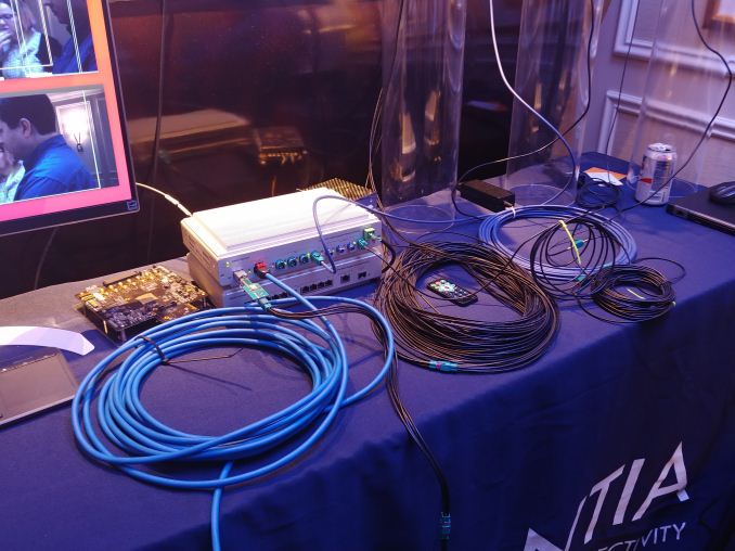
Raw camera data is big: a 1080p60 video, with 8-bits of color per channel, requires a bandwidth of 0.373 GB/s. That is gigabytes per second, or the equivalent of 2.99 gigabits per second, per camera. Now strap anywhere from 4 to 8 of these sensors on board, the switches needed to manage them, the redundancy required for autonomy to still work if one element gets taken offline, and we hit a bandwidth problem. Gigabit simply isn't enough.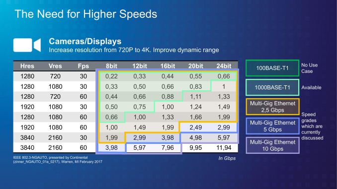
Bandwidth required, in Gbps for raw video at a given resolution and frame rate, also at a specific color depth. E.g. 720p30 at 24-bit RGB (8-bit per color) is 0.66 Gbps
The announcement today is two fold: NVIDIA and Aquantia are announcing a partnership that means Aquantia based network controllers and PHYs will be used inside NVIDIA's DrivePX Xavier platform, and subsequently the Pegasus platform as well. The second announcement is the new automotive product stack from Aquantia, AQcelerate, consisting of three chips depending on the automotive networking requirement.
For the three new chips, one is a PHY, one is a PCIe network controller, and a third combines the two. The PHY can take a standard camera inputs (2500BASE-X, USXGMII, and XFI) and send the data through multi-gigabit Ethernet as required. The controller can take standard XFI 10 Gb SerDes data and output direct to PCIe, while the combination chip is as a regular MACPHY combo, converting Ethernet data to PCIe. All three chips are built on a 28nm process (Aquantia works with both TSMC and GloFo, but stated that for these products the fab is not being announced), and qualified for the AEC-Q100 industry standard.Aquantia AQcelerate for Automotive Type Input Output Use Case Package Size
(FCBGA)AQC100 PHY 2500Base-X
USXGMII
XFI
KR10GbE
5GbE
2.5GbEADASCamerasParking AssistSensorsTelematicsAudio/VideoInfotainment- AQVC100 MAC XFI PCIe 2/3 x2/x4 7x11 mm AQVC107 Both PCIe 2/3
x1/x2/x410GbE
5GbE
2.5GbE12x14 mm
The benefits of using multi-gigabit, as explained to us by Aquantia, is that it allows for a 2.5G connection using only a standard twisted pair cable, or 5G for dual pair, up to 10G for quad pair. Current automotive networking systems are based on single pair 100/1000Mbit technology, which is insufficient for the high bandwidth, low latency requirements that companies like NVIDIA put into their Level 4/5 systems.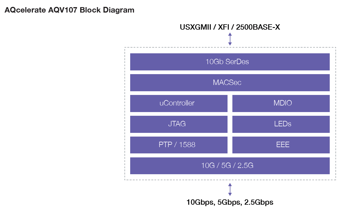
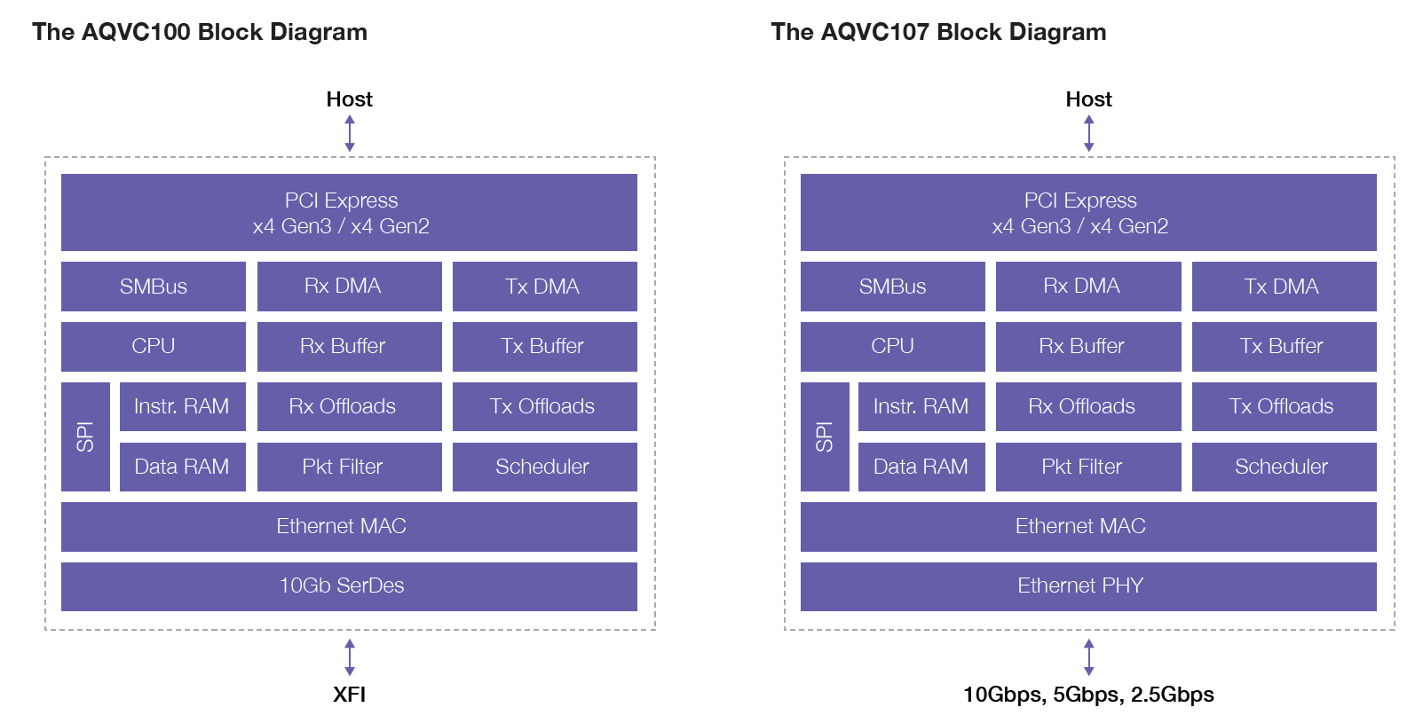
Click to enlarge block diagrams
These chips were designed on Aquantia's roadmap before its collaboration with NVIDIA, however NVIDIA approached Aquantia looking for something to work, given Aquantia's current march on multi-gigabit Ethernet ahead of its rivals. We are told that the silicon doesn't do anything special and specific with NVIDIA, allowing other companies keen on automotive technology to use Aquantia as well. With Aquantia's lead in the multi-gigabit Ethernet space, over say Intel, Qualcomm, and Realtek, it seems that the only option at this point for wired connectivity, if you need to send raw data, is something like this. However, the lead time for collaboration seems to be substantial: Aquantia stated that NVIDIA's Gary Shapiro recorded promotional material for them in the middle of last year, however Xavier was announced in 2016, so it is likely that Aquantia and NVIDIA were looking at integration before then.
A quick side discussion on managing all this data. If there is 16 GB/s from all the sensors flying around, the internal switches and SoCs has to be able to handle it. At CES, NVIDIA provided a base block diagram of an Xavier SoC, including some details about its custom ARM cores, its GPU, the DSPs, and some about the networking.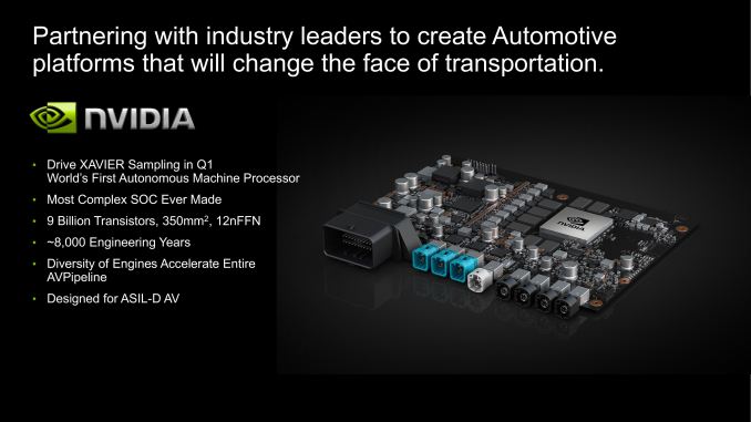
The slide shows that the silicon has gigabit and 10 gigabit embedded in (so it just needs a PHY to work), as well as 109 Gbps total networking support. On the Video Processor, it supports 1.8 gigapixel/s decode, which if we plug in some numbers (1080p60 = 124MPixel/s) allows for about a dozen or so cameras at 8bit color, or a combination of 4K cameras and other sensors. The images of the Xavier also show the ISP, capable of 1.5 gigapixel/s.
An mockup example from Aquantia showed a potential Level 4/5 autonomous arrangement, with 10 RADAR/LIDAR/SONAR sensors, 8 cameras, and a total of 18 PHYs, two controllers, and three switches. Bearing in mind that there is a level of redundancy for these systems (cameras and sensors should connect two at least two switches, if one CPU fails than another can take over, etc), then this is a lot of networking silicon to go into a single car, and a large potential for anyone who can get the multi-gigabit data transfer done right. The question then comes down to power, which is something Aquantia is not revealing at this time, instead preferring to allow NVIDIA to quote a system wide level power.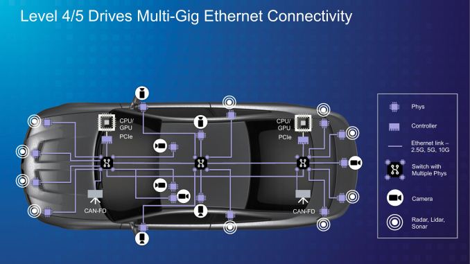
The image at the top is the setup shown to us by Aquantia at CES, demonstrating a switch using AQcelerate silicon capable of supporting various cables, including the vital 2.5 Gbps over a single pair.
Related Reading- Aquantia Launches New 2.5G/5G Multi-Gigabit Network Controllers for PCs
- Aquantia Launch AQtion 5G/2.5G/1G Multi-Gigabit Ethernet Cards (NICs) for PCIe
- Lower Cost 10GBase-T Switches Coming: 4, 5 and 8-port Aquantia Solutions at ~$30/Port
- Dell Now Offers Aquantia AQtion AQN-108-Based 5 GbE Cards with Select PCs
More...
-
01-29-18, 08:27 AM #7808
Anandtech: The EVGA X299 FTW K Motherboard Review: Dual U.2 Ports
The EVGA X299 FTW K is our first X299 motherboard from EVGA. The FTW K aims to bring users a solid power delivery, three-way multi-GPU capabilities, two M.2 slots, and a unique feature so far on our X299 coverage: two U.2 ports. The X299 FTW K looks to fit into the crowded mid-range segment for X299 motherboards at its price point. We will put it on the test bed and gave it a thorough inspection.
More...
-
01-29-18, 10:46 AM #7809
Anandtech: NEC 2018 LaVie Note Mobile: Fanless 12.5 Core i7 with 12hr Battery, Under
This month, NEC has introduced its first 2018 LaVie notebook: The LaVie Note Mobile. The LaVie line is known due to its design philosophy of being lightweight: when we had a chance to hold the LaVie Z back in 2015, it was so light it felt like picking up an empty shell of a system. For 2018, the Lavie Note Mobile is the newest member of the family, being updated from the previous model. This design has a 12.5-inch screen, and since Intel has not released any new ultra-low-voltage CPUs recently, NEC had to retain usage of Kaby Lake-Y SoCs. Despite featuring a larger LCD, the new 2018 Lavie Note Mobile still weighs in the range of two pounds (~900 grams) and is rated to work for nearly 12 hours on one battery charge.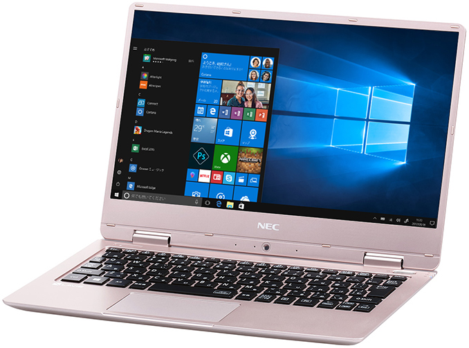
NEC’s Lavie Note Mobile is the company’s most compact laptop lineup. The previous-gen Lavie Note Mobile came with 11.6” IGZO IPS FHD displays, but for the 2018 (NMx50/KA) family NEC decided to update it in three ways: an 12.5” IPS FHD monitor, reduce the system’s thickness to 17 mm, and increase the amount of DRAM on high-end models. The LCD gained nearly an inch of real estate, but lost its IGZO material in the process. Compared with the 2017 model, it is worth noting that the updates cause a couple of minor changes: the 11.7-hour rated battery life is slightly down from 13, and the weight is slightly up by a few grams.
The increase of the display size, reduced thickness and enhanced RAM size will make the new Lavie Note Mobile more competitive against ultra-compact products like Apple’s MacBook, so NEC’s design decisions look rather logical. As for visual aesthetics, NEC also adjusted its Lavie Note Mobile lineup this year: the new notebooks will be available in pink, pearl white and pearl black.
Overall other specifications of the 2018 NEC Lavie Note Mobile range are similar to the 2017 versions: at retail, available systems are based on Intel’s Kaby Lake-Y SoCs: the Core i5-7Y54, the Core m3-7Y30 or the Celeron 3965Y. In order to get the Core i7-7Y75 model, according to PC Watch, the unit has to be bought directly from NEC. The Kaby Lake-Y SoCs feature two cores, Intel’s UHD Graphics 615, and are around 4.5 W rated TDP, which is of course their main feature that enables NEC to use passive cooling. The new Lavie Note Mobile machines are equipped with 4 or 8 GB of dual-channel LPDDR3 memory (up from 4 GB on previous-generation Lavie NM laptops), as well as a Samsung PM871b SATA SSD featuring 64 GB, 128 GB or 256 GB capacity. The higher-end Core i7-based SKU also has a 512 GB PCIe SSD option.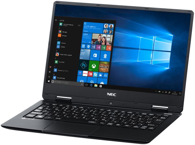
When it comes to connectivity and I/O interfaces, everything looks pretty standard: the NEC Lavie Note Mobile laptops are equipped with a 802.11ac + Bluetooth 4.1 wireless module, two USB 3.0 Type-A ports, a 3.5-mm TRRS audio connector, a Windows Hello-compatible fingerprint reader, an HDMI output, a webcam located under the display, a built-in microphone, stereo speakers, an SD card reader and so on. All the physical ports are located on the backside of the notebook. Some might consider the lack of a USB Type-C port in 2018 a drawback.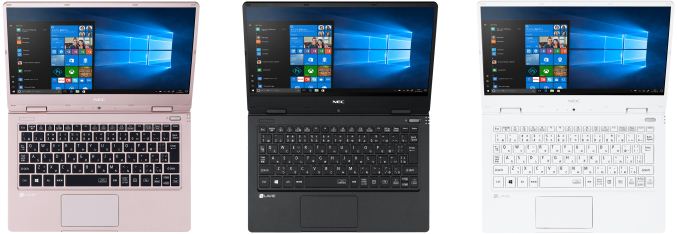
A sharp-eyed reader might also notice a rather small space bar that is barely six centimeters long. While this looks like a problem for people using European languages, this is not a problem for Japanese, who do not have to use spaces often, which is why short spacebars are common on laptops for the Land of the Rising Sun.
NEC’s Lavie Note Mobile is already available. The most affordable Celeron-based model costs ¥104,800 ($963), whereas the more advanced Core i5-powered SKU is priced at ¥144,800 ($1330).The NEC Lavie Note Mobile General Specifications NM550/KA NM350/KA NM150/KA Display 12.5" non-glossy IPS
1920×1080 resolutionSoC Core i5-7Y54
Core i7-7Y75*Core m3-7Y30 Celeron 3965Y RAM 8 GB LPDDR3 4 GB LPDDR3 Storage 256 GB SSD SATA
512 GB SSD PCIe*128 GB SSD SATA 64 GB SSD SATA Camera 720p webcam Wireless 802.11ac Wi-Fi
867 Mbps
Bluetooth 4.1802.11ac Wi-Fi
433 Mbps
Bluetooth 4.1I/O ports 2 × USB 3.0 Type-A
1 × HDMI
SD card readerAudio Integrated speakers
1 × TRRS 3.5-mm jack for headset
Yamaha AudioEngine software enhancementsDimensions 289 × 197.5 × 17 mm Weight 904 - 925 grams Battery unknown OS Windows 10 Home
Windows 10 Pro*Fingerprint Yes Finish Pink
Black
WhitePrice ¥144,800 ($1330) ¥124,800 ($1148) ¥104,800 ($963) Notes *Available only directly from NEC
Related Reading- Acer’s New Swift 7 Gets 14-inch Display, LTE Modem, Becomes Thinner & Pricier
- Fujitsu Announces 13.3" Lifebook U937/P and UH75/B1: 7th Gen Core i5, 8hr Battery, Under 1.77 lbs
Sources: NEC, PC Watch.
More...
-
01-29-18, 08:46 PM #7810
Anandtech: Samsung Launches Z-SSD SZ985: Up To 800GB Of Z-NAND
Samsung announced today that they are officially launching their first Z-SSD product, the SZ985. The Z-SSD uses Samsung's Z-NAND memory, a high-performance derivative of their 3D NAND flash memory and Samsung's intended competition for Intel's 3D XPoint memory. The SZ985 is a high-performance, high-endurance enterprise NVMe SSD.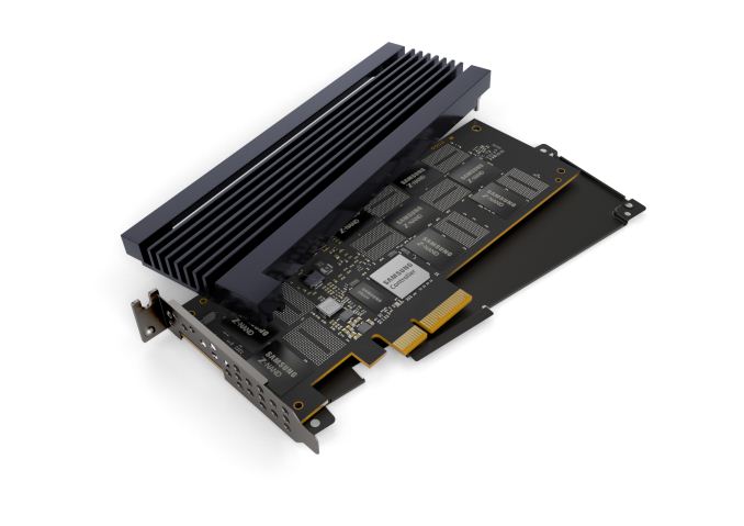
Samsung has been talking about Z-NAND and the SZ985 for quite a while, including showing off prototypes at several trade shows and conferences. Their initial announcement in 2016 of Z-NAND memory and Z-SSD drives promised 1TB drives in 2016 to be followed by 2TB and 4TB drives in 2017. Today's launch of 800GB and 240GB models is far behind that initial timeline, but the Z-SSD is finally ready for broad release, almost a year after Intel's Optane products first hit the shelves. Samsung hasn't provided much new information about how the Z-SSD works under the hood, but they have disclosed that the drive includes 1.5GB of LPDDR4 DRAM. This suggests that the Z-SSD either has huge overprovisioning with as much as 1.5TB or Z-NAND memory for the 800GB model, or that the Z-NAND is being managed in a way that requires more than the usual 1GB of DRAM per TB of NAND flash used by most SSDs.
Samsung has not provided full performance specifications for the SZ985, but they have highlighted several key metrics that put the Z-SSD in the top performance tier. The SZ985 can deliver up to 750k random read IOPS, well above the 550k IOPS that Intel's Optane SSD DC P4800X is rated for. Write performance from the SZ985 is much less impressive at only 170k random write IOPS. The random write speed rating on Intel's P4800X is only 9% slower than the random read speed, while the Samsung SZ985 will have a random write speed that is 77% slower than random reads. Samsung has not been able to overcome all of the limitations of flash memory, but they have produced some impressive improvements.
Samsung also makes a few comparisons against more mainstream enterprise SSDs based on 3D TLC NAND flash memory. The memory cell read performance of their Z-NAND is ten times higher than their 3D TLC NAND, leading to 70% higher random read throughput than their PM963 NVMe SSD. Exact read latency isn't specified, but write latency on the SZ985 is quoted as 16 µs.
Despite not having record-setting write performance, the SZ985 is still designed to handle very write-intensive workloads. The endurance rating is 30 drive writes per day for five years, matching Intel's Optane SSD. However, both drives still fall short of the long-gone Micron P320h SLC NAND SSD, in both performance and endurance (though Intel has at least exceeded the random write speed of the P320h). Samsung's most significant accomplishment with the Z-SSS SZ985 is likely that they can offer the performance of planar SLC at much lower cost thanks to their 3D NAND structure.
Samsung will be presenting the Z-SSD SZ985 at the International Solid-State Circuits Conference, February 11-15.
At Flash Memory Summit last year, Samsung announced a second generation of Z-NAND memory. The SZ985 is still a first-generation product, and drives with the second-generation Z-NAND could still be a long way from launching.
More...


 Quote
Quote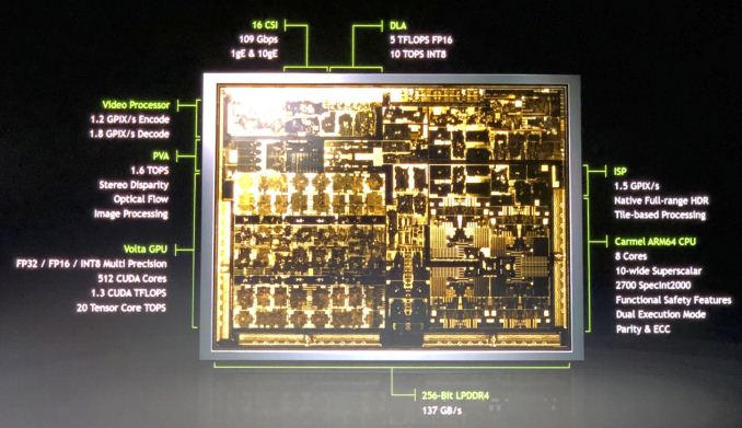
Thread Information
Users Browsing this Thread
There are currently 12 users browsing this thread. (0 members and 12 guests)


Bookmarks