

Results 7,851 to 7,860 of 12096
Thread: Anandtech News
-
02-12-18, 03:16 PM #7851
Anandtech: Micron Readies 3D QLC NAND-Based Datacenter SSDs for Nearline Storage
Micron has revealed plans to release datacenter-class SSDs based on 3D QLC NAND memory in an effort to compete in the nearline storage market. Briefly announced at a conference last week, the company is taking aim at applications that currently use 7200 RPM HDDs, the use of which is increasingly common in nearline storage. The manufacturer did not reveal any additional details about the upcoming drive, but demonstrated a wafer with QLC 3D NAND dies.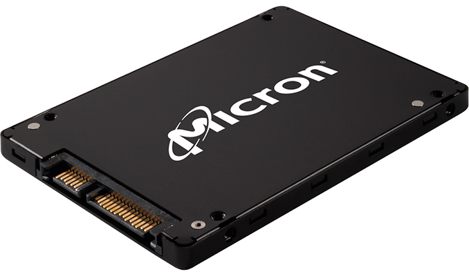
Micron disclosed its plans concerning own-brand SSDs in 2018 at the A3 Technology Live conference in London last week. Among other things, the company intends to introduce a QLC-based SSD with a SATA interface for cloud datacenters this year. The drive will be positioned below the existing 5200-series SSDs and will be aimed primarily at read intensive applications (or the so-called WORM — write once, read many workloads). The QLC-based SSD will have a feature set aimed at hyperscale datacenters and will compete for the place currently occupied by high-capacity 7200 RPM HDDs, reports The Register.
The manufacturer did not disclose capacity of the upcoming QLC-based drives and did not reveal whether they will feature in-house developed controllers with enhanced ECC capabilities (developed using IP and engineers the company got when it acquired Tidal Systems several years ago), or third-party enterprise-grade controllers. The company demonstrated a wafer carrying 64 GB (i.e., 512 Gb) 3D QLC NAND chips, indicating that it has the new flash memory at hand already.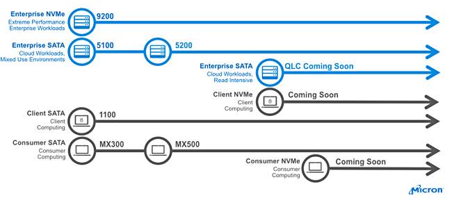
QLC flash memory stores four bits per cell, thus offering a 33% higher bit density and lower per-bit cost compared to TLC flash commonly used for high-capacity SSDs today. 3D QLC NAND has been formally announced by Toshiba and Western Digital so far, but there are no doubts that all producers of NAND are working on QLC chips too. Increasing the bit density of NAND flash usually comes at the cost of endurance, but Toshiba last year said that it had managed to increase endurance of its 3D QLC NAND flash to 1000 program/erase cycles by using a stronger ECC mechanism, which is comparable to endurance of 3D TLC NAND.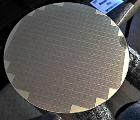
QLC’s higher bit densities as well as lower per-bit costs are expected to reduce per-GB prices of high-capacity SSDs further and enable them to compete against existing leading-edge HDDs, such HGST’s Ultrastar with 12 or 14 TB capacity. Two obvious advantages that high-capacity QLC-based SSDs will have when compared to hard drives are lower latencies and higher storage densities. Meanwhile, per-GB costs of HDDs will remain lower when compared to NAND flash for years to come — this is what producers of both HDDs and flash memory agree on. So I'd expect to see that these upcoming 3D QLC NAND-based SSDs will sit between high-capacity HDDs and high-performance SSDs, occupying a tier of their own in hyperscale datacenters.
Related Reading:
- Western Digital Announces Four Bit Per Cell 64-Layer 3D NAND Flash
- Toshiba's 768Gb 3D QLC NAND Flash Memory: Matching TLC at 1000 P/E Cycles?
- Micron 2017 Roadmap Detailed: 64-layer 3D NAND, GDDR6 Getting Closer, & CEO Retiring
- Micron 3D NAND Update: 2D and 3D NAND Bit Crossover, Gen 2 Hits Production
Sources: The Register, A3 Communications Technology Live
More...
-
02-13-18, 08:10 AM #7852
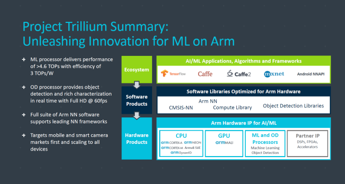
Anandtech: ARM Announces Project Trillium Machine Learning IPs
Today’s Arm announcement is a bit out of the norm for the company, as it’s the first in a series of staggered releases of information. For this first announcement Arm is publicly unveiling “Project Trillium” – a group of software solutions as well IP for object detection and machine learning.
Machine learning is indeed the hot new topic in the semiconductor business and has particularly seen a large focus in the mobile world over the last couple of months, with announcements from various IP companies as well as consumer solutions from the likes of Huawei. We’ve most recently had a more in-depth look and exploration of the topic of machine learning and neural network processing in a dedicated section of our review of the Kirin 970.
Whilst we had a great amount of noise from many industry players on the topic of machine learning IPs. Arm was conspicuously absent from the news and until now the focus has been on the CPU ISA extensions of Armv8.2, which introduce specialised instructions which simplify and accelerate implementations of neural networks with the help of half-precision floating point and integer dot products.
Alongside the CPU improvements we've also seen GPU improvements for machine learning in the G72. While both of these improvements help, they are insufficient in use-cases where maximum performance and efficiency are required. For example, as we’ve seen in the our test of the Kirin 970’s NPU and Qualcomm’s DSP – the efficiency of running inferencing on specialized IPs is above an order of magnitude higher than running it on a CPU.
As Arm explains it, the Armv8.2 and GPU improvements were only the first results towards establishing solutions for machine learning, while in parallel they’ve examined the need for dedicated solutions. Industry pressure from partners made it clear that the performance and efficiency requirements made dedicated solutions inevitable and started work on its machine learning (ML) processors.
Today’s announcement covers the new ML processors as well as object detection processors (OD). The latter IP is a result of Arm’s Apical acquirement in 2016 which saw the company add solutions for the display and camera pipelines to their IP portfolio.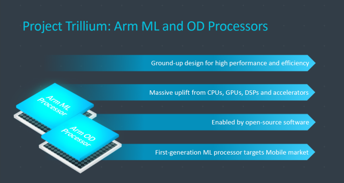
Starting with the ML processor – what we’re talking about here is a dedicated IP for neural network model inferencing acceleration. As we’ve emphasised in our NN related announcements of late, Arm also emphasises that having an architecture which is specifically designed for such workloads can have significant advantages over traditional CPU and GPU architectures. Arm also made a great focus on the need to design an architecture which is able to do optimised memory management of the data that flows through a processor when executing ML workloads. These workloads have high data reusability and minimising the in- and out-bound data through the processor is a key aspect of reaching high performance and high efficiency.
Arm’s ML processor promises to reach theoretical throughput of over 4.6TOPs (8-bit integer) at target power envelopes of around 1.5W, advertising up to 3TOPs/W. The power and efficiency estimates are based on a 7nm implementation of the IP.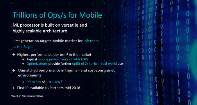
In regards to the performance figures, Arm agrees with me that the TOPs figure alone might not be the best figure to represent performance of an IP; however it’s still useful until the industry can work towards some sort of standardisation for benchmarking on popular neural network models. The ML processor can act as a fully dedicated and standalone IP block with its own ACE-Lite interface for incorporation into a SoC, or it can be integrated within DynamiQ cluster, which is a lot more novel in terms of implementation. Arm wasn’t ready to disclose more architectural information of the processor and reserves that for future announcements.
An aspect that seemed confusing is Arm’s naming of the new IP. Indeed Arm doesn’t see that the term “accelerator” is appropriate here as traditionally accelerators for Arm meant things such as packet handling accelerators in the networking space. Instead Arm sees the new ML processor as a more fully-fledged processor and therefore deserving of that naming.
The OD processor is a more traditional vision processor and is optimised for the task of object detection. There is still a need for such IP as while the ML processor could do the same task via neural networks, the OD processor can do it faster and more efficiently. This showcases just how far the industry is going to make dedicated IP for extremely specialised tasks to be able to extract the maximum amount of efficiency.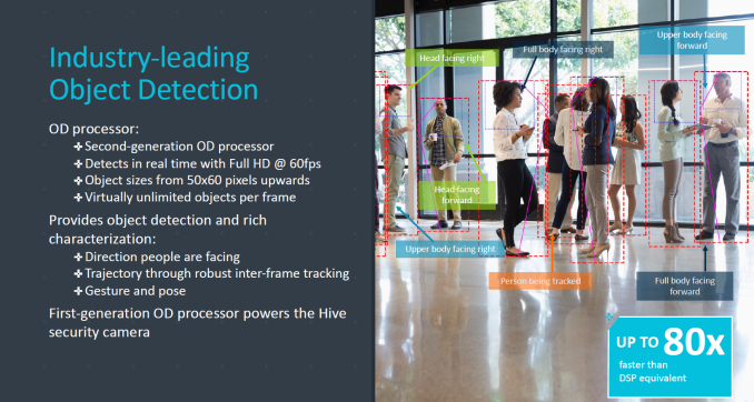
Arm envisions use-cases where the OD and ML processors are integrated together, where the OD processor would isolate areas of interest within an image and forward them to the ML processor where more fine-grained processing is executed on. Arm had a slew of fun examples as ideas, but frankly we still don’t know for sure how use-cases in the mobile space will evolve. The same can’t be said about camera and surveillance systems where we the opportunity for continuous use of OD and ML processing.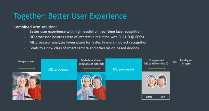
Arm’s first generation of ML processors is targeted at mobile use while variants for other spaces will follow on in the future. The architecture of the IP is said to be scalable both upwards and downwards from the initial mobile release.
As part of Project Trillium, Arm also makes available a large amount of software that will help developers implement their neural network models into different NN frameworks. These are going to be available starting today on Arm’s developer website as well as Github.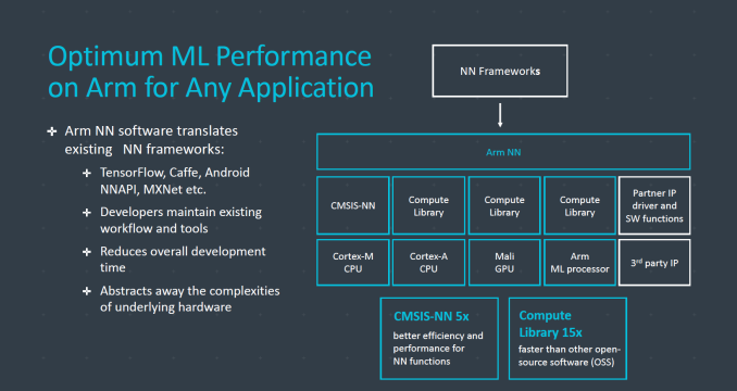
The OD processor is targeted for release to partners in Q1 while the ML processor is said to be ready mid 2018. Again this is highly unusual for Arm as usually public announcements happen far after IP availability to customers. Due to the nature of SoC development we should thus not expect silicon based on the new IP until mid to late 2019 at the earliest, making Arm one of the slow-adopters among the semiconductor IP vendors who offer ML IP.
Related Reading- HiSilicon Kirin 970 - Android SoC Power & Performance Overview
- Imagination Joins the AI Party, Announces PowerVR Series 2NX Neural Network Accelerator
- CEVA Launches Fifth-Generation Machine Learning Image and Vision DSP Solution: CEVA-XM6
- CEVA Announces NeuPro Neural Network IP
More...
-
02-13-18, 11:05 AM #7853
Anandtech: Gen-Z Interconnect Core Specification 1.0 Published
The first major release of the Gen-Z systems interconnect specification is now available. The Gen-Z Consortium was publicly announced in late 2016 and has been developing the technology as an open standard, with several drafts released in 2017 for public comment.
Gen-Z is one of several standards that emerged from the long stagnation of the PCI Express standard after the PCIe 3.0 release. Technologies like Gen-Z, CAPI, CCIX and NVLink seek to offer higher throughput, lower latency and the option of cache coherency, in order to enable much higher performance connections between processors, co-processors/accelerators, and fast storage. Gen-Z in particular has very broad ambitions to blur the lines between a memory bus, processor interconnect, peripheral bus and even straying into networking territory.
The Core Specification released today primarily addresses connecting processors to memory, with the goal of allowing the memory controllers in processors to be media-agnostic: the details of whether the memory is some type of DRAM (eg. DDR4, GDDR6) or a persistent memory like 3D XPoint are handled by a media controller at the memory end of a Gen-Z link, while the processor itself issues simple and generic read and write commands over the link. In this use case, Gen-Z doesn't completely remove the need for traditional on-die memory controllers or the highest-performance solutions like HBM2, but Gen-Z can enable more scalability and flexibility by allowing new memory types to be supported without altering the processor, and by providing access to more banks of memory than can be directly attached to the processor's own memory controller.
At the lowest level, Gen-Z connections look a lot like most other modern high-speed data links: fast serial links, bonding together multiple lanes to increase throughput, and running a packet-oriented protocol. Gen-Z borrows from both PCI Express and IEEE 802.3 Ethernet physical layer (PHY) standards to offer per-lane speeds up to the 56Gb/s raw speed of 50GBASE-KR, and will track the speed increases from future versions of those underlying standards. The PCIe PHY is incorporated more or less as-is, while the Ethernet PHY standards have been modified to allow for lower power operation when used for shorter links within a single system, such as communication between dies on a multi-chip module. Gen-Z allows for asymmetric links with more links and bandwidth in one direction than the other. The Gen-Z protocol supports various connection topologies like basic point to point links, daisy-chaining, and switched fabrics, including multiple paths of connection between endpoints. Daisy-chain links are estimated to add about 5ns of latency per hop, and switch latencies are expected to be on the order of 10ns for a small 8-port switch up to 50-60ns for a 64-port switch, so using Gen-Z for memory access is reasonable, especially where the somewhat slower persistent memory technologies are concerned. The Gen-Z protocol expresses almost everything in memory terms, but with each endpoint performing its own memory mapping and translation rather than attempting to form a unified single address space across a Gen-Z fabric that could scale beyond a single rack in a data center.
Wide Industry Participation
The Gen-Z Consortium launched with the support of a dozen major technology companies, but its membership has now grown to the point that it is easier to list the big hardware companies who aren't currently involved: Intel and NVidia. Gen-Z has members from every segment necessary to build a viable product ecosystem: semiconductor design and IP (Mentor, Cadence, PLDA), connectors (Molex, Foxconn, Amphenol, TE), processors and accelerators (AMD, ARM, IBM, Cavium, Xilinx), switches and controllers (IDT, Microsemi, Broadcom, Mellanox), every DRAM and NAND flash memory manufacturer except Intel, software vendors (RedHat, VMWare), system vendors (Lenovo, HPE, Dell EMC). It is clear that most of the industry is paying attention to Gen-Z, even if most of them haven't yet committed to bringing Gen-Z products to market.
At the SuperComputing17 conference in November, Gen-Z had a multi-vendor demo of four servers sharing access to two pools of memory through a Gen-Z switch. This was implemented with heavy use of FPGAs, but with the Core Specification 1.0 release we will start seeing Gen-Z show up in ASICs. The focus for now is on datacenter use cases with products potentially hitting the market in 2019.
In the meantime, it will be interesting to see where industry support concentrates between Gen-Z and competing standards. Many companies are members or supporters of more than one of the new interconnect standards, and there's no clear winner at this time. Nobody is abandoning PCI Express, and it isn't clear which new interconnect will offer the most compelling advantages over the existing ubiquitous standards or over proprietary interconnects. Gen-Z seems to have one of the widest membership bases and the widest target market, but it could still easily be doomed to niche status if it only receives half-hearted support from most of its members.
More...
-
02-13-18, 11:05 AM #7854
Anandtech: Panasonic Unveils Lets Note SV7: 12.1-Inch, Quad-Core CPU, TB3, ODD, 21 H
Panasonic has upgraded its 12.1-inch series laptops with Intel’s quad-core 8th Generation Core i5/i7 CPUs. The new Panasonic Let’s Note CF-SV7-series notebooks are the only ultra-compact PCs to feature Intel’s latest mobile processors, a Thunderbolt 3 interconnection, an optical drive and an optional LTE modem in a package that weighs from 999 grams to 1.124 kilograms (2.2 – 2.47 pounds).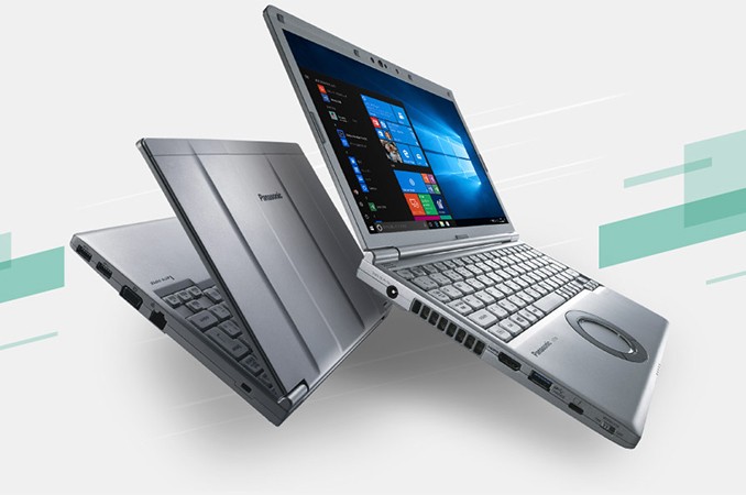
Panasonic is one of a few companies nowadays that offers highly-integrated ultra-compact laptops with optical disc drives. These machines are very light because they are made of plastic (they are still rugged enough and can be dropped from a height of 76 cm) and their weight is about a kilogram, but they are not ultra-thin like modern notebooks from Apple, HP or Lenovo. To a large degree, they are relatively thick because they are designed to offer their owners the best possible connectivity, feature set and battery life, something that we usually see on 14”/15.6” laptops from other manufacturers. In Europe and the U.S. many people nowadays prefer ultra-thin PCs even if they lack replaceable batteries or certain ports (and I am not even talking about laptops with ODDs — they have become exotic). User preferences are different in Japan, which is why Panasonic still offers 12”-class laptops with optical drives, thick replaceable batteries and plenty of connectors.
The Panasonic Let’s Note CF-SV7 family of notebooks succeeds the company’s Let’s Note CF-SZ6 lineup that featured a similar appearance, a 12.1” WUXGA (1920×1200) display, comparable weight and dimensions as well as a very long battery life of up to 21 hours (enabled by a removable accumulator). Meanwhile, even though the CF-SV7 continues traditions of the CF-SZ6, it does not mean that Panasonic just installed new quad-core CPUs into an old chassis.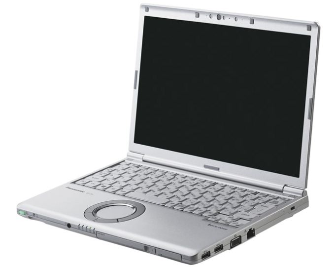
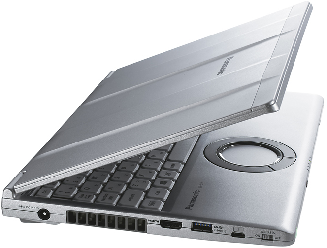
The Let’s Note SV7-series based on Intel’s quad-core Core i5/i7 processors actually uses a new chassis that is 24.5 mm thick (down from 25.3 mm in case of the SZ6) and features a new cooling system for its new CPUs. Because of the new cooler, the SV7 PCs are a bit heavier than their predecessors, but even when equipped with a high-capacity “L” battery, their weight does not exceed 1.124 kilograms. Besides the new quad-core 8th Generation Core i5/i7 processors, Panasonic’s latest SV7-series laptops obtained a Thunderbolt 3 port, a rare feature for 12”-class mobile computers.
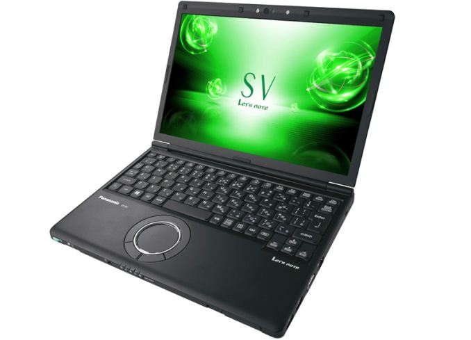
Exact configurations of Panasonic’s Let’s Note CF-SV7 vary greatly. Retail versions of the CF-SV7 are equipped with Intel’s Core i5-8250U or Core i7-8550 CPUs, 8 GB of LPDDR4-1866 memory and a SATA SSD (128 GB – 1 TB). Meanwhile, built-to-order models bought directly from Panasonic can be customized to feature Intel’s Core i5-8350U or Core i7-8650U, 16 GB RAM as well as a 1 TB PCIe SSD. As for connectivity, the systems are outfitted with an 802.11ac + Bluetooth 4.1 wireless module, a GbE connector, three USB 3.0 Type-A ports, a D-Sub output, an HDMI 2.0 header (supporting 4Kp60 resolution), a TRRS audio connector and so on. In addition, the systems feature stereo speakers, a microphone, a 720p webcam with an IR sensor compatible with Windows Hello, an SD card reader supporting SDHC/SDXC cards with UHS-II interface as well as a CD/DVD burner/reader or a Blu-ray reader/CD/DVD burner. Some systems come with a 4G/LTE modem, other can be configured to include a 1 TB HDD in addition to a 128 GB SSD. It is noteworthy that the width of a key on SV7’s keyboard is 19 mm, comparable to that of a modern MacBook Pro. Meanwhile, the new SV7 continues to feature Panasonic’s round touchpad that does not look too comfy.
Besides high integration, the Let’s Note CF-SV7-series can be proud of its battery life. When equipped with an “S” battery and an SSD, the laptop can work for up to 14 hours, according to Panasonic. Meanwhile, if an “L” accumulator is installed, the system is rated for 21 hours, probably a record for 12”-class PCs in general.
As mentioned above, Panasonic’s Let’s Note CF-SV7 laptops will come in different configurations. A basic one featuring Intel’s Core i5-8350U, 8 GB of RAM, a 256 GB SSD, a DVD drive and an “S” battery pack costs ¥253,584 w/taxes (~$2320) when bought online. A premium one equipped with Intel’s Core i7-8650U, 16 GB of RAM, a 1 TB SSD, a Blu-ray drive, an LTE modem and an “S” battery is priced at ¥425,304 w/taxes (~$3880) when bought directly from Panasonic. The Let’s Note CF-SV7 PCs are definitely priced well above average, but the systems offer unique features that tend to cost a lot.General Specifications of Panasonic Let's Note CF-SV7-Series "High-End" "Mainstream" "Entry" Display 12.1" non-glossy
1920×1200 resolutionSoC Core i7-8550U
Core i7-8650U*Core i5-8250U
Core i5-8350U*RAM 8 GB LPDDR3
16 GB LPDDR3*Storage 256 - 512 GB SSD SATA
up to 1 TB SSD PCIe*128 - 256 GB SSD SATA
up to 1 TB SSD PCIe*1 TB HDD
128 GB SSD + 1 TB HD*
up to 1 TB SSD PCIe*ODD CD/DVD burner
BD reader/CD/DVD burner*
No ODD*- Camera 720p webcam with IR sensor for Windows Hello Wireless 802.11ac Wi-Fi
Bluetooth 4.1
optional 4G/LTE modem 300/50 MbpsI/O ports 3 × USB 3.0 Type-A
1 × Thunderbolt 3/USB Type-C
1 × HDMI
1 × D-Sub
1 × GbE
SD card reader with UHS-II supportAudio Integrated speakers and microphone
1 × TRRS 3.5-mm jack for headsetDimensions 283.5 × 203.8 × 24.5 mm Weight 999 - 1124 grams Battery Life Based on JEITA 2.0 Up to 21 hours with L battery and SSD
Up to 14 hours with S battery and SSD
Up to 11 hours with S battery and HDDOS Windows 10 Pro Windows 10 Home
Windows 10 ProWindows 10 Pro Finish Body: Silver or Black*
Top Cover: Silver, Black*, Blue*, Dark Red*Notes *Available only directly from Panasonic
Related Reading:
- NEC 2018 LaVie Note Mobile: Fanless 12.5” Core i7 with 12hr Battery, Under 2 Lbs
- Acer’s New Swift 7 Gets 14-inch Display, LTE Modem, Becomes Thinner & Pricier
- Fujitsu Announces 13.3" Lifebook U937/P and UH75/B1: 7th Gen Core i5, 8hr Battery, Under 1.77 lbs
Sources: Panasonic, PC Watch
More...
-
02-13-18, 12:09 PM #7855
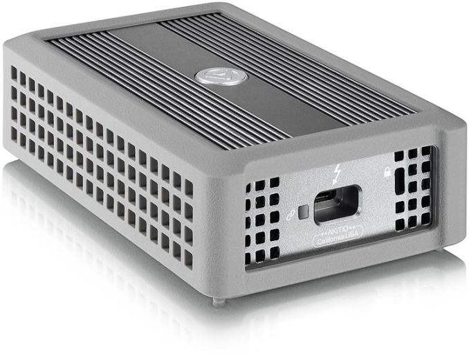
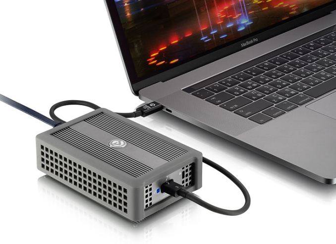
Anandtech: AKiTiOs Thunder3 10G Adapter Now Available: TB3-to-10GbE for Sub-$300
AKiTiO has quietly begun to sell its Thunderbolt 3 to 10 GbE network adapter, which it first demonstrated at Computex 2017. The device is based on a 10 GbE solution from Tehuti Networks and is compatible with both Macs and Windows PCs. Priced at just under $300, AKiTiO is selling the adapter directly as well as through Amazon.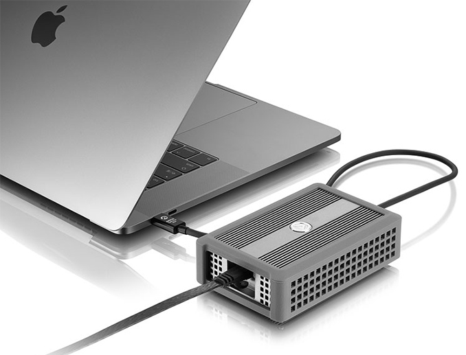
As described back in June, the AKiTiO Thunder3 10G (T3NA-T3LNITY-AKT) network adapter supports five speeds, including 10GBase-T as well as NBase-T, allowing it to work not only with corporate 10 GbE networks, but also with upcoming 2.5GBase-T and 5GBase-T networks primarily aimed at small businesses and consumers, as well as existing 1 GbE and 100 M networks. The device itself is a relatively small rugged box made of aluminum for better heat dissipation and featuring rubber pads on its sides for further protection.
The adapter is bus-powered, it only has one 10 GBase-T port, a Thunderbolt 3 header, as well as an opening for a security lock. Unlike many other TB3 devices, this one does not have another TB3 connector to daisy chain it with other TB3 appliances, perhaps to reduce development and BOM costs (more on this later), or address security concerns of certain clients. Theoretically, it should be possible to plug the Thunder 10G network adapter at the end of a Thunderbolt 3 daisy chain after a display and a DAS, but AKiTiO does explicitly list this as supported.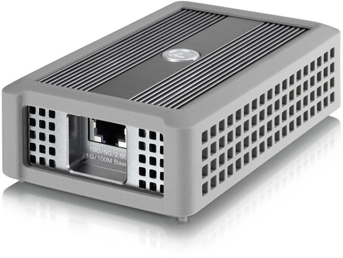
The AKiTiO Thunder3 10G (T3NA-T3LNITY-AKT) is based on Tehuti Networks’ TN9710x-TB3 reference design for Thunderbolt 3 to 10GBase-T/NBase-T network adapters. This reference design is intended to minimize the number of chips and components required: it carries Tehuti’s own TN4010 MAC, Marvell’s Alaska X 88X3310P 10 GbE transceiver, Intel’s DSL6340 Thunderbolt 3 controller (which is why daisy chaining is not supported), Texas Instruments’ TPS65983 USB Type-C and Power Delivery (PD) controller, as well as an essential set of power and other ICs (integrated circuits). AKiTiO already uses Tehuti’s designs for its Thunder2 10G network adapter as well as its 5-Speed 10G/NBASE-T PCIe network card, so the decision to go with this partner was logical. Apart from developing chips and reference designs, Tehuti provides unified drivers for them and having one driver for all three products greatly simplifies their support. Speaking of drivers, the Thunder3 10G is compatible with macOS 10.12.5 and above, Windows 7 and Windows 10.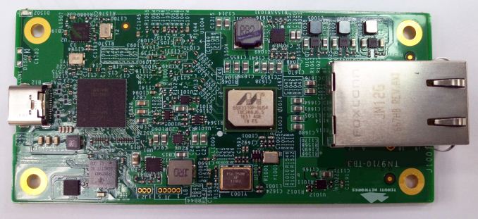
AKiTiO’s Thunder3 10G is now available directly from the company as well as from Amazon for $279.99, which is below MSRP of most Intel-based 10GbE add-on cards. Considering the fact that the latter are generally aimed at servers and high-end workstations (and therefore come with appropriate features and software stack), this is not really surprising. In the meantime, it is noteworthy that the Thunder3 10G costs $120 less than the Thunder2 10G ($399.99), a clear indicator that 10 GbE hardware in general is getting more affordable.
Buy AKiTiO Thunder3 10G on Amazon.com
Related Reading:
- AKiTiO Displays Thunderbolt 3 to 10GBase-T Adapter
- AKiTiO Introduces Node: Thunderbolt 3 eGFX Box for $299
- AKiTiO Thunder3 PCIe SSD Thunderbolt DAS Review
- Thunderbolt 3 in Action: AKiTiO Thunder3 Duo Pro DAS Review
- Lower Cost 10GBase-T Switches Coming: 4, 5 and 8-port Aquantia Solutions at ~$30/Port
- Aquantia Launch AQtion 5G/2.5G/1G Multi-Gigabit Ethernet Cards (NICs) for PCIe
- Aquantia Launches New 2.5G/5G Multi-Gigabit Network Controllers for PCs
More...
-
02-14-18, 12:47 AM #7856
Anandtech: AMD Releases Radeon Software Adrenalin Edition 18.2.2 & Inaugural Ryzen De
This week, AMD released Radeon Software Adrenalin Edition 18.2.2, a smaller patch bringing support for the just-launched Kingdom Come: Deliverance, as well as performance optimizations for Fortnite and PlayerUnknown’s Battlegrounds (PUBG). Purely game-focused, 18.2.2 documents no new bugfixes or issues. And alongside Monday’s launch of AMD Ryzen 5 2400G and Ryzen 3 2200G, AMD has put out the inaugural Windows 10 WHQL drivers specific to those two new APUs.
Released just yesterday, Kingdom Come: Deliverance is a CryEngine-powered first-person single player historical RPG, thematically reminiscent of Mount and Blade and The Witcher. The developers, Warhorse Studios, have stated their desire to focus on realism, story, open-world freedom, and hardcore combat mechanics, the latter of which is not too surprising considering the Operation Flashpoint and ARMA pedigree of Warhorse Studio’s team members.
For Kingdom Come: Deliverance, AMD cites their 18.2.2 testing to show up to 3% faster 1440p performance for the Radeon RX Vega 56 and up to 4% faster 1080p performance for the Radeon RX 580 compared to Radeon Software Adrenalin Edition 18.2.1. As it so happens, Warhorse Studios marks down the Radeon RX 580 as the recommended AMD GPU requirement, with the Radeon HD 7870 as the minimum.
As for Fortnite and PUBG, AMD compares Radeon Software Adrenalin Edition 17.12.1 performance to 18.2.2, claiming 1440p improvements for the Radeon RX Vega 56 up to 3% faster for Fortnite and up to 5% faster for PUBG. Meanwhile, for the Radeon RX 580 at 1080p, AMD cites up to 6% faster performance in Fortnite and up to 7% faster performance in PUBG.
Wrapping things up on the 18.2.2 side, there has been no documented bugfixes and the list of open issues remain identical to 18.2.1:
- FreeSync intermittently engages during Chrome video playback incorrectly, resulting in playback flicker.
- Radeon Overlay hotkey fails to bring up the overlay or causes a Radeon Host Application crash intermittently on a limited number of gaming titles.
- FreeSync may rapidly change between min and max range when enabled causing stutter in fullscreen games on multi display system configurations.
- When Enhanced Sync is enabled on some FreeSync connected displays, flickering occurs with the performance metrics overlay.
- Water textures appear to be missing in World of Final Fantasy.
- A random system hang may be experienced after extended periods of use on system configurations using 12 GPU's for compute workloads.
- The GPU Workload feature may cause a system hang when switching to Compute while CrossFire is enabled. A workaround is to disable CrossFire before switching the toggle to Compute workloads.
Buy AMD Ryzen 5 2400G APU on Amazon.com
Radeon Software for New Ryzen Desktop APUs
Released as “Radeon Software for Ryzen Desktop Processors with Radeon Vega Graphics,” the inaugural public graphics drivers are WHQL certified and are documented as version 17.40.3701 (Windows Driver Store Version 23.20.827.0). The update applies only to the Ryzen 5 2400G and Ryzen 3 2200G, and notes the following:
- RAID drivers are not included in display driver packages. Users wishing to use RAID should navigate to the amd.com APU chipset driver page to find and install RAID drivers.
- AMD has noted a potential system crash while running certain OpenCL applications like Linpack-DGEMM & Indigo benchmark. AMD is currently testing a solution to this issue and an updated driver will be released very shortly. Please visit amd.com for updates.
- 3DMark Firestrike may experience an application hang during GT2 test.
Additionally, AMD has put up a support page for issues with system boot-up failure on configurations with some 2nd generation Ryzen desktop processors (CPUs & APUs) and AM4 motherboards. Unsurprisingly, AMD notes that the likely cause in this scenario is a motherboard that has not been updated to the latest BIOS with APU support, but offers a boot kit solution under warranty if this is not the root cause.
Buy AMD Ryzen 3 2200G APU on Amazon.com
The updated drivers for AMD’s desktop, mobile, and integrated GPUs are available through the Radeon Settings tab or online at the AMD driver download page. More information on these updates and further issues can be found in the respective Radeon Software Adrenalin Edition 18.2.2 release notes and Radeon Software for Ryzen Desktop Processors with Radeon Vega Graphics release notes.
More...
-
02-14-18, 12:58 PM #7857
Anandtech: The Latest High-Capacity M.2: The Samsung 860 EVO 2TB SSD, Reviewed
The Samsung 860 EVO is the mainstream side of Samsung's new generation of consumer SATA SSDs, though our 2TB M.2 drive is a bit of a niche product. Like the 860 PRO, the new 860 EVO provides the necessary improvements to keep up with today's competition, but Samsung is still setting prices like they're the only ones with a high-performance TLC drive.
More...
-
02-14-18, 01:59 PM #7858
Anandtech: Intel Adds Mobile Core i3-8130U to Lineup: Increased Cache and Turbo
Intel on Tuesday introduced the Core i3-8130U, its first mobile 8th Generation Core i3 processor. The new chip features two cores operating at a high frequency and supports Turbo Boost 2.0 technology to make them even faster when power and temperatures permit. The CPU also gains an L3 cache size increase over its predecessors, stepping up to 2MB of inclusive L3 cache per core. However, the new processor is listed as only $16 cheaper than one above it in Intel's stack, the quad-core Core i5-8250U, posing questions about its appeal to the end-user.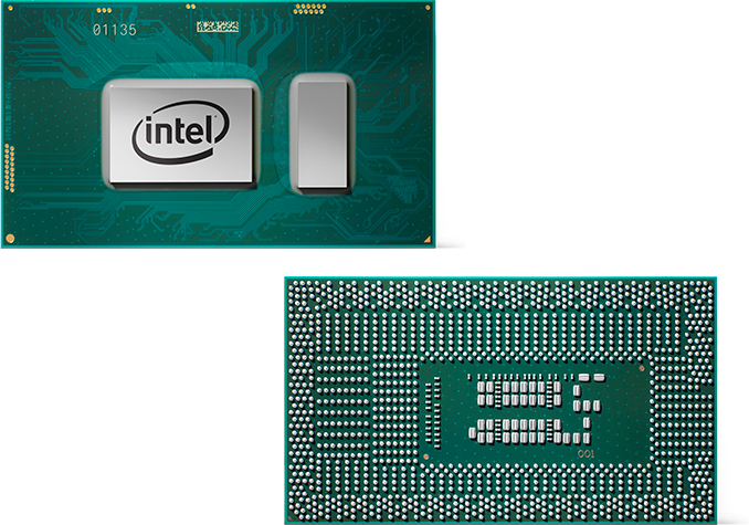
The Core i3-8130U
The Intel Core i3-8130U has two cores with Hyper-Threading, operating at 2.2 GHz base frequency and speeding up to 3.4 GHz in Turbo Boost 2.0 mode; the chip is outfitted with 4 MB of L3 cache and has a 15 W TDP. Previous-generation mobile ULV Core i3 processors came with 3 MB of L3 cache and did not feature Turbo mode, by comparison. The addition of Turbo comes at a different cost, as it would appear that Intel has reduced the base frequency to compensate: the default frequency of the previous generation Core i3-7130U was 2.7 GHz, whereas the new Core i3-8130 is at 2.2 GHz. There is also the added complication that Turbo frequency boosting depends on multiple factors, such as chassis design and cooling performance.
When it comes to graphics and memory, the new CPU features the UHD Graphics 620 iGPU (GT2) as well as a dual-channel memory controller supporting LPDDR3-2133 or DDR4-2400. From silicon point of view, we are dealing with a Kaby Lake Refresh 2+2 design, and the main difference with the original Kaby Lake is the addition of native support of HDMI 2.0, HDCP 2.2, and possible minor fixes.
Intel positions the Core i3-8130U as its lowest-cost offering for the latest mainstream notebooks and 2-in-1 PCs. The processor is listed at $281 in 1000-unit quantities, which is only $16 cheaper than the price of the quad-core Core i5-8250U. Historically, RCPs of Intel’s higher-end mobile Core i3 products have matched (or almost matched) prices of the company’s entry mobile Core i5 offerings, so there is nothing new here.Intel Mobile Core i3 and Core i5 Processors Core i5-8250U Core i3-8130U Core i3-7130U CPU Cores/Threads 4/8 2/4 Frequency Base 1.6 GHz 2.2 GHz 2.7 GHz Dual-Core Turbo ? 3.4 GHz 2.7 GHz Single-Core Turbo 3.4 GHz 3.4 GHz 2.7 GHz TDP (PL1) @ Base Frequency 15 W Instantaneous Turbo Power (PL2) 44 W ? 19 W Configurable TDP-up Freq. 1.8 GHz - - Configurable TDP-up 25 W - - L3 Cache 6 MB 4 MB 3 MB Graphics GPU UHD 620 HD 620 EUs 24 EUs Base Freq. 300 MHz Turbo Freq. 1.1 GHz 1 GHz DRAM Support LPDDR3-2133
DDR4-2400
128-bitDDR3L-1600
LPDDR3-1866
DDR4-2133
128-bitPrice at Launch $297 $281 $281 Launch Timeframe Q3 2017 Q1 2018 Q2 2017
However, the difference between 7th Generation mobile Core i3 and Core i5 was negligible and pricing of these CPUs just reflected that. By contrast, today we are dealing with a $297 quad-core Core i5-8250U operating at 1.6-3.4 GHz as well as a $281 dual-core Core i3-8130U operating at 2.2-3.4 GHz. Despite the clock speed difference, we would expect many modern workloads that are multi-threaded to give the i5-8250U a significant advantage over the i3-8130U. In any case, at $281, the new CPU is currently the most affordable 8th Generation mobile Core processor and it will enable PC makers to build slightly cheaper versions of their latest laptops or 2-in-1s.
Note: The image above depicts Intel’s 8th Generation Core i7 SoC. The 8th Generation Core i3 SoC may look differently.
Related Reading- Intel Launches 8th Generation Core CPUs, Starting with Kaby Lake Refresh for 15W Mobile
- Intel 8th Generation and 9th Generation Processor Lists Leaked: Coffee Lake Refresh?
More...
-
02-15-18, 06:41 AM #7859
Anandtech: Google Announces Cloud TPU v2 Beta Availability for Google Cloud Platform
This week, Google announced Cloud TPU beta availability on the Google Cloud Platform (GCP), accessible through their Compute Engine infrastructure-as-a-service. Using the second generation of Google’s tensor processing units (TPUs), the standard Cloud TPU configuration remains four custom ASICs and 64 GB of HBM2 on a single board, intended for accelerating TensorFlow-based machine learning workloads. With a leased Google Compute Engine VM, Cloud TPU resources can be used alongside current Google Cloud Platform CPU and GPU offerings.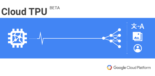
First revealed at Google I/O 2016, the original TPU was a PCIe-based accelerator designed for inference workloads, and for the most part, the TPUv1 was used internally. This past summer, Google announced the inference and training oriented successor, the TPUv2, outlining plans to incorporate it into their cloud services. Both were detailed later at Hot Chips 2017 technical presentations.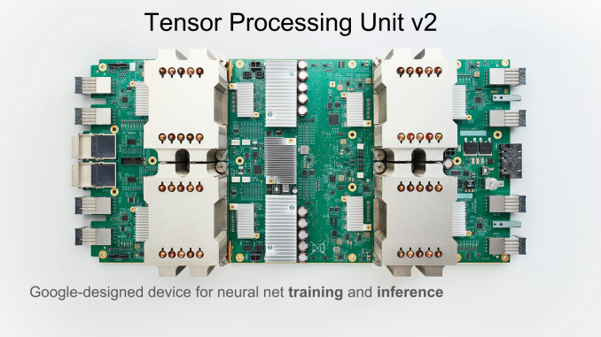
Under the hood, the TPUv2 features a number of changes. Briefly recapping, the second generation TPU ASIC comes with a dual ‘core’ configuration, each having a scalar/vector unit and 128x128 mixed multiply unit capable of 32-bit floating point operations, as opposed to TPUv1’s single core 256x256 MXU and 8-bit integer capability. TPUv2 also improves on the memory bandwidth bottlenecks of its predecessor by using HBM instead of DDR3, with 8GB HBM2 connected to each core for a total of 16 GB per chip.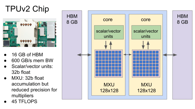
Four of these ASICs form a single Cloud TPU board, ultimately with Google citing up to 180 TFLOPS of unspecified compute performance. As announced earlier, Google is targeting a ‘TPU pod’ setup as one of the end goals, where 64 Cloud TPUs are combined in a dedicated networked array of racks. Google is aiming to offer full TPU Pods on GCP later this year.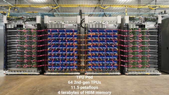
In practical terms, this capability is catered to developers looking for TPU-suitable machine learning performance for particular TensorFlow workloads, with the benefit of Google’s existing cloud infrastructure-as-a-service offerings. Given that it is a beta, Google has a number of documents and tools up on their site. In many ways, the current TPU capabilities exist as a development pipe-cleaner of sorts for the upcoming TPU pods, with Google alluding to the same thing in their announcement. A number of capabilities are yet to be ironed out for TPUs: for example, model parallelism is not yet supported, not all built-in TensorFlow ops are available, and specific limitations exist for training reinforcement learning models, recurrent neural networks (RNN), or generative adversarial networks (GAN).
While select partners have had access to Cloud TPUs for production use, today’s announcement opens the availability to general GCP customers. Google’s Cloud TPUs are available today as purchasable compute time in the US from a Compute Engine provisioned VM, with a $6.50 per TPU per hour rate charged in one-second increments. Interested parties may submit a beta quota request.
Related Reading
More...
-
02-15-18, 09:09 AM #7860
Anandtech: HP Expands DaaS Offerings: Apple Devices, HP VR Solutions, and Tech Café M
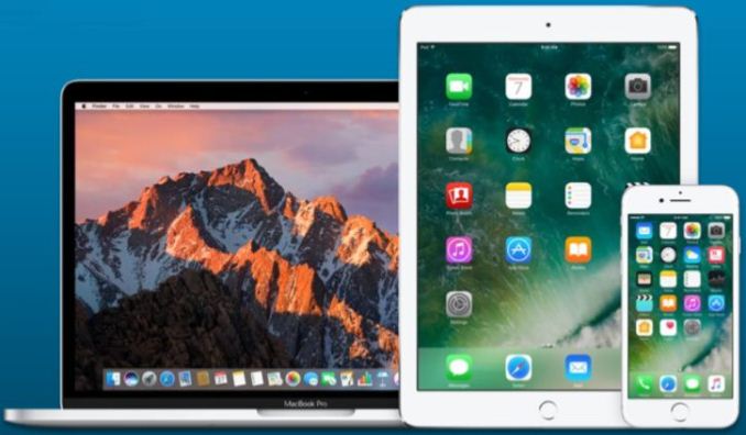
Today, HP announced a new set of Device as a Service (DaaS) offerings for customers and channel partners. Notably, this includes the reveal of DaaS offerings for Apple devices, where HP will provide support for iPhone, iPad, Mac, and other Apple equipment. Along with expansion through Apple products, HP is also expanding their DaaS services to cover their own VR solutions. This includes the Z4 Workstation and the HP Windows Mixed Reality VR headset. HP aims to cover major customer pain points by unifying diverse fleets of different device types and OSes and free up IT resources.
HP DaaS program for Apple will cover dozens of SKU and include multiple versions of each device. Apple coverage includes accidental damage protection as well as next day onsite repair or replacement which can minimize downtime for the user increasing productivity. Part of this plan includes specialized endpoint management. These HP experts are able to deploy applications, provision Wi-Fi access, and set and enforce security policies taking a load off internal IT resources. They are also able to find and protect data on devices that may have been lost or stolen. HP also offers optional services covering the entire device lifecycle from design and planning, as well as configuration and deployment services.
HP is also expanding its real-time hardware analytics and proactive device management capabilities. The analytics are able to capture data including health monitoring (device to component level), security status reports as well analytics and reports for IT planning. Monitoring points such as CPU and Memory utilization, temperatures, battery and HDD life, Windows BSOD and software errors, and security policy compliance are some of the items which are monitored and analyzed. Some of the data can be used to proactively fix or update devices when a trend is recognized. HP says they have nearly 40 Million devices reporting non-PII (Personally Identifiable Information) into their analytics. HP is able to use this data to be able to spot trends and more quickly resolve issues with data collected from both the client level and the entire ‘data lake’ as HP called it.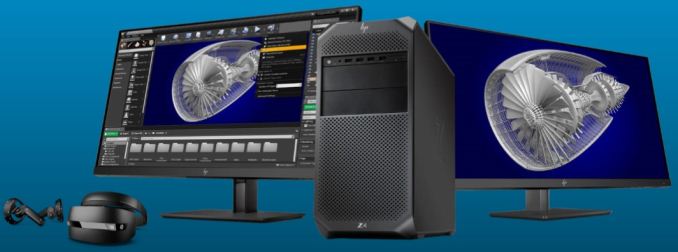
In addition to expanding the available devices and how they are managed, HP also introduced the Tech Cafe Market Enhanced. The Tech Café is an end-to-end smart vending and storage solution able to provide end-users immediate access to accessories and peripherals. A 24/7 locker for device swaps is available for quick exchange of devices for repair or new deployment. End users are able to easily access accessories or new devices directly from the lockers without a dedicated IT resource saving time and improving customer experience. HP can also manage ordering, stock replenishment, and reporting for the clients again with an aim to free up IT resources.
HP’s DaaS update continues to point the service in the direction of a complete end-to-end solution for commercial environments who would like to reduce expenses by essentially renting hardware, while still getting quality IT support for the ever-increasing amount of devices today's workers have. Customers are able to get everything needed from hardware to lifecycle services intended to improve efficiency and free up IT resources. HP’s key value proposition is to deliver a lower total cost of ownership for getting the right product in the user's hands. The rollout for DaaS programs for Apple is in North America now with plans to expand out to India and the Asia-Pacific region in the coming months. Both the new Z4 workstation and the HP Windows Mixed Reality headset is available now.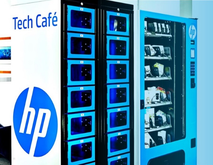
Related Reading:- HP Z4 Workstations Get Xeon W and Core X, 18-Core
- HP Windows Mixed Reality Headset, Professional Edition, Coming March
- HP Announces Updated Elitebook 800 G5 Series and ZBook 14U/15U Laptops
- HP Launches First 4K EliteDisplay and 43-inch 4K Z43
More...


 Quote
QuoteThread Information
Users Browsing this Thread
There are currently 17 users browsing this thread. (0 members and 17 guests)


Bookmarks