

Results 7,971 to 7,980 of 12096
Thread: Anandtech News
-
03-27-18, 06:26 AM #7971
Anandtech: Xiaomi Announces Mi MIX 2S: Snapdragon 845 and Dual Camera for Mi MIX
Today, Xiaomi is announcing its new high mid-range Mi MIX 2S. This is the latest entry in the Mi MIX series, noted for its display that goes all the way to the top of the phone, and one of the first smartphone families to really push the concept of a full-screen display. The 2S succeeds the 6-month old Mi MIX 2 by upgrading the SoC to the latest Qualcomm Snapdragon 845, and upgrading the rear camera to a dual-camera configuration. Support for 7.5W Qi wireless charging and Google ARCore apps are also now part of the device. Xiaomi is also touting some AI functionality in enhanced camera features and smart voice assistant, though technical details were not disclosed.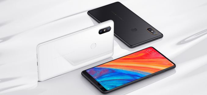
To note, the Mi MIX 2S launch today is for Xiaomi’s current markets, and so does not apply to the US or most of Western Europe. In any case, when asked about the 2S potentially coming to the US, the company only referred back to CEO Lei Jun’s statement earlier this month targeting the end of 2018 to early 2019 timeframe for a general mobile entry into the US market.
Physically-speaking, outside of a smaller top speaker grille and accommodations for the new dual camera, the ceramic-encased design is near identical to the Mi MIX 2, which itself was iterative on the pseudo-concept phone that was the original Mi MIX. The smartphone keeps with the near no-bezel design and larger vertical 18:9 screen, made possible with the same under-display proximity sensor and earpiece speaker at the top and keeping the front camera at the bottom. This last point, of course, means that using the front camera still necessitates flipping the phone upside down unless chins are required.
On the back, the new rear dual camera has been moved to the side as opposed to a symmetrical placement in the middle, matching some other flagship devices. For the overall device specifications, the dual camera is the highlight of the 2S, along with the latest Qualcomm Snapdragon 845 platform, something we’ve just taken a close look at. The 2S brings a new dual 12MP camera configuration, coupled with a number of machine learning based features such as scene detection and dynamic bokeh portrait effects.
With the Snapdragon 845 and Adreno 630, Xiaomi claims a performance increase of up to 30%, as well as a 3x improvement in AI processing due to new on-device functionality on the SD845. While we were provided with a hands-on unit for first impressions, the global ROM remains on an internal build that does not represent final performance of both the SoC as well as the camera and AI featureset. The Chinese product page appears to state that initial batches of the phone will have these AI features enabled with a future MIUI update.Xiaomi Mi MIX 2S SoC Qualcomm Snapdragon 845
4x Kryo 385 Gold @ up to 2.80 GHz
4x Kryo 385 Silver @ up to 1.77 GHz
Adreno 630 @ up to 710 MHzDisplay 5.99-inch 2160x1080 (18:9) Dimensions 150.9 x 74.9 x 8.1 mm
191 gramsRAM 6GB / 8GB LPDDR4x NAND 64GB / 128GB / 256GB Battery 3400 mAh
Qualcomm Quick Charge 3.0
Qi Wireless ChargingFront Camera 5MP, 1.12µm pixels, f/2.0 Primary Rear Camera 12MP, 1.4µm pixels, f/1.8
Sony IMX363Secondary Rear Camera 12MP, 1.0µm pixels, f/2.4
Samsung S5K3M3SIM Size 2x NanoSIM Connectivity 43 global bands (8GB+256GB model only),
4x4 MIMO, 2.4/5G WiFi,
WiFi Direct, WiFi Display,
NFCInterfaces USB 2.0 Type-C Launch OS Android O (8.0) with MIUI 9 Launch Price 6GB/64GB: ¥3299 / $449 / €423
6GB/128GB: ¥3599 / $490 / €462
8GB/256GB: ¥3999 / $544 / €513
The Mi MIX 2S is available for preorders today for the China market, and the Mi MIX 2S will be launching on April 3rd in China (and at a later date for selected global markets). Three configurations in either black or white models will be available, with the price ranging from roughly $449 to $544.
Buy Xiaomi Mi MIX 2 on Amazon.com
Related Reading- Xiaomi Announces Mi 6: 5.15-inch, Snapdragon 835 SoC, 6GB LPDDR4x
- Xiaomi Mi MIX: A Closer Look at the Design and Display
- Performance & Battery Life Report: Xiaomi Redmi Note 4 with MediaTek Helio X20
- Xiaomi Announces the Mi Note 2 (Snapdragon 821, 6GB RAM) and Mi MIX Concept Phones
More...
-
03-27-18, 07:31 AM #7972
Anandtech: Samsung Reveals M.2 Z-SSD
Last week at the Open Compute Project (OCP) Summit in San Jose, Samsung's booth included a surprise appearance of a Z-SSD in the M.2 form factor. Samsung has been pitching their Z-SSD SZ985 using Z-NAND memory as a low-latency competitor to Intel's 3D XPoint-based Optane SSDs. The Z-SSD SZ985 has made many trade show appearances over the course of its development, but always in the form of a half-height half-length PCIe add-in card.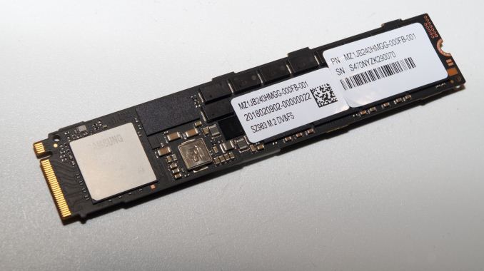
That card keeps all the interesting components covered by a heatsink, leaving us with little indication of the PCB's layout, but some of Samsung's earlier presentations included renderings showing a very large SSD controller, similar in size to a typical 16-channel controller. Samsung's exhibit at the OCP Summit included a M.2 version of the SZ985, revealing that the controller is in fact the same Phoenix 8-channel controller used on Samsung's other 98x SSDs, including the PM981 client SSD. This controller is also very likely to be used in Samsung's next generation consumer retail NVMe SSDs, the successors to the 960 PRO and 960 EVO.
Samsung's exhibit called the drive the SZ985 Z-SSD, but the stickers on the drive say SZ983. The capacity of the demo unit appears to be 240GB, the same as the smaller capacity announced earlier this year when the Z-SSD SZ985 officially launched. Samsung's display also listed a 480GB capacity, likely the most first-generation Z-NAND that Samsung can fit onto the M.2 card.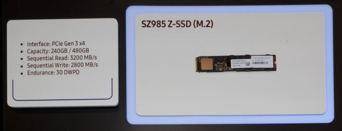
The development of a M.2 Z-SSD raises the possibility of Samsung introducing a Z-SSD for the enthusiast consumer market, to compete against the Intel Optane SSD 800P. However, it is likely that Samsung can remain quite competitive in the high-end consumer SSD space with another conventional MLC-based SSD to replace the 960 PRO. Sacrificing further capacity for incremental performance gains would probably not be worthwhile, even though a Z-SSD doesn't go as far down that road as Optane SSDs.
Gallery: Samsung Reveals M.2 Z-SSD

More...
-
-
03-27-18, 09:59 AM #7974
Anandtech: Huawei P20 and P20 Pro Hands-On: Embrace the Notch
It’s time to have a serious discussion about the Notch. Love it or hate it, the Notch is going to be a defining element of major smartphones this year. The latest adherent to the Notch philosophy is the Huawei P20 family, being announced in Paris today. Using the Notch allows the handset to maximise the front-facing screen size compared to the size of the phone, and if used in the right way is designed not to be a distraction. We had some hands on time with the device, the P20 Pro triple camera setup, the new color schemes, and the new 960 fps mode.
More...
-
03-27-18, 10:36 AM #7975
Anandtech: Acer Announces Chromebook Tab 10: A Tablet Running Googles Chrome OS
This week Acer introduced its first tablet running Chrome OS, a tablet positioned primarily for the education market. Chrome OS runs Android applications from Google Play store and is growing in popularity with convertible PCs, but nothing stops hardware makers form using the OS for tablets.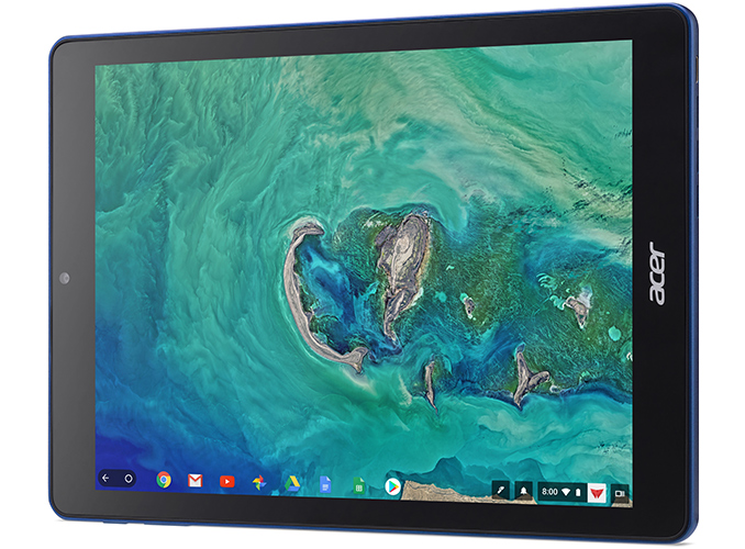
The Acer Chromebook Tab 10 (D651N) is based on the Rockchip OP1 processor which incorporates two high-performance ARM Cortex-A72 cores, four energy-efficient Cortex-A53 cores, supports hardware decode/encoder for UHD 4K video, and has a number of Chrome OS-specific optimizations designed to improve user experience (and brought in by Google). The tablet is equipped with 4 GB of RAM and 32 GB of onboard storage (which can be enhanced with a microSD card), which is in line with other education-oriented Chrome OS-powered devices. When it comes to display, the Chromebook Tab 10 has a fairly standard 9.7-inch touch-enabled LCD with a 2048×1536 resolution at 264 pixels per inch. As for connectivity, the tablet is outfitted with 2×2 802.11ac Wi-Fi as well as Bluetooth 4.1 technologies. In addition, it has a TRRS audio jack as well as USB 3.0 Type-C connector for data, charging, and display connectivity.
Since the Chromebook Tab 10 is designed primarily for educational applications, it comes with a Wacom EMR stylus to take notes and to sketch on. Another interesting capability that will be supported by the device (but not out-of-the-box) is support for Google’s Expeditions AR software that can map classrooms and place 3D objects in it.
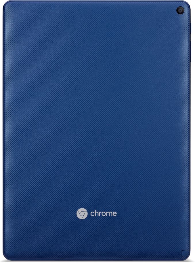
The Chromebook Tab 10 is 9.98 mm (0.39”) thick and weighs 550 grams (1.21 lbs), which is too thick and too heavy by consumer standards, but which is okay for devices that will be stored in classrooms or carried in backpacks. In addition, the tablets will come in cobalt blue plastic enclosures - not necessarily a standard color for a business environment, but easy to find in a classroom.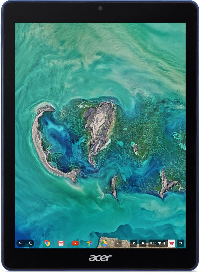
Adopters of Chrome OS position appropriate devices primarily for education market, so it is not surprising that Acer decided to start roll-out of Chrome OS-based tablets with a model for schools. This platform is good enough for education, but it yet has to gain traction among consumers. Meanwhile, no matter how strong Google’s Android is on smartphones, tablet software for this platform is often mediocre at best. In a bid not to leave tablet and convertible form-factors almost entirely to Apple and Microsoft, Google has been working to bring its Chrome OS and Android platforms together for several years now. While it is unlikely that Google will cease to offer Android for tablets, Chrome OS-powered higher-end tablets make a lot of sense since they support productivity enabled by Chrome OS, but can also run educational and entertainment apps for Android. That said, it makes a lot of sense for companies like Acer to start rolling out such devices now starting from SKUs for schools and expanding offerings to general consumers later.The Acer Chromebook Tab 10 D651N Display Diagonal 9.7" Resolution 2048×1536 PD 264 PPI SoC Rockchip OP1
2 × ARM Cortex-A72
4 × ARM Cortex-A53RAM 4 GB Storage 32 GB Wi-Fi 2×2 802.11ac Wi-Fi module Bluetooth BT 4.1 USB 1 × USB Type-C (5 Gbps) for data, charging, display output Other I/O 2 MP webcam, 5MP rear camera,
TRRS connector for audio, speakers, microphoneDimensions (H × W × D) 238.2 mm × 172.2 mm × 9.98 mm
9.38" × 6.78" × 0.39"Weight 550 grams / 1.21 pounds Battery Life 9 hours (34 Wh) Price North America: $329
EMEA: €329
Acer plans to start sales of the Chrombook Tab 10 in North America next month at $329. The device will land in EMEA sometimes in May at €329 (including VAT). The tablet will be initially available to education and commercial customers, who will have plenty of time to test drive the device before deploying it later this year.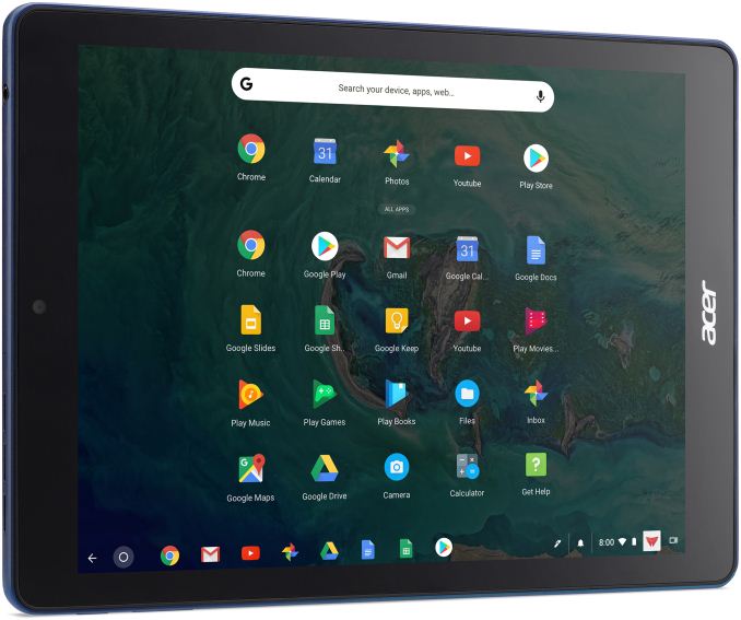
Buy Acer Chromebook 14 (2018) on Amazon.com
Related Reading- New Chrome OS Update Enables Google Play on Acer’s and ASUS' Chromebooks
- Acer Announces New Chromebooks And Chromebox Devices
- Acer Announces The Rugged Chromebook 11 N7: Designed For Education
- Google Launches Pixelbook: 12.3” LCD, Kaby Lake, 16 GB RAM, 512 GB SSD, Assistant, Stylus
More...
-
03-27-18, 12:06 PM #7976
Anandtech: NVIDIA Bumps All Tesla V100 Models to 32GB, Effective Immediately
When first launched last year, the original Tesla V100 shipped with 16GB of HBM2 memory. Now just a little less than a year into its lifetime, NVIDIA is announcing that their workhorse server accelerator is getting a memory capacity bump to 32GB, effectively immediately.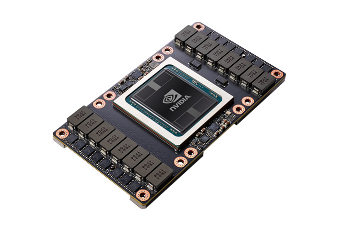
For the last couple of years now, NVIDIA has been relying on 4GB (4-Hi) HBM2 memory stacks for their Tesla P100 and Tesla V100 products, as this was the first HBM2 memory to be ready in reasonable commercial volumes. Now that Samsung and SK Hynix have a better grip on HBM2 manufacturing, 8GB (8Hi) HBM2 stacks are far more readily available and reliable. As a result, the conditions are right for NVIDIA to finally give their Tesla cards a long-awaited memory upgrade.
This upgrade will be across the entire Tesla V100 family – all SKUs for SMX and PCIe cards are getting their memory doubled. The Tesla V100’s specifications otherwise remain identical, with the same GPU and memory clocks along with the same TDPs. We’re also told that the mechanical specifications are identical as well, which would mean that the 8-Hi stacks won’t cause any cooling problems due to changes in memory stack height.
It should be noted that this upgrade is a wholesale replacement of the existing 16GB versions in NVIDIA’s product stack, as NVIDIA won’t be retaining the 16GB versions now that the 32GB versions are out. So all new cards sold by NVIDIA going forward will be the 32GB cards, and OEMs will be making the same transition in Q2 as their 16GB stocks are depleted and replaced with 32GB cards.NVIDIA Tesla/Titan Family Specification Comparison Tesla V100
(SXM2)Tesla V100
(PCIe)Titan V
(PCIe)Tesla P100
(SXM2)CUDA Cores 5120 5120 5120 3584 Tensor Cores 640 640 640 N/A Core Clock ? ? 1200MHz 1328MHz Boost Clock 1455MHz 1370MHz 1455MHz 1480MHz Memory Clock 1.75Gbps HBM2 1.75Gbps HBM2 1.7Gbps HBM2 1.4Gbps HBM2 Memory Bus Width 4096-bit 4096-bit 3072-bit 4096-bit Memory Bandwidth 900GB/sec 900GB/sec 653GB/sec 720GB/sec VRAM 16GB
32GB16GB
32GB12GB 16GB L2 Cache 6MB 6MB 4.5MB 4MB Half Precision 30 TFLOPS 28 TFLOPS 27.6 TFLOPS 21.2 TFLOPS Single Precision 15 TFLOPS 14 TFLOPS 13.8 TFLOPS 10.6 TFLOPS Double Precision 7.5 TFLOPS 7 TFLOPS 6.9 TFLOPS 5.3 TFLOPS Tensor Performance
(Deep Learning)120 TFLOPS 112 TFLOPS 110 TFLOPS N/A GPU GV100 GV100 GV100 GP100 Transistor Count 21B 21B 21.1B 15.3B TDP 300W 250W 250W 300W Form Factor Mezzanine (SXM2) PCIe PCIe Mezzanine (SXM2) Cooling Passive Passive Active Passive Manufacturing Process TSMC 12nm FFN TSMC 12nm FFN TSMC 12nm FFN TSMC 16nm FinFET Architecture Volta Volta Volta Pascal
NVIDIA’s Tesla V100-equipped systems will also be getting the same upgrade. Both the DGX-1 server and DGX Station will now ship with the 32GB cards. And while OEMs are a bit farther behind, ultimately I expect they’ll make the same move since the 16GB cards are going away anyhow. Meanwhile NVIDIA isn’t officially talking about pricing here for either the new V100 cards or the updated DGX systems. However as the new parts are essentially drop-in replacements in their respective ongoing lines, there aren’t any signs right now that pricing is changing.
As far as workloads go, since the specifications of the Tesla V100 aren’t changing outside of memory capacity, the benefit and performance impact of this upgrade is almost entirely rooted in dataset size. Workloads that rely on datasets that couldn’t previously fit entirely within a Tesla V100 card should see a sizable boost, as will any applications that can benefit from more local memory for caching purposes. However in pure compute-bound scenarios, the new cards shouldn’t perform any differently than the outgoing models.
Meanwhile, as for NVIDIA's workstation-oriented Titan V, nothing is being announced at this time. The 12GB card could easily be bumped to 24GB using the 8-Hi stacks, however it's not clear if NVIDIA is in a hurry to do so. In practice it will almost certainly come down to whether NVIDIA wants to keep GV100 GPU production to a single line for efficiency reasons, or if they'll operate two lines as part of a broader product segmentation strategy.
Lastly, this upgrade means that NVIDIA has finally caught up with arch-rival AMD in total memory capacity. AMD has been shipping a 32GB FirePro S9170 card using 16x2GB GDDR5 modules for the better part of the last 3 years now, a mark that NVIDIA couldn’t catch up to until 8-Hi HBM2 was ready. The Tesla V100 has always been significantly more powerful than the W9100 regardless, but this finally brings NVIDIA to parity in the one area where they were trailing AMD in the server space.
More...
-
03-27-18, 12:06 PM #7977
Anandtech: GIGABYTE's G190-G30: a 1U Server with Four Volta and NVLink
GIGABYTE Server, the B2B arm of GIGABYTE's enterprise line, is adding the G190-G30 to its roster. This is a 1U server that uses four SXM2 GPUs and dual Xeon CPUs. This GPU form factor is designed for embedded on-board connectivity, similar to NVIDIA's DGX-1 server line. The G190-G30 is designed to accommodate four NVIDIA Tesla V100 or P100 GPU accelerators, using NVLink for higher bandwidth and improved scalability over PCIe for the GPU to GPU interconnects. This design is said to allow increased flexibility and performance throughout the lineup.
Using the NVIDIA Tesla V100 in the G190-G30, the system is able to support up to six NVLink links, each with a signaling rate of 25 GB/s in each direction, for a total bandwidth of 300 GB/s or 10x the bandwidth of PCIe. The higher bandwidth and reduced latency of the cards should allow servers that use them to remove interconnectivity bottlenecks and achieve better performance in intensive cross-communicative computing applications. The P100 Pascal based GPUs use four NVLinks at 20 GB/s in each direction.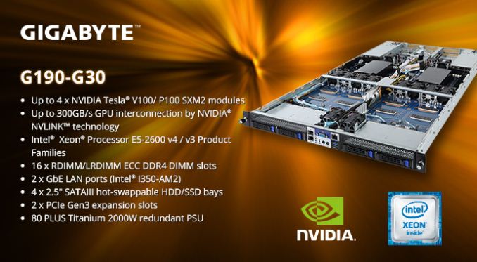
Internally, the H190-G30 supports dual Intel Xeon Processors in the E5-2600 v4/v3 product families (Broadwell and Haswell). This means up to dual 22 core processors. Each CPU has a total of eight RDIMM/LRDIMM ECC DDR4 DIMM slots in quad channel, supporting up to 1TB when fully populated with 64GB DIMMs and v4 CPUs. The server also uses dual Intel I350-AM2 GbE LAN ports, four 2.5-inch SATA3 hot-swappable HDD/SSD bays and has two low-profile half-length PCIe 3.0 x16 slots (at 3.0 x8). GIGBYTE’s optimized airflow comes from 10 40x56mm dual rotor fans and four 40x56mm single rotor fans. Powering the entire server are dual 2000W redundant PSUs sporting an 80 Plus Titanium rating.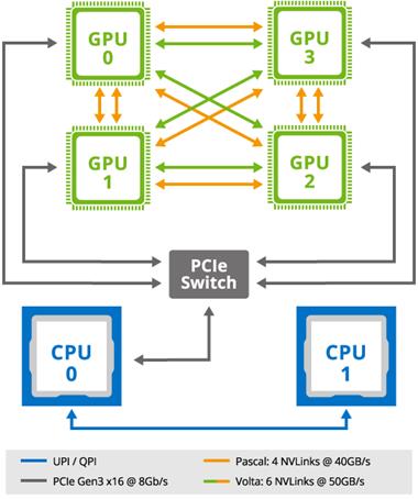
Interested customers will need to get in contact with their local GIGABYTE Server representatives for more information.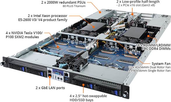
Buy NVIDIA Titan V 12GB on Amazon.com
Related Reading:- GIGABYTE Server Launches Three New Density-Focused Servers: Skylake-SP, Choice of NIC
- Immersion Server Liquid Cooling: ZTE makes a Splash at MWC
- More EPYC Servers: Dell Launches 1P and 2P PowerEdge for HPC and Virtualization
- Sizing UP Servers: Intel's Skylake-SP Xeon versus AMD's EPYC 7000 - The Sever CPU Battle of the Decade?
- Intel to Update Xeon D in Early 2018, with Skylake-SP Cores
- Intel Launches Xeon-W CPUs for Workstations: Skylake-SP & ECC for LGA2066
More...
-
03-27-18, 12:51 PM #7978
Anandtech: Big Volta Comes to Quadro: NVIDIA Announces Quadro GV100
Along with today’s memory capacity bump for the existing Tesla V100 cards, NVIDIA is also rolling out a new Volta-based card for the Quadro family. Aptly named the Quadro GV100, this is the successor to last year’s Quadro GP100, and marks the introduction of the Volta architecture into the Quadro family.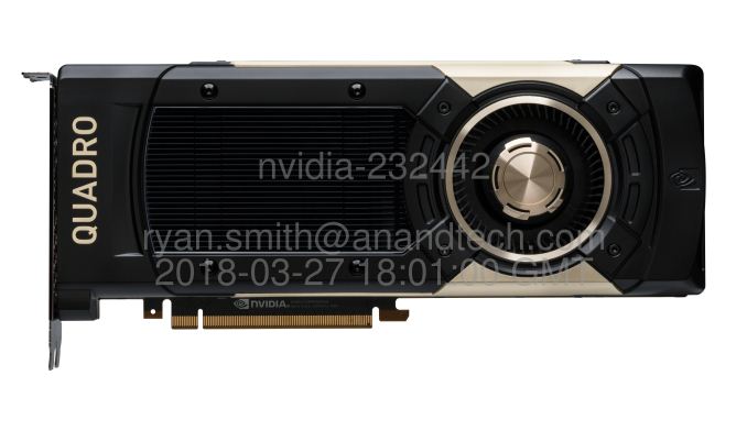
As a consequence of NVIDIA’s GPU lines bifurcating between graphics and compute, in the last couple of years the Quadro family has been in an odd spot where it straddles the line between the two. Previously the king of all NVIDIA cards, instead the Quadro family itself has been bifurcated a bit, between the compute GPU-derrived cards like the Quadro GP100 and now GV100, and the more pure graphics cards like the P-series. The introduction of the Quadro GV100 in turn looks to maintain status quo here, delivering an even more powerful Quadro card with chart-topping graphics performance, but also the GV100’s GPU’s strong compute heritage.
While NVIDIA’s pre-brief announcement doesn’t mention whether the Quadro GP100 is being discontinued, the Quadro GV100 is none the less the de facto replacement for NVIDIA’s last current-generation Big Pascal card. The official specifications for the card put it at 14.8 TFLOPs of single precision performance, which works out to a fully-enabled GV100 GPU clocked at around 1.45GHz. This is only a hair below the mezzanine Tesla V100, and ahead of the PCIe variant. And like the capacity-bumped Tesla cards, the Quadro GV100 ships with 32GB of natively ECC-protected HBM2. This finally gets an NVIDIA professional visualization card to 32GB; the GP100 was limited to 16GB, and the Quadro P6000 tops out at 24GB.NVIDIA Quadro Specification Comparison GV100 GP100 P6000 M6000 CUDA Cores 5120 3584 3840 3072 Tensor Cores 640 N/A N/A N/A Texture Units 320 224 240 192 ROPs 128 128 96 96 Boost Clock ~1450MHz ~1430MHz ~1560MHz ~1140MHz Memory Clock 1.7Gbps HBM2 1.4Gbps HBM2 9Gbps GDDR5X 6.6Gbps GDDR5 Memory Bus Width 4096-bit 4096-bit 384-bit 384-bit VRAM 32GB 16GB 24GB 24GB ECC Full Full Partial Partial Half Precision 29.6 TFLOPs? 21.5 TFLOPs N/A N/A Single Precision 14.8 TFLOPs 10.3 TFLOPs 12 TFLOPs 7 TFLOPs Double Precision 7.4 TFLOPs 5.2 TFLOPs 0.38 TFLOPs 0.22 TFLOPs Tensor Performance 118.5 TLFOPs N/A N/A N/A TDP 250W 235W 250W 250W GPU GV100 GP100 GP102 GM200 Architecture Volta Pascal Pascal Maxwell 2 Manufacturing Process TSMC 12nm FFN TSMC 16nm TSMC 16nm TSMC 28nm Launch Date March 2018 March 2017 October 2016 March 2016
On the features front, the card also ships with NVIDIA’s tensor cores fully enabled, with performance again in the ballpark of the Tesla V100. Like the Quadro GP100’s compute features, the tensor cores aren’t expected to be applicable to all situations, but there are some professional visualization scenarios where NVIDIA expects it to be of value. More importantly though, the Quadro GV100 continues the new tradition of shipping with 2 NVLink connectors, meaning a pair of the cards can be installed in a system and enjoy the full benefits of the interface, particularly low latency data transfers, remote memory access, and memory pooling.
At a high level, the Quadro GV100 should easily be the fastest Quadro card, a distinction the GP100 didn’t always hold versus its pure graphics siblings, and that alone will undoubtedly move cards. As we’ve already seen with the Titan V in the prosumer space – NVIDIA dodging expectations by releasing the prosumer Volta card first and ProViz card second – the Titan V can be a good deal faster than any of the Pascal cards assuming that software is either designed to take advantage of the architecture, or at least meshes well with NVIDIA’s architectural upgrades. Among other things, NVIDIA is once again big into virtual reality this year, so the GV100 just became their flagship VR card, a convenient timing for anyone looking for a fast card to drive the just-launched HTC Vive Pro.
However the GV100’s bigger calling within NVIDIA’s ecosystem is that it’s now the only Quadro card using the Volta architecture, meaning it’s the only card to support hardware raytracing acceleration, vis a vie NVIDIA’s RTX technology. Announced last week at the 2018 Game Developers Conference, RTX is NVIDIA’s somewhat ill-defined hardware acceleration backend for real-time raytracing. And while the GDC announcement was focused on the technology’s use in games and game development, at GTC the company is focusing on the professional uses of it, including yet more game development, but also professional media creation. Not that NVIDIA expects movie producers to sudden do final production in real-time on GPUs, but as with the game asset creation scenario, the idea is to significantly improve realism during pre-production by giving artists a better idea of what a final scene would look like.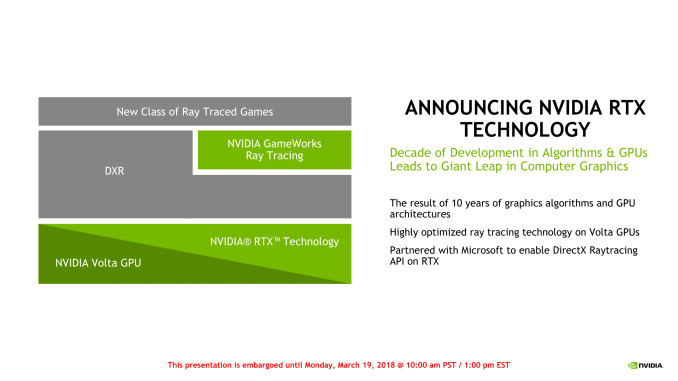
Along with Microsoft’s new DirectX Raytracing API, the RTX hardware will also be available within NVIDIA’s OptiX ray tracing engine – which is almost certainly a better fit for ProViz users – while NVIDIA is also saying that Vulkan support is on tap for the future. And like the game development scenario, NVIDIA will also be looking to leverage their tensor cores here as well in order to use them for AI denoising. Which, given the still limited raytracing performance of current hardware, is increasingly being setup as the critical component for making real-time ray tracing viable in 2018.
Otherwise, the Quadro GV100 looks to be a fairly standard Quadro card. TDP has gone up ever slightly from the Quadro GP100 – from 235W to 250W – so while it should generally be drop-in replaceable, it’s not strictly identical. Nor are the display outputs identical; the Quadro GV100 has dropped the GP100’s sole DVI port, leaving it with a pure 4x DisplayPort 1.4 setup. The card also features the standard Quadro Sync and Stereo connectors for synchronized refresh and quad-buffered stereo respectively.
Wrapping things up, the Quadro GV100 is shipping immediately from NVIDIA, and OEMs will begin including it in their systems in June. Official pricing has not been announced, but like the GP100 before it, I would expect this card to run for north of $5,000.
More...
-
03-27-18, 12:51 PM #7979
Anandtech: NVIDIA Develops NVLink Switch: NVSwitch, 18 Ports For DGX-2 & More
Back in 2016 when NVIDIA launched the Pascal GP100 GPU and associated Tesla cards, one of the consequences of their increased server focus for Pascal was that interconnect bandwidth and latency became an issue. Having long relied on PCI Express, NVIDIA’s goals for their platform began outpacing what PCIe could provide in terms of raw bandwidth, never mind ancillary issues like latency and cache coherency. As a result, for their compute focused GPUs, NVIDIA introduced a new interconnect, NVLink.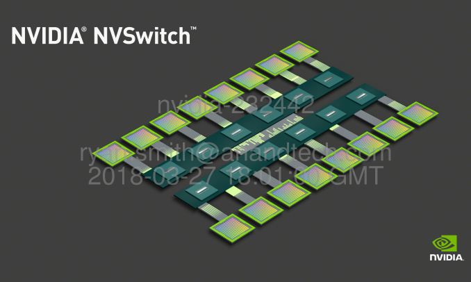
With 4 (and later 6) NVLinks per GPU, these links could be teamed together for greater bandwidth between individual GPUs, or lesser bandwidth but still direct connections to a greater number of GPUs. In practice this limited the size of a single NVLink cluster to 8 GPUs in what NVIDIA calls a Hybrid Mesh Cube configuration, and even then it’s a NUMA setup where not every GPU could see every other GPU. Past that, if you wanted a cluster larger than 8 GPUs, you’d need to resort to multiple systems connected via InfiniBand or such, losing some of the shared memory and latency benefits of NVLink and closely connected GPUs.
For practical reasons, going with an even larger number of NVLInks on a single GPU is increasingly impractical. So instead NVIDIA is doing the next best thing – and taking the next step as an interconnect vendor – by producing an NVLink switch chip.
8x Tesla V100s in a Hybrid Mesh Cube Topology
The switch, aptly named NVSwitch, is designed to enable clusters of much larger GPUs by routing GPUs through one or more switches. A single switch has a whopping 18 full-bandwidth ports – three-times that of a GV100 GPU – with all of the ports in a fully connected crossbar. As a result a single switch has an aggregate of 900GB/sec of bidirectional bandwidth.
The immediate goal with NVSwitch is to double the number of GPUs that can be in a cluster, with the switch easily allowing for a 16 GPU configuration. But more broadly, NVIDIA wants to take NVLink lane limits out of the equation entirely, as through the use of multiple switches it should be possible to build almost any kind of GPU topology. Consequently the NVSwitch is something of a “spare no expense” project for the company; this is embodied by the transistor count of the chip, which weighs in at around 2 billion transistors. This makes it larger than even NVIDIA’s entry-level GP108 GPU, and considering this is just for a switch, all of this amounts to somewhat crazy number of transistors.
Unfortunately while NVIDIA has announced the bandwidth numbers for the NVSwitch, they aren’t yet talking about latency. The introduction of a switch will unquestionably add latency, so it will be interesting to see just what the penalty is like. Staying on-system (and with short traces) means it should be low, but it would diminish the latency advantages of NVLink somewhat. Nor for that matter have power consumption or pricing been announced.
DGX-2: 16 Tesla V100s In a Single System
Unsurprisingly, the first system to ship with the NVSwitch will be a new NVIDIA system: the DGX-2. The big sibling to NVIDIA’s existing DGX-1 system, the DGX-2 incorporates 16 Tesla V100 GPUs. Which as NVIDIA likes to tout, means it offers a total of 2 PFLOPs of compute performance in a single system, albeit via the more use-case constrained tensor cores.
NVIDIA hasn’t published a complete diagram of the DGX-2’s topology yet, but the high level concept photo provided indicates that there are actually 12 NVSwitches (216 ports) in the system in order to maximize the amount of bandwidth available between the GPUs. With 6 ports per Tesla V100 GPU, this means that the Teslas alone would be taking up 96 of those ports if NVIDIA has them fully wired up to maximize individual GPU bandwidth within the topology.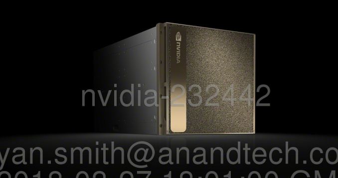
Notably here, the topology of the DGX-2 means that all 16 GPUs are able to pool their memory into a unified memory space, though with the usual tradeoffs involved if going off-chip. Not unlike the Tesla V100 memory capacity increase then, one of NVIDIA’s goals here is to build a system that can keep in-memory workloads that would be too large for an 8 GPU cluster. Providing one such example, NVIDIA is saying that the DGX-2 is able to complete the training process for FAIRSeq – a neural network model for language translation – 10x faster than a DGX-1 system, bringing it down to less than two days total.
Otherwise, similar to its DGX-1 counterpart, the DGX-2 is designed to be a powerful server in its own right. We’re still waiting on the final specifications, but NVIDIA has already told us that it’s based around a pair of Xeon Platinum CPUs, which in turn can be paired with up to 1.5TB of RAM. On the storage side the DGX-2 comes with 30TB of NVMe-based solid state storage, which can be further expanded to 60TB. And for clustering or further inter-system communications, it also offers InfiniBand and 100GigE connectivity.
Ultimately the DGX-2 is being pitched at an even higher-end segment of the deep-learning market than the DGX-1 is. Pricing for the system has not yet been announced, but if you can afford it (and can justify the cost) you’re probably Facebook or Google.NVIDIA DGX-2 Specifications CPUs 2x Intel Xeon Platinum (Skylake-SP) GPUs 16x NVIDIA Tesla V100 System Memory Up To 1.5 TB DDR4 (LRDIMM) GPU Memory 512GB HBM2 (16x 32GB) Storage 30TB NVMe, Upgradable to 60TB Networking Infiniband + 100GigE Power [All of it] Size ? GPU Throughput FP16: 480 TFLOPs
FP32: 240 TFLOPs
FP64: 120 TFLOPs
Tensor (Deep Learning): 1.92 PFLOPs
More...
-
03-27-18, 02:11 PM #7980
Anandtech: NVIDIAs DGX-2: Sixteen V100 GPUs, 30 TB of NVMe, only $400K
Ever wondered why the consumer GPU market is not getting much love from NVIDIA’s Volta architecture yet? This is a minefield of a question, nuanced by many different viewpoints and angles – even asking the question will poke the proverbial hornet nest inside my own mind of different possibilities. Here is one angle to consider: NVIDIA is currently loving the data center, and the deep learning market, and making money hand-over-fist. The Volta architecture, with CUDA Tensor cores, is unleashing high performance to these markets, and the customers are willing to pay for it. So introduce the latest monster from NVIDIA: the DGX-2.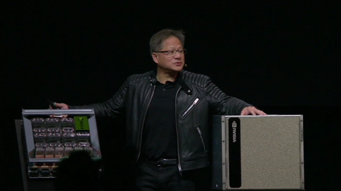
DGX-2 builds upon DGX-1 in several ways. Firstly, it introduces NVIDIA’s new NVSwitch, enabling 300 GB/s chip-to-chip communication at 12 times the speed of PCIe. This, with NVLink2, enables sixteen GPUs to be grouped together in a single system, for a total bandwidth going beyond 14 TB/s. Add in a pair of Xeon CPUs, 1.5 TB of memory, and 30 TB of NVMe storage, and we get a system that consumes 10 kW, weighs 350 lbs, but offers easily double the performance of the DGX-1. NVIDIA likes to tout that this means it offers a total of ~2 PFLOPs of compute performance in a single system, when using the tensor cores.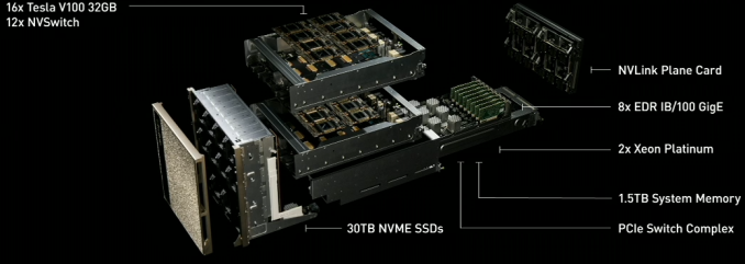
NVIDIA’s overall topology relies on a dual stacked system. The high level concept photo provided indicates that there are actually 12 NVSwitches (216 ports) in the system in order to maximize the amount of bandwidth available between the GPUs. With 6 ports per Tesla V100 GPU, each running in the larger 32GB of HBM2 configuration, this means that the Teslas alone would be taking up 96 of those ports if NVIDIA has them fully wired up to maximize individual GPU bandwidth within the topology.NVIDIA DGX Series (with Volta) DGX-2 DGX-1 CPUs 2 x Intel Xeon
Platinum2 x Intel Xeon
E5-2600 v4GPUs 16 x NVIDIA Tesla V100
32GB HBM28 x NVIDIA Tesla V100
16 GB HBM2System Memory Up to 1.5 TB DDR4 Up to 0.5 TB DDR4 GPU Memory 512 GB HBM2
(16 x 32 GB)128 GB HBM
(8 x 16 GB)Storage 30 TB NVMe
Up to 60 TB4 x 1.92 TB NVMe Networking 8 x Infiniband or
8 x 100 GbE4 x IB +
2 x 10 GbEPower 10 kW 3.5 kW Size 350 lbs 134 lbs GPU Throughput Tensor: 1920 TFLOPs
FP16: 480 TFLOPs
FP32: 240 TFLOPs
FP64: 120 TFLOPsTensor: 960 TFLOPs
FP16: 240 TFLOPs
FP32: 120 TFLOPs
FP64: 60 TFLOPsCost $399,000 $149,000
Notably here, the topology of the DGX-2 means that all 16 GPUs are able to pool their memory into a unified memory space, though with the usual tradeoffs involved if going off-chip. Not unlike the Tesla V100 memory capacity increase then, one of NVIDIA’s goals here is to build a system that can keep in-memory workloads that would be too large for an 8 GPU cluster. Providing one such example, NVIDIA is saying that the DGX-2 is able to complete the training process for FAIRSEQ – a neural network model for language translation – 10x faster than a DGX-1 system, bringing it down to less than two days total rather than 15.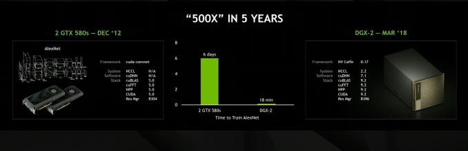
AlexNET, the network that 'started' the latest machine learning revolution, now takes 18 minutes
Otherwise, similar to its DGX-1 counterpart, the DGX-2 is designed to be a powerful server in its own right. Exact specifications are still TBD, but NVIDIA has already told us that it’s based around a pair of Xeon Platinum CPUs, which in turn can be paired with up to 1.5TB of RAM. On the storage side the DGX-2 comes with 30TB of NVMe-based solid state storage, which can be further expanded to 60TB. And for clustering or further inter-system communications, it also offers InfiniBand and 100GigE connectivity, up to eight of them.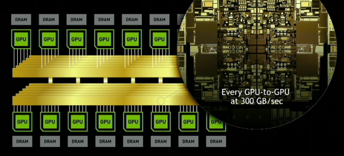
The new NVSwitches means that the PCIe lanes of the CPUs can be redirected elsewhere, most notably towards storage and networking connectivity.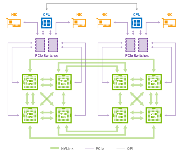
Ultimately the DGX-2 is being pitched at an even higher-end segment of the deep-learning market than the DGX-1 is. Pricing for the system runs at $400k, rather than the $150k for the original DGX-1. For more than double the money, the user gets Xeon Platinums (rather than v4), double the V100 GPUs each with double the HBM2, triple the DRAM, and 15x the NVMe storage by default.
NVIDIA has stated that DGX-2 is already certified for the major cloud providers.
Related Reading- Big Volta Comes to Quadro: NVIDIA Announces Quadro GV100
- The NVIDIA GTC 2018 Keynote Live Blog
- NVIDIA Develops NVLink Switch: NVSwitch, 18 Ports For DGX-2 & More
- NVIDIA Volta Unveiled: GV100 GPU and Tesla V100 Accelerator Announced
- NVIDIA Ships First Volta-based DGX Systems
- NVIDIA Unveils the DGX-1 HPC Server: 8 Teslas, 3U, Q2 2016
More...


 Quote
QuoteThread Information
Users Browsing this Thread
There are currently 15 users browsing this thread. (0 members and 15 guests)


Bookmarks