

Results 8,051 to 8,060 of 12096
Thread: Anandtech News
-
04-19-18, 04:07 PM #8051
Anandtech: Motorola Announces Moto g6 and e5
Today Motorola announced six new mid-range and low-end phones in the g6 and e5 series. The G series has been particularly popular in regions such as North America due to its excellent value proposition and being overall solid phones. The g6 promises to continue this trend while bringing to market some of the more popular features of today’s high-end flagships, such as 18:9 displays and dual-camera functionality.
The new g6 and e5 series each come in three variants: A regular variant in a “smaller” form-factor, a “plus” variant with a larger screen which will be available only in select markets, and a cost-reduced and “play” variant which could be counted as a completely different phone model with low-end specifications.
The g6 and g6 plus are powered by a Snapdragon 430 which uses 8x Cortex A53 at up to 1.4GHz, so this is a low-end device in terms of specifications and performance. The g6 and g6 plus come with respectively 3/4 or 4/6GB or RAM depending on the SKU. The g6 play comes with an even lower end Snapdragon 427 which contains 4x A53’s at 1.4GHz.Motorola Moto g6 variants Moto g6 Moto g6 plus Moto g6 play SoC Snapdragon 430
8x A53 @ 1.4GHz
Adreno 505Snapdragon 427
4x A53 @ 1.4GHz
Adreno 308Display 5.7" 2160x1080 (18:9)
IPS LCD5.9" 2160x1080 (18:9)
IPS LCD5.7" 1440x720 (18:9)
IPS LCDDimensions 153.8 x 72.3 x 8.3 mm
167 grams160 x 75.5 x 8.0 mm
167 grams155.4 x 72.2 x 9.1 mm
180 gramsRAM 3/4GB 4/6GB 2/3GB NAND 32/64GB
+ microSD64GB
+ microSD16/32GB
+ microSDBattery 3000 mAh (11.55Wh)
non-replaceable3200 mAh (12.32Wh)
non-replaceable4000 mAh (15.4Wh)
non-replaceableFront
Camera8MP 5MP Primary
Rear Camera12MP, dual-pixel PDAF sensor
F/1.7 lens13MP
PDAF sensorSecondary
Rear Camera5MP - SIM Size NanoSIM
(Dual-SIM in some markets)NanoSIM Wireless 802.11a/b/g/n/ac 2x2 MU-MIMO, BT 5.0 LE,
NFC, GPS/Glonass/Galileo/BDS802.11a/b/g/n,
BT 4.2, GPS/GlonassConnectivity USB Type-C
3.5mm headsetmicroUSB
3.5mm headsetFeatures Fingerprint reader, face unlock, Moto Key Fingerprint reader,
Moto KeyLaunch OS Android 8.0 Launch Price USD $249 EUR 299€ USD $199
The defining factor for the phones are the 18:9 screens. The g6 and g6 plus use a 2160x1080p screen, with the smaller variant coming in at 5.7” and the larger plus coming in at 5.9”. Obviously there’s a bit of disconnect between screen diameter and actual device size with these new elongated aspect ratios, so the widths of 72.3 and 75.5mm should be more representative of the in-hand size of the devices. The g6 play also comes with a 5.7” screen, however it uses a lower 1440x720 resolution screen.
Moto g6
On the battery side the g6 and g6 plus come with 3000 and 3200mAh batteries. The g6 play uses a larger 4000mAh battery, however this comes at a cost of device thickness as well as increased weight.
Moto g6 plus
The g6 and g6 plus use a dual-camera system with the main shooter coming in at 12MP. On the g6 this is accompanied by an F/1.8 lens while the plus gets a F/1.7 lens. The secondary 5MP sensor serves for depth information and bokeh effects.
The g6 launches in all major western markets, while the plus variant won’t be launched in the US and will remain exclusive to European, Asian and other select markets. The prices here for the G6 comes at USD $249. The g6 plus comes at EUR 299€ (including taxes). The g6 play comes at a lower price point of USD $199 and also launches in all major markets.
Alongside the g6 series, the e5 series represent a lower price point with more conservative specifications.
All variants of the e5 are powered by the very low-end Snapdragon 425 which comes with 4x Cortex A53 cores at 1.4GHz. The regular and play variants sport 2GB of RAM, while the plus variant comes with 3GB. Storage is limited to 16GB as well for the smaller variants while the plus gets 32GB.Motorola Moto e5 variants Moto e5 Moto e5 plus Moto e5 play SoC Qualcomm Snapdragon 425
4x Cortex A53 @ 1.4GHzQualcomm Snapdragon 425/427
4x Cortex A53 @ 1.4GHzDisplay 5.7" 1440x720 (18:9)
IPS LCD6.0" 1440x720 (18:9)
IPS LCD5.2" 1280x720
LCDDimensions 154.4 × 72.2 × 8.95 mm
174 grams161.9 x 75.3 x 9.35 mm
200 grams151 x 74 x 8.85 mm
150 gramsRAM 2GB 3GB 2GB NAND 16GB
+ microSD32GB
+ microSD16GB
+ microSDBattery 4000 mAh (15.4Wh)
non-replaceable5000 mAh (19.25Wh)
non-replaceable2800 mAh (10.78Wh)
non-replaceableFront
Camera8MP 5MP Primary
Rear Camera13MP, 1.12µm pixels PDAF sensor
F/2.0 lens12MP, 1.25µm pixels PDAF sensor
F/2.0 lens
Laser AF8MP 1.12µm pixels
F/2.0 lensSecondary
Rear Camera5MP 5MP SIM Size NanoSIM
(Dual-SIM in some markets)NanoSIM Wireless 802.11a/b/g/n/ac 2x2 MU-MIMO, BT 5.0 LE,
NFC, GPS/Glonass/Galileo/BDS802.11a/b/g/n,
BT 4.2, GPS/GlonassConnectivity microUSB
3.5mm headsetFeatures Fingerprint reader - Launch OS Android 8.0 Launch Price USD $199 EUR 169€ TBD
The e5 and e5 plus both also use 18:9 aspect ratio screens at 1440x720 resolution, while the play variant remains a more traditional 16:9 ratio, also at 720p.
The e5 and e5 plus sport some extremely large batteries coming in at a hefty 4000 and 5000mAh. The large battery sizes mean that both phones are relatively heavy, with the e5 plus coming in at a total of 200g.
On the camera side, we’re just expecting the bare minimum as Motorola opted for 13 respectively 12MP sensors on the e5 and e5 plus. The e5 play comes with a smaller 8MP camera. All variants sport F/2.0 lenses.
The market availability of the e5’s follows that of the g6 – meaning the e5 plus variant doesn’t see a launch in North America. This variant comes in at EUR 169€, while the globally launched e5 comes at USD $199. There hasn’t been price announcements for the e5 play yet.
Overall Motorola’s new phones offer solid value at their respective price points. In the past what Motorola was able to distinguish itself with was very up to date and streamlined software experience. The new g6 and e5 series all launch with Android 8.0 out of the box so it seems that Motorola’s strategy in terms of software hasn’t changed.
More...
-
04-19-18, 04:07 PM #8052
Anandtech: Cray Adds AMD EPYC Processors to CS500 Cluster Supercomputers
Cray this week announced plans to offer AMD’s EPYC-based CS500 cluster supercomputers later this year. The Cray CS500 clusters will be based on ultra-dense 2-way servers each featuring up to 64 cores, various storage options, and high-speed network connectivity. In addition, Cray will offer 2U 2-way AMD EPYC-powered systems supporting up to 4 TB of memory.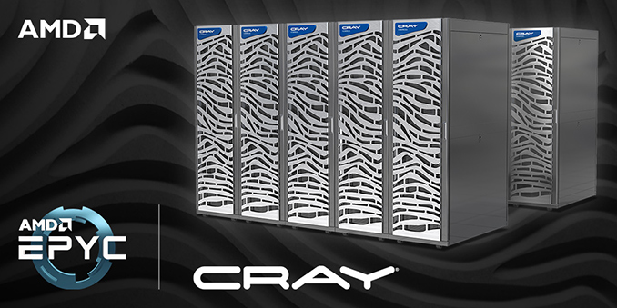
The Cray CS-series supercomputers are built using ultra-dense dual-socket nodes packed into 2U chassis. The CS-series can scale up to 11,000 nodes to provide the right performance and memory capacity for target applications. The AMD-based CS500 systems come with Cray’s software programming environment and libraries that can take advantage of the EPYC processors and their features to maximize performance. An optimized programming environment is a big deal because AMD’s server CPUs have historically suffered from the lack of optimized software.
The Cray CS500 nodes based on AMD EPYC 7000-series processors are dual-socket machines supporting two PCIe 3.0 Gen 3 x16 slots, eight DDR4 memory channels/slots per socket, and a choice of SSD/HDD storage solutions. Four of such machines can fit into a 2U chassis which is then placed into a cabinet. Two aforementioned PCIe slots per machine can be used to plug in two 100 GbE network cards and provide up to 200 Gb/s network connectivity.
For workloads that demand a huge amount of memory, Cray will offer dual-socket 2U CS500 nodes powered by two AMD EPYC 7000 CPUs and featuring 16 DDR4 DIMM slots per socket, thus supporting up to 4 TB of memory per box.
Cray plans to make its AMD EPYC-based CS500 supercomputers available in summer 2018. Prices will depend on actual configurations, which will be disclosed when the systems become available later this year.
Related Reading:
- More EPYC Servers: Dell Launches 1P and 2P PowerEdge for HPC and Virtualization
- Microsoft Announces Azure VMs with Dual 32-core AMD EPYC CPUs
- HPE Unveils ProLiant DL385 Gen10: Dual Socket AMD EPYC
- Dissecting Intel's EPYC Benchmarks: Performance Through the Lens of Competitive Analysis
- AMD Announces Wider EPYC Availability and ROCm 1.7 with TensorFlow Support
- AMD's Future in Servers: New 7000-Series CPUs Launched and EPYC Analysis
More...
-
04-20-18, 08:39 AM #8053
Anandtech: Improving The Exynos 9810 Galaxy S9: Part 2 - Catching Up With The Snapdra
Following our review of the Galaxy S9 there’s been a lot of discussion about both the performance and battery life of Exynos 9810 variants of the Galaxy S9. In the original review I had identified a few key issues with the platform for which I had deemed to be the most negatively attributing to the bad characteristics of the phone. In a first piece following the review I did a few minor changes to the kernel which already seemed to have benefited battery life in our web browsing test, and slightly changing the performance characteristics of the phone for the positive. In this piece we're going further and investigate the performance and battery life impacts.
More...
-
04-20-18, 10:48 AM #8054
Anandtech: Intel Shuts Down New Devices Group: No More Intel-Made Wearables
Intel this week confirmed that it had decided to close down its New Devices Group, which developed various wearable electronics, such as smartwatches, health/fitness monitors, smart/AR glasses and so on. The group was created five years ago by then-incoming CEO Bryan Krzanich, who wanted to ensure that Intel’s chips would be inside millions of emerging devices. While wearables have become relatively popular, their propagation is far below that of smartphones. Meanwhile, wearables made by Intel have never been among the market's bestsellers. Thus, the chip giant is pulling the plug.
Over the five-year history of NDG, Intel made two significant acquisitions to bring necessary expertise to the group: the company took over Basis (a maker of fitness watches) in 2014 and Recon (a maker of wearable heads-up displays) in 2015. Most recently, Intel’s NDG showcased their Vaunt (aka Superlight) smart glasses that looked like “normal” glasses, yet used laser beams to project information to retina justifying their “smart” moniker. While NDG had cutting edge technologies, the group has never managed to produce a truly popular product. Moreover, when problems with one of their Basis smart watches showed up on a limited number of devices, Intel preferred to stop their sales and refund their costs to the customers rather than fix the problems and replace faulty units.
In the second half of 2015, Intel folded the New Devices Group into the New Technology Group, which was a signal that the company was hardly satisfied with NGD’s performance. Since then, we have seen multiple reports about layoffs in Intel’s NGD and have hear multiple rumors to axe the unit. Because making actual devices is generally unnatural for Intel, it was a matter of time brefore the chip giant was to pull the plug, so apparently it decided to do so this month.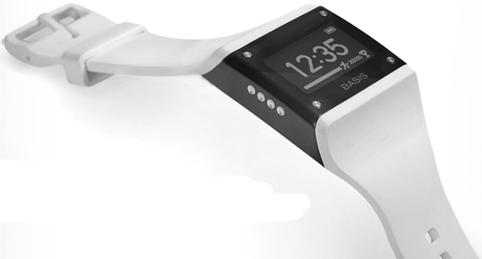
Since Intel’s New Technology Group remains in place, all of Intel’s ongoing research projects for smart devices remain intact. More importantly, other Intel’s divisions continue to work on their products for wearables and ultra-low-power devices that will become widespread in the looming 5G era. The only products that are not going to see the light of day are those designed by Intel’s New Devices Group (e.g., the Vaunt glasses). Considering the fact that neither of NDG’s products has become popular, it is unclear whether those products are going to be missed.
It is noteworthy that Intel canned their Galileo, Joule, and Edison product lines aimed at the Internet-of-Things last Summer.
Related Reading:
- Apple 2017: Announcing a new Apple Watch Series 3, with Intel LTE/Cellular
- IDF 2014: Intel Edison Development Platform Now Shipping
- Intel Announces Galileo: Quark Based Arduino Compatible Developer Board
- Intel Announces “Quark” SoC Family: Tiny SoCs For Tiny Devices
More...
-
04-20-18, 12:58 PM #8055
Anandtech: BenQ Unveils EX3203R 32-inch Curved LCD with FreeSync 2, DCI-P3, & USB-C
AMD’s FreeSync 2 platform this week gained yet another supporter. BenQ on Thursday introduced its EX3203R gaming display that supports AMD’s latest dynamic refresh rate technology along with the DCI-P3 color gamut. BenQ’s new monitor will be the fifth FreeSync 2-supporting LCD announced so far and thus will have only a few competitors. It is also noteworthy that the EX3203R will have a USB Type-C input, a feature not available on other displays with FreeSync 2.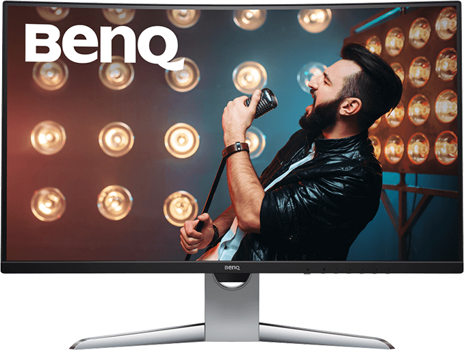
BenQ’s EX3203R is based on a 32-inch curved VA panel featuring a 2560×1440 resolution, 400 nits brightness, a 3000:1 contrast ratio, 178°/178° viewing angles, a 4 ms response time, and a 144 Hz maximum refresh rate. The key feature of the monitor is AMD’s FreeSync 2 dynamic refresh rate technology that mandates support of at least 90% of the DCI-P3 color space along with HDR and LFC (low framerate compensation). BenQ does not specify the range of the FreeSync 2 on the EX3203R monitor, but from our previous encounters with 32-inch FreeSync 2-supporting displays, it is reasonable to expect the new model to feature a relatively wide range from at least 72 Hz to 144 Hz.
Speaking of FreeSync 2-supporting displays in general, it is noteworthy that all 32-inch FreeSync 2 LCDs announced to date use a VA panel with a 2560×1440 resolution, a 400 nits brightness, and a 1800R curvature. While no official comments have been made on this matter, it is highly likely that AOC’s AGON AG322QC4, BenQ’s EX3203R, and Samsung’s C32HG70 are based on the same 32-inch VA panel from the Korean company. Meanwhile, Samsung itself uses a QLED backlighting (with quantum dots) to guarantee coverage of up to 95% of the DCI-P3 color space, whereas other suppliers use P3-graded LED backlighting that enables coverage of “only” 90% of this color gamut.
Back to the BenQ EX3203R. The display comes in a plastic chassis and has a stand that can adjust height, and tilt. As for connectivity, the monitor is outfitted with two HDMI 1.4 inputs, one DisplayPort 1.2 header, a USB Type-C port that can be used to connect laptops, and a mini-jack for headphones. The EX3203R is also equipped with a dual-port USB 3.0 Type-A hub that uses the USB Type-C as an upstream port.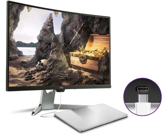
Gallery: BenQ Unveils EX3203R 32-inch Curved LCD with 144 Hz, FreeSync 2, DCI-P3 & USB-CThe BenQ EX3203R General Specifications Panel 31.5" VA Native Resolution 2560 × 1440 Maximum Refresh Rate 144 Hz Response Time 4 ms GtG Brightness 400 cd/m² (peak) Contrast 3000:1 Backlighting LED Viewing Angles 178°/178° horizontal/vertical Curvature 1800R Aspect Ratio 16:9 Color Gamut >95% sRGB/BT.709
90% DCI-P3DisplayHDR Tier 400 (unconfirmed) Dynamic Refresh Rate Tech AMD FreeSync 2 Pixel Pitch 0.2767 mm² Pixel Density 91.79 PPI Inputs 1 × DisplayPort 1.2
2 × HDMI 1.4
1 × USB Type-C
HDCP 2.2 supportedAudio 3.5 mm output USB Hub 2 × USB 3.0 Type-A connectors
1 × USB 3.0 Type-C inputAdjustments Height: ±60 mm
Tilt: -5? - 20?MSRP unknown 


In addition to its key selling points like FreeSync 2 support, a very high refresh rate, a USB-C input, and a curvature, the BenQ EX3203R also has very thin bezels and supports various enhancements from the manufacturer, such as the Brightness Intelligence Plus and the Low Blue Light. The BI+ detects surrounding light levels and automatically adjusts brightness and color temperature to fit the environment (professionals would hate this feature). In addition, the same tech can adjust brightness based on usage time to protect user’s eyes (this one will hardly be appreciated by both professionals and gamers). As for the LBL, it can filter blue light to reduce eye fatigue.
BenQ has not announced ETA or MSRP for the EX3203R, but it makes sense to expect the display on store shelves in the coming weeks or months.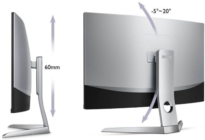
Related Reading:
- AOC Announces AGON AG322QC4 32-Inch Curved LCD with FreeSync 2 & DisplayHDR 400
- Samsung Announces First Freesync 2 Monitors: CHG70 & CHG90 - Quantum Dots, Up to 49”, 144 Hz, DCI-P3
- AMD Announces FreeSync 2: Easier & Lower Latency HDR Gaming
- Microsoft and AMD to Bring FreeSync 2 Support to Xbox One S and Xbox One X This Spring
More...
-
04-23-18, 02:32 PM #8056
Anandtech: AMD Launches Ryzen 3 2200GE & Ryzen 5 2400GE 35 W APUs
AMD has officially added energy-efficient Ryzen 3 and Ryzen 5 APUs to its product lineup. The new processors with integrated Radeon Vega graphics, have a 35 W TDP, and at this point in time will only be initially available to system integrators enabling the latter to build small form-factor PCs, rather than directly selling at retail.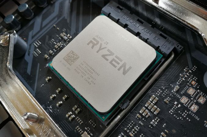
AMD’s Ryzen 3 2200GE and Ryzen 5 2400GE APUs pack four Zen cores running at 3.2 GHz default frequency (with multithreading for the Ryzen 5) and integrated Radeon Vega 8 or Radeon Vega 11 graphics respectively. In a bid to reduce TDP of the APUs to 35 W compared to the 65W vresions, AMD had to reduce clocks of the GE chips by 300-400 MHz as showin in the table below. For the integrated graphics, they remain untouched: the Ryzen 3 2200GE has 512 stream processors at 1100 MHz, whereas the Ryzen 5 2400GE has 704 SPs at 1250 MHz. The supported memory controller also retains parity: two DDR4 memory channels up to DDR4-2933.
The new APUs from AMD featuring a 35 W TDP are designed for the AM4 socket, but need appropriate BIOS support by the motherboards. As the Ryzen 3 2200GE and the Ryzen 5 2400GE are made available to system integrators first, their drop in compatibility with retail motherboards is not a priority for AMD just now. Motherboard makers, namely ASUS, have been adding support for the new APUs to their BIOSes in the last few weeks.
Despite the fact that AMD lists the new 35W APUs on its website, the company has not included the chips into its pricelist and it is unknown how much do they cost. Retail versions of AMD’s 65W Ryzen 5 2400G and Ryzen 3 2200G are priced at $169 and $99 respectively and come with coolers - it is likely that the tray prices of the 35W parts will be slightly beneath this.AMD Ryzen 2000-Series APUs Ryzen 5
2400G
Vega 11Ryzen 5
2400GE
Vega 11Ryzen 3
2200G
Vega 8Ryzen 3
2200GE
Vega 8Cores 4 / 8 4 / 4 Base CPU Freq 3.6 GHz 3.2 GHz 3.5 GHz 3.2 GHz Turbo CPU Freq 3.9 GHz 3.8 GHz 3.7 GHz 3.6 GHz TDP @ Base 65 W 35 W 65 W 35 W cTDP 46-65 W 35 W 46-65 W 35 W L2 Cache 512 KB/core L3 Cache 4 MB Graphics Vega 11 Vega 8 Compute Units 11 CUs 8 CUs Streaming Processors 704 SPs 512 SPs Turbo GPU Freq 1250 MHz 1100 MHz DRAM Support DDR4-2933 Dual Channel OPN PIB YD2400C4FBBOX ? YD2200C5FBBOX ? OPN Tray YD2400C5M4MFB YD2400C6M4MFB YD2200C4M4MFB YD2200C6M4MFB Price $169 ? $99 ? Bundled Cooler Wraith Stealth None w/Tray Wraith Stealth None w/Tray
Related Reading- AMD Readies Ryzen 3 2200GE & Ryzen 5 2400GE APUs with Reduced TDP
- Marrying Vega and Zen: The AMD Ryzen 5 2400G Review
- AMD Tech Day at CES: 2018 Roadmap Revealed, with Ryzen APUs, Zen+ on 12nm, Vega on 7nm
More...
-
04-23-18, 04:14 PM #8057
Anandtech: Intel Lists New Atom Core: Tremont to Come After Goldmont Plus
Intel has recently updated its developer documentation for instruction set extensions, and in the process has disclosed information on both new instructions for and the codename of its next-generation low-power processor microarchitecture. Dubbed "Tremont", the forthcoming processor core look to replace Goldmont Plus in the upcoming Atom, Celeron, and Pentium Silver-branded SoCs.
According to the Intel Architecture Instruction Set Extensions (ISE) and Future Features Programming Reference document, the Goldmont Plus microarchitecture will not be the end of the road for Intel’s low-cost/low-power cores. In the coming years it will be succeeded by the codenamed Tremont microarchitecture and its successors. On the manufacturing side of matters, nothing has officially been disclosed, but right now our suspicion is that processors based on the Tremont will be made using the company’s 10 nm process technology. To date we haven't seen Intel use their enhanced “+” and “++” 14nm process technologies to make SoCs for entry-level and energy-efficient PCs - as the original 14nm provides better density - so it seems unlikely that Intel would start now.
A key question about the Tremont is what architecturaly improvements it will bring. While Intel's document does specify the new instructions, it doesn't offer any general architectural insight. Intel's general trend thus far since Silvermont has been to gradually widen their out-of-order execution design, starting with two-way, moving to three-way (Goldmont), and then to a three-way front-end plus a four-way allocation and retirement backend. So it may be that we see Intel go this route, as they already have a number of tricks left in their bag from Core, and it meshes well with the high density aspects of their 10nm processes, which favors more complex processors.
As for the ISE improvements, Intel’s Tremont will feature CLWB, GFNI (SSE-based), ENCLV, and Split Lock Detection instruction set extensions, which are also set to arrive with Intel’s Ice Lake processors. Also set to arrive with Tremont will be CLDEMOTE, direct store, and user wait instructions (see details in the table below). Unlike the earlier instructions, these are unique to Tremont and are not scheduled to be supported by the Ice Lake (or other documented Intel’s cores).
The fact that Intel is readying its “Future Tremont and later” microarchitectures reveals that even after the company withdrew from smartphone SoCs, it sees plenty of applications that could use its low-power/low-cost Atom cores. There is sitll a notable market for budget PCs as well as embedded and semi-embeded markets for items like IoT edge devices, all of which Intel intends to continue serving with the line of smaller, cheaper cores. Meanwhile, consistent ILP and performance improvements as well as introduction of new ISEs to these microarchitectures show that Intel wants these cores to offer competitive performance to other low-cost processors, while still maintaining near feature set parity to Intel's high-performance cores.New Instruction Set Extensions of Goldmont Plus and Tremont CPUs Instruction Purpose Description Goldmont Plus PTWRITE
Write Data to a Processor Trace PacketDebugging Unclear. UMIP
User-Mode Instruction PreventionSecurity Prevents execution of certain instructions if the Current Privilege Level (CPL) is greater than 0. If these instructions were executed while in CPL > 0, user space applications could have access to system-wide settings such as the global and local descriptor tables, the task register and the interrupt descriptor table. RDPID
Read Processor IDGeneral Quickly reads processor ID to discover its feature set and apply optimizations/use specific code path if possible. Tremont CLWB
Cache Line
Write BackPerformance Writes back modified data of a cache line similar to CLFLUSHOPT, but avoids invalidating the line from the cache (and instead transitions the line to non-modified state). CLWB attempts to minimize the compulsory cache miss if the same data is accessed temporally after the line is flushed if the same data is accessed temporally after the line is flushed. GFNI (SSE) Security SSE-based acceleration of Galois Field Affine Transformation alghorithms. ENCLV Security Further enhancement of SGX version 1 capabilities. CLDEMOTE Performance Enables CPU to demote a cache line with a specific adress from the nearest cache to a more distant cache without writing back to memory. Speeds up access to this line by other cores within a CPU. Direct stores: MOVDIRI, MOVDIR64B Performance User wait: TPAUSE, UMONITOR, UMWAIT Power Direct CPU to enter certain stages before an event happens. Split Lock Detection Source: Intel Architecture Instruction Set Extensions and Future Features Programming Reference (pages 12 and 13)
Related Reading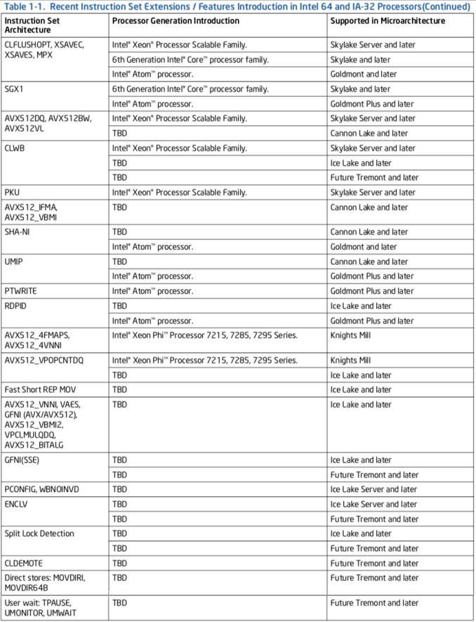
- Intel Launches New Pentium Silver and Celeron Atom Processors: Gemini Lake is Here
- Intel Documents Point to AVX-512 Support for Cannon Lake Consumer CPUs
- Intel Quietly Launches Apollo Lake SoC: Goldmont CPU, 6 SKUs, 6 & 10 Watts
- Intel's Changing Future: Smartphone SoCs Broxton & SoFIA Officially Cancelled
Sources: Intel, WikiChip
More...
-
04-24-18, 11:10 AM #8058
Anandtech: The Mainstream Phoenix Rises: Samsung's 970 EVO (500GB & 1TB) SSDs Reviewe
The new Samsung 970 EVO isn't their top of the line consumer SSD, but it might as well be. With their latest 3D TLC NAND flash memory and SSD controller, the 970 EVO offers almost all the performance of its PRO counterparts but without such a steep price premium.
More...
-
04-24-18, 11:10 AM #8059
Anandtech: Samsung Announces 970 PRO And 970 EVO NVMe SSDs
Samsung has announced the third generation of their high-end consumer NVMe SSDs. The new 970 PRO and 970 EVO M.2 NVMe SSDs use a newer controller and Samsung's latest 64-layer 3D NAND flash memory. The outgoing 960 PRO and 960 EVO were first announced in September 2016 and shipped that fall, so they have had a fairly long run as Samsung's flagship consumer SSDs.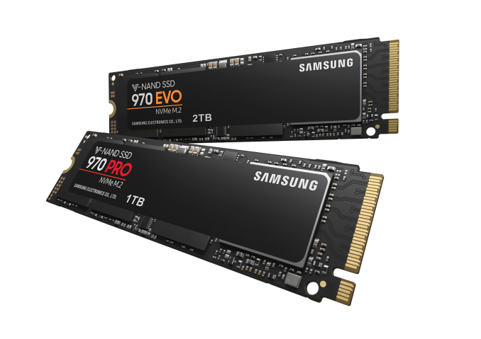
There are no big surprises from today's announcement. Samsung's transition to 64-layer 3D NAND has been underway for a year, and the retail SATA lineup migrated to the fourth-generation 3D NAND earlier this year. This generation of NAND includes a 512Gb TLC die that allows for 1TB in a single BGA package, so squeezing 2TB onto a single-sided M.2 2280 card is no longer a challenge.
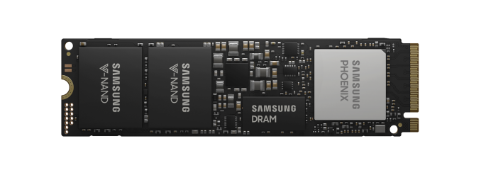
The Samsung Phoenix controller used in the 970s has been on our radar for a long time after appearing on many of Samsung's recent NVMe SSDs for other markets: the PM981 client SSD for OEMs, the PM983 enterprise SSD that is being used to promote Samsung's new NF1 (formerly NGSFF) form factor, and the high-end enterprise Z-SSD SZ985.
Buy Samsung PM981 on Amazon.com
Samsung's retail NVMe SSD product numbering is now out of sync with their OEM and enterprise SSDs. This is because the Samsung PM971 wasn't a direct replacement for anything in the 96x generation. Instead, the PM971 is a low-end BGA SSD featuring Samsung's Photon controller instead of the 96x generation's Polaris or the current Phoenix. BGA SSDs are obviously not a good fit for the retail SSD market, and even when mounted on M.2 cards the PM971 would have had a fairly small audience. Samsung's retail NVMe SSDs aren't skipping over the 970 generation, but their other high-end NVMe drives did.
Samsung is still using MLC NAND for the PRO series and TLC NAND for the EVO series. However, it is clear that the TLC-based EVO is the more important product for Samsung. The PRO series has been reduced back down to just two capacities (512GB and 1TB), while the EVO now spans from 250GB up to 2TB. The EVO series now also matches the PRO's 5-year warranty term. Other manufacturers have started to abandon MLC NAND completely for their consumer product lines. Samsung isn't quite there yet, but the PRO is looking like even more of a niche product this time around. We have not seen a MLC-based SM981 drive, so it seems likely that the client OEM product line is done using MLC NAND.
We were impressed with the PM981 drives we had the opportunity to test in November. We found that the combination of updated NAND and the new Phoenix controller provided a solid generational boost over the 960 EVO, often bringing performance up to the level of the 960 PRO and occasionally surpassing it. The retail 970s are a bit overdue, because several recent competing NVMe SSDs had made it clear that the 960s were losing the lead. The 970 EVO on its own probably won't be enough for Samsung to reestablish an undisputed lead in M.2 SSD performance.Samsung 970 EVO Specifications Capacity 250 GB 500 GB 1 TB 2 TB Interface PCIe 3 x4 NVMe 1.3 Form Factor M.2 2280 Single-sided Controller Samsung Phoenix NAND Samsung 64-layer 256Gb 3D TLC Samsung 64L 512Gb 3D TLC LPDDR4 DRAM 512 MB 1 GB 2 GB SLC Write Cache Dedicated 4 GB 4 GB 6GB 6 GB Dynamic 9 GB 18 GB 36 GB 72 GB Sequential Read 3400 MB/s 3500 MB/s Sequential Write (SLC Cache) 1500 MB/s 2300 MB/s 2500 MB/s 2500 MB/s Sequential Write (TLC) 300 MB/s 600 MB/s 1200 MB/s 1250 MB/s 4KB Random Read QD1 15k IOPS QD128 200k IOPS 370k IOPS 500k IOPS 500k IOPS 4KB Random Write QD1 50k IOPS QD128 350k IOPS 450k IOPS 450k IOPS 480k IOPS Active Power Read 5.4 W 5.7 W 6 W 6 W Write 4.2 W 5.8 W 6 W 6 W Idle Power APST On 30 mW PCIe L1.2 5 mW Write Endurance 150 TB 300 TB 600 TB 1200 TB Warranty 5 years MSRP $119.99 (48¢/GB) $229.99 (46¢/GB) $449.99 (45¢/GB) $849.99 (42¢/GB)
Compared to its predecessor, the 970 EVO promises a small improvement in sequential read speed, and a more substantial boost to sequential write speed for all but the smallest 250GB model. Peak random access performance is also substantially improved, but again the 250GB model gets left out, and is actually rated as slower than the 960 EVO 250GB.
The warranty on the EVO has been extended from three years to five years, and the write endurance ratings have been increased by 50% to retain almost the same drive writes per day rating.
The 970 EVO will debut with prices slightly lower than the launch MSRPs for the 960 EVO. In between the two product launches, a severe industry-wide shortage of flash memory kept prices high, but now that most NAND flash manufacturers have their 64L 3D NAND production in full swing, retail prices are improving.
Samsung has dropped the 2TB option from the PRO lineup, replacing it with a 2TB 970 EVO that is about a third cheaper and will likely be much more popular. That 2TB 970 EVO is the only model using Samsung's 512Gb 64L 3D TLC die, while the smaller models use the 256Gb version.
 The 970 PRO's performance specs aren't too different from the 970 EVO. Many of the ratings are the same, and the ones that differ are mostly better by just 3-11% for the PRO. There are just two major exceptions to this. First, the PRO doesn't rely on SLC write caching so it can maintain its write speed far longer than the EVO. Second, the rated write endurance of the 970 PRO is twice that of the EVO, going from just over 0.3 Drive Writes Per Day to 0.6 DWPD. Neither of these are an important factor for ordinary consumer use cases, but they help the 970 PRO retain some shine as a premium product.
Samsung 970 PRO Specifications Capacity 512 GB 1 TB Interface PCIe 3 x4 NVMe 1.3 Form Factor M.2 2280 Single-sided Controller Samsung Phoenix NAND Samsung 64-layer 3D MLC V-NAND LPDDR4 DRAM 512 MB 1 GB Sequential Read 3500 MB/s Sequential Write 2300 MB/s 2700 MB/s 4KB Random Read QD1 15k IOPS QD128 370k IOPS 500k IOPS 4KB Random Write QD1 55k IOPS QD128 500k IOPS Active Power Read 5.2 W Write 5.2 W 5.7 W Idle Power APST On 30 mW PCIe L1.2 5 mW Write Endurance 600 TB 1200 TB Warranty 5 years MSRP $329.99 (64¢/GB) $629.99 (62¢/GB)
The 970 PRO's improvements over the 960 PRO are mostly for random I/O performance, where both drives are now rated to hit 500k IOPS for random writes, given sufficient queue depth. As with the EVO, rated write endurance has been increased by 50%, but the PRO's warranty remains at 5 years. The MSRPs for the 970 PRO are the same as the the launch prices for the 960 PRO.
Related Reading- The Mainstream Phoenix Rises: Samsung's 970 EVO (500GB & 1TB) SSDs Reviewed
- The Samsung PM981 SSD Review (512GB, 1TB): Next Generation Controller And 3D NAND
- The Western Digital WD Black 3D NAND SSD Review: EVO Meets Its Match
- The Intel Optane SSD 800p (58GB & 118GB) Review: Almost The Right Size
- The Intel SSD 760p 512GB Review: Mainstream NVMe Done Right
- The Samsung 860 PRO (512GB And 4TB) SSD Review: Replacing A Legend
More...
-
04-24-18, 04:19 PM #8060
Anandtech: TSMC Kicks Off Volume Production of 7nm Chips
TSMC last week announced that it had started high volume production (HVM) of chips using their first-gen 7 nm (CLN7FF) process technology. The contract maker of semiconductors says it has over a dozen of customers with tens of designs eager to use the technology to make their integrated circuits.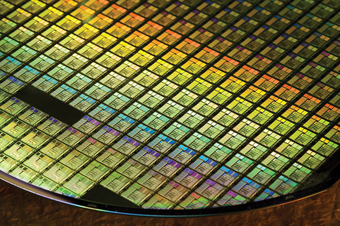
The 7 nm node is a big deal for the foundry industry in general and TSMC in particular. When compared to the CLN16FF+ technology (TSMC’s most widely used FinFET process technology) the CLN7FF will enable chip designers to shrink their die sizes by 70% (at the same transistor count), drop power consumption by 60%, or increase frequency by 30% (at the same complexity). So far, TSMC has taped out 18 customer products using the CLN7FF technology, more than 50 CLN7FF products will be taped out by the end of 2018.
Unlike TSMC’s CLN10FF, which is used by a limited number of customers for a limited number of mobile SoCs, the CLN7FF is expected to be used to build CPUs, GPUs, FPGAs, neural network processors, cryptocurrency mining accelerators, mobile SoCs and so on. This is important because demand for smartphones is slowing down and TSMC needs other customers to offset lower orders for mobile SoCs.
“So far, we have already favored out more than 18 customer products with good yield [and] performance,” said C. C. Wei, a Co-CEO and President of TSMC, during a conference call with financial analysts. “More than 50 products tape-outs has been planned by end of this year from applications across mobile, server CPU, network processor, gaming, GPU, PGA, cryptocurrency, automotive and AI. Our 7nm is already in volume production.”
TSMC’s CLN7FF process technology will rely on deep ultraviolet (DUV) lithography with argon fluoride (ArF) excimer lasers operating on a 193 nm wavelength. As a result, the world’s largest contract maker of semiconductors will be able to use existing manufacturing tools to make 7 nm chips. Meanwhile, to keep using DUV lithography the company and its customers have to use multipatterning (triple and quadruple patterning), which increases design and production costs as well as product cycles.
Next year TSMC intends to introduce its first manufacturing tech that will use extreme ultraviolet lithography (EUVL) for select layers. The CLN7FF+ will be the company’s second-generation 7 nm fabrication process because of design rules compatibility and because it will keep using DUV tools that TSMC uses today for its CLN7FF production. From a general PPA (power, performance, area) improvement point of view, TSMC expects its CLN7FF+ to offer a 20% higher transistor density and a 10% lower power consumption at the same complexity and frequency when compared to the CLN7FF. Furthermore, TSMC’s EUV-based 7 nm technology could also feature higher performance and a tighter distribution of currents, but the company’s execs do not quantitate the improvements just now.Advertised PPA Improvements of New Process Technologies
Data announced by companies during conference calls, press briefings and in press releasesTSMC 16FF+
vs
20SOC10FF
vs
16FF+7FF
vs
16FF+7FF
vs
10FF7FF+
vs
7FFPower 60% 40% 60% 50% 70% >37% ~17%
“Our N7+ silicon result today are very encouraging,” said Mr. Wei. “Not only we have demonstrated equivalent or better performance [and] yield on both 256 Mb SRAM and on product like test vehicle when compared to [the] N7 baseline, we have also demonstrated a tighter distribution of electrical parameters in the areas, where EUV is supplied.”
TSMC is on track to start HVM using its 7 nm EUV process technology in mid-2019. Going forward, the company will increase usage of ASML’s Twinscan NXE step and scan systems when it starts to process wafers using its CLN5 (5 nm) process technology in 2020. According to the co-CEO of TSMC, the EUV results have been encouraging so far: the company’s 256 Mb SRAM test chip is already made with a “consistent double-digit yield”, which is rather good for a technology that is two years away from HVM. The high-ranking executive of TSMC also noted that the EUV infrastructure in general has made a good progress in the recent quarters. In particular, the company observed lower pellicle defects, higher mask yields, and improved photoresists.
Related Reading:
- Samsung and TSMC Roadmaps: 8 and 6 nm Added, Looking at 22ULP and 12FFC
- TSMC Teams Up with ARM and Cadence to Build 7nm Data Center Test Chips in Q1 2018
- GlobalFoundries Details 7 nm Plans: Three Generations, 700 mm², HVM in 2018
- The Future of Silicon: An Exclusive Interview with Dr. Gary Patton, CTO of GlobalFoundries
More...


 Quote
QuoteThread Information
Users Browsing this Thread
There are currently 18 users browsing this thread. (0 members and 18 guests)


Bookmarks