

Results 8,601 to 8,610 of 12096
Thread: Anandtech News
-
09-06-18, 08:36 AM #8601
Anandtech: AMD Announces New $55 Low-Power Processor: Athlon 200GE
Everyone lines discussing headlines: the latest mainstream processor, or super 32-core behemoth, are topics ripe for deep discussion. Despite this, a lot more volume occurs in the mid-range and low-end of the product stack. Never mind $299 for a CPU, there is a lot of action that occurs under $100. With that in mind, AMD is announcing its new $55 processor with integrated graphics, designed to sit under the Ryzen 5 2200G that we tested earlier this year. The Athlon 200GE by comparison has two cores with simultaneous multi-threading, three compute units for graphics, and a 35W TDP, all for $55.
More...
-
09-06-18, 09:32 AM #8602
Anandtech: Corsair Launches Elgato Thunderbolt 3 Mini Dock
Corsair on Thursday introduced its first Elgato-branded miniature Thunderbolt 3 dock. The product has two 4Kp60-capable display outputs, a USB Type-A port, and a Gigabit Ethernet connector.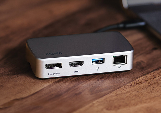
The minimalistic Elgato Thunderbolt 3 Mini Dock is aimed primarily at owners of Apple’s latest MacBook Pro laptops who need an essential set of ports while on the go. The Thunderbolt 3 Mini Dock has one DisplayPort 1.2 output, an HDMI 2.0 output (with HDCP support), a USB 3.1 Gen 1 Type-A port (5 Gbps, up to 1.1 A), and a GbE port.
Being very compact, the Thunderbolt 3 Mini Dock weighs 125 grams (4.4 ounces), looks like a big pack of mints, and comes with a foldable 12 cm (4.7 inch) cable that can be quickly hidden when not in use as well as easily managed when in use.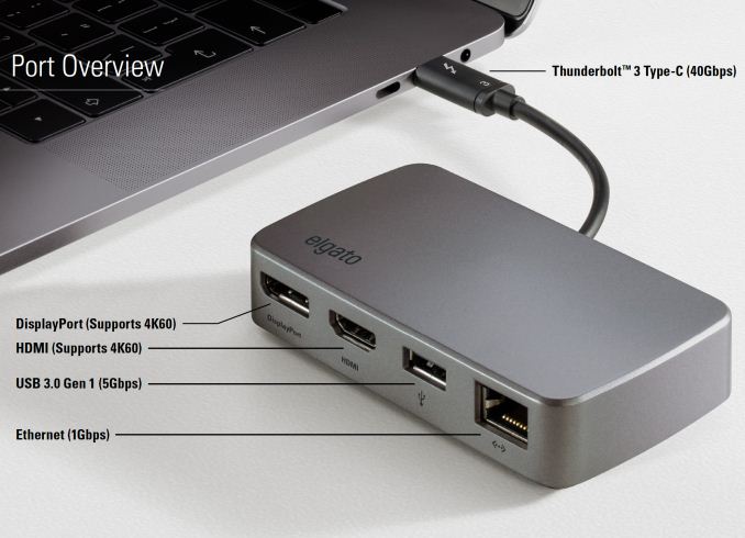
When it comes to compatibility, the Elgato Thunderbolt 3 Mini Dock will work with Apple’s macOS High Sierra 10.13 or later as well as with Microsoft’s Windows 10 and later. Unfortunately Corsair does not disclose which Thunderbolt 3 controller it uses for its TB3 Mini Dock – whether they're using Alpine Ridge or the new USB 3-compatible Titan Ridge – however the exclusion of any mention of USB 3 compatibility in the official specifications strongly points to the tradtional Alpine Ridge, making this a true TB3-only dock.
Meanwhile, to make the Elgato Thundebolt 3 Mini Dock more attractive to owners of various Apple devices, the product comes with the Elgato Dock Utility for macOS that enables high-power USB support and easy ejection of storage devices attached to the dock.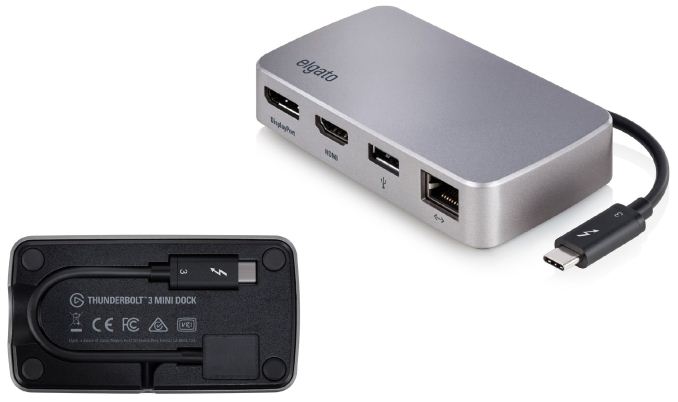
Corsair’s Elgato Thunderbolt 3 Mini Dock will hit the market shortly. In the U.S. it will cost $149, while in other countries prices will be different.
Related Reading: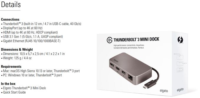
- Corsair Takes Over Gaming, Video Capture, & Docking Assets from Elgato
- StarTech Launches ‘Affordable’ Thunderbolt 3 ‘Mini Docks’: USB-A, GbE, DP or HDMI
- StarTech’s New Adapter Brings eSATA Storage to Thunderbolt 3 PCs
- StarTech Launches Thunderbolt 3 USB Hub with 3 USB 3.1 Controllers & Power Delivery
- StarTech's Thunderbolt 3 to Dual 4Kp60 Display Adapters Now Available
- Promise Launches TD-300 9-in-1 Thunderbolt 3 Dock: GbE, HDMI, USB 3.0, TB3 Charging & More
- OWC Launches 13-Port Thunderbolt 3 Dock: GbE, USB-A, SD Card, mDP, FireWire & More
- StarTech Unveils Dual-Display Thunderbolt 2 Docking Station with 12 Ports
- AKiTiO Displays Thunderbolt 3 to 10GBase-T Adapter
More...
-
09-06-18, 10:08 AM #8603
Anandtech: Samsung Foundry Updates: 8LPU Added, EUVL on Track for HVM in 2019
Samsung recently hosted its Samsung Foundry Forum 2018 in Japan, where it made several significant foundry announcements. Besides reiterating plans to start high-volume manufacturing (HVM) using extreme ultraviolet lithography (EUVL) tools in the coming quarters, along with reaffirming plans to use gate all around FETs (GAAFETs) with its 3 nm node, the company also added its brand-new 8LPU process technology to its roadmap.
10 nm Node Lives On
Samsung Foundry’s general roadmap was announced earlier this year, so at SFF in Japan the contract maker of semiconductors reiterated some of its plans, made certain corrections, and provided some additional details about its future plans.
First up, Samsung added another fabrication technology into its family of manufacturing processes based on its 10 nm node. The new tech is called 8LPU (low power ultimate) and, according to Samsung’s usual classification, this is a process for SoCs that require both high clocks and high transistor density. Samsung’s 8LPP technology, which qualified for production last year, is a development of Samsung’s 10 nm node that uses narrower metal pitches to deliver a 10% area reduction (at the same complexity) as well as a 10% lower power consumption (at the same frequency and complexity) compared to 10LPP process. 8LPU is a further evolution of the technology platform that likely increases transistor density and frequency potential vs 8LPP. Meanwhile Samsung does not disclose how it managed to improve 8LPU vs. 8LPP and whether it involved advances of design rules, usage of a new library, or a shrink of metal pitches.
Samsung’s 8LPP and 8LPU technologies are aimed at customers who need higher performance or lower power and/or higher transistor density than what Samsung’s 10LPP, 10LPC, and 10LPU processes can offer, but who cannot gain access to Samsung’s 7LPP or more advanced manufacturing technologies that use EUVL. Risk production using 8LPU was set to start in 2018, so expect high-volume manufacturing to commence next year at Samsung’s Fab S1 in Giheung, South Korea.
7LPP EUV on Track
Last year Samsung Foundry promised to start risk production of chips using its 7LPP fabrication technology in 2018. As it appears, it has initiated manufacturing of certain 7LPP SoCs, though presumably only for its parent company, as its MPW shuttle service schedule does not mention 7LPP at all. The production tech will be Samsung Foundry’s flagship process, so expect the company to use it first for its parent company’s mobile SoCs. Meanwhile, the process tech is also suitable for larger chips aimed at HPC, ML, and AI markets (think CPUs, specialized SoCs, etc.). For example, Samsung is prepping specialized IP for appropriate chips, including 100 Gbps+ SerDes and other.
At the forum, Samsung Foundry said that it had installed multiple ASML Twinscan NXE:3400B EUVL step and scan systems at its Fab S3 in Hwaseong, South Korea. The company naturally does not disclose how many of such tools have been installed, but it indicated that wafer per day (WPD) performance of the said scanners is in line with its mass production targets. As reported before, the first manufacturing processes that will take advantage of EUVL will use it for select layers only, so do not expect extensive usage of the new equipment initially. In fact, since EUV will be used for HVM for the first time in the industry, Samsung Foundry is hardly inclined to expand its usage beyond select customers and designs (think Samsung Electronics and Qualcomm, which has already selected 7LPP for its Snapdragon 5G SoC due in 2019).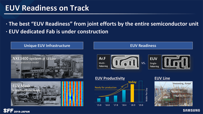
A radical expansion of EUV lithography usage by Samsung Foundry will occur after it builds another production line in Hwaseong, which will be architected for the EUV equipment from the start. The line is set to cost 6 trillion Korean Won ($4.615 billion), it is expected to be completed in 2019, and start HVM in 2020. As a result, Samsung’s production involving EUVL equipment will be limited to one fab for at least several quarters down the road. Generally, this is a reason why Samsung Foundry has developed its 8LPP and 8LPU process technologies.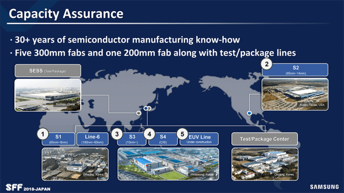
5/4 nm to Hit Risk Production in 2019
By the time the new production line in Hwaseong becomes operational, Samsung Foundry promises to start risk production using its 5/4 nm node. As reported earlier this year, Samsung is prepping 5LPE, 4LPE, and 4LPP fabrication technologies, but eventually this list will likely expand. Based on what Samsung has disclosed about all three manufacturing processes so far, they will have certain similarities, which will simplify migration from 5LPE all the way to 4LPP, though the company does not elaborate.
One of the slides the company demonstrated at SFF 2018 Japan indicates that Samsung expects risk production of chips using the 5/4 nm node to commence in 2019, indicating that the process technologies will coexist rather than follow each other. Since there are hardly any reason for Samsung to design competing fabrication processes, it is more likely that its 5LPE will be used for HVM first in 2020 and then 4LPE/4LPP will follow later on expanding usage of EUV equipment, unless Samsung’s roadmap changes significantly and certain offerings get canned (which tends to happen).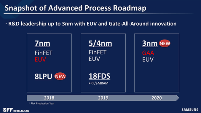
One of the things to keep in mind is that Samsung’s 5/4 nm will be the company’s last node to use FinFET transistors, which is why it will be “long” node that will be used for many years to come, just like the 28 nm technology is used today and will stay here for a long time.
3 nm Pulled In?
One of the unexpected things that Samsung Foundry announced was start of risk production using its 3 nm node already in 2020, which is at least a year ahead of what was expected earlier. Samsung’s 3 nm will be the first node to use the company’s own GAAFET implementation called MBCFET (multi-bridge-channel FETs) and will officially include at least two process technologies: 3GAAE and 3GAAP (3nm gate-all-around early/plus).
Samsung still did not announce any HVM targets for 3GAAE and 3GAAP and it is hard to say when exactly the company adopts its MBCFET-based technologies for commercial SoCs. What we do understand today is that both technologies will rely on EUVL, so before using either Samsung will have to make sure that EUV delivers the necessary yields and production performance. Considering the fact that Samsung is satisfied with performance of its ASML Twinscan NXE:3400B EUVL step and scan systems today and expects further increases of WPD productivity, it is possible that it pulled in its 3 nm node.
18FDS Risk Production Due in 2019
Although GAAFETs are only several years away, technologies based on planar transistors are not going anywhere and keep evolving. Samsung Foundry will continue to back FD-SOI technology going forward and will offer a formidable rival for GlobalFoundries’ 22FDX and 12FDX offerings.
Samsung Foundry intends to start risk production of chips using its 18FDS already in 2019, so expect HVM in 2020 at the latest. The tech uses the same BEOL interconnects as Samsung’s 14LPE/14LPP technologies (i.e., BEOL originally developed for its 20 nm planar process), but with new transistors and FEOL. The company promises that when compared to its 28FDS, its 18FDS will enable a 20% higher performance (at the same complexity and power), a 40% lower power (at the same frequency and complexity), and a 30% lower die area.
What is particularly important is that 18FDS will support both RF and eMRAM, allowing Samsung Foundry to target a wide variety of applications that require RF and embedded memory in the 5G era in 2020 and onwards.
3D System-in-Package Ready in 2019
Chip packaging technologies are gaining importance these days as it becomes increasingly hard and expensive to integrate everything into a single processor. Samsung (just like TSMC and GlobalFoundries) already has a number of package solutions for complex products, such as FOPLP-PoP for mobile SoCs and I-Cube (2.5D) for chips that use HBM2 DRAMs. Next year the company will offer its 3D SiP (system-in-package) solution that will enable it to pack a variety of devices into a single three-dimensional package with a small footprint.
Samsung Foundry’s 3D SiP will be one of the industry’s first technology of its kind that will be used to build heterogeneous 3D SiPs (currently all SiPs are 2D). The package solution will enable the contract maker of semiconductors to assemble SiPs using components made using entirely different process technologies.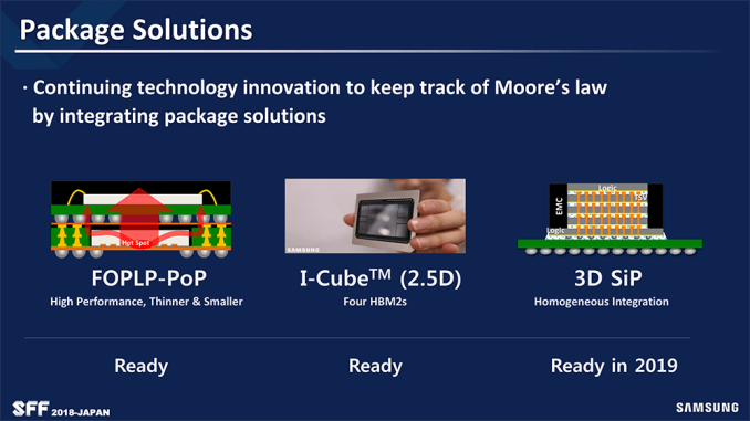
Related Reading:
- Samsung Foundry Roadmap: EUV-Based 7LPP for 2018, 3 nm Incoming
- Arm and Samsung Extend Artisan POP IP Collaboration to 7LPP and 5LPE Nodes
- Samsung’s 8LPP Process Technology Qualified, Ready for Production
- Samsung and TSMC Roadmaps: 8 and 6 nm Added, Looking at 22ULP and 12FFC
- TSMC Details 5 nm Process Tech: Aggressive Scaling, But Thin Power and Performance Gains
- Intel Delays Mass Production of 10 nm CPUs to 2019
- TSMC Kicks Off Volume Production of 7nm Chips
- TSMC Starts to Build Fab 18: 5 nm, Volume Production in Early 2020
Source: PC Watch
More...
-
09-06-18, 12:00 PM #8604
Anandtech: UL Delists Huawei Devices Due To Inaccurate Benchmarks
A few days ago we published our article addressing Huawei and Honor’s inaccurate benchmarking behaviour. In a nutshell, we had found out that this year’s devices had introduced a new thermal limiting behaviour that quickly throttled power consumption to ~4-4.5W in 3D workloads. While this in itself wasn’t an issue, the problem is that the firmware did not apply this new behaviour to a specific list of whitelisted 3D benchmarks.
Sidenote: Futuremark (The 3DMark creators) had been acquired by UL a few months ago this year, joining the global safety consulting and certification company as a benchmarking branch.
We work closely with all benchmark vendors, and UL isn’t an exception. We had first given UL note of the behaviour two weeks ago and had been sharing our early results with the development team. Today UL published their independent confirmation of our results on their own devices, and have subsequently decided to remove the tested devices from their results database.
UL stresses that the kind of detection and optimization performed by Huawei infringes the company’s rules for manufacturers. Unfortunately this isn’t the first instance of a vendor being delisted, as most famously a slew of phone manufacturer had been delisted in 2013 after a more in-depth investigation of ours resulted in quite embarrassing results for a lot of vendors.
The UL team further explains that they’ve also been in touch with Huawei, and that the Chinese vendor is planning to address the behaviour by introducing a new “performance mode” that disables the new thermal throttling behaviour. In essence this mode would revert back to the behaviour we’ve seen in the past such as the Mate 9 – where the SoC is allowed higher peak performance figures at a cost of high power.
While this is still problematic for representative benchmarking for devices with Kirin 960’s and 970’s (due to the very large peak power at the highest performance states of those SoCs), I expect this to be a non-issue for the new Kirin 980, as it’s projected to have significantly better sustainable peak power figures. We're still looking forward to the new SoC in the upcoming Mate 20, and believe it to be an outstanding performer.
More...
-
09-06-18, 01:01 PM #8605
Anandtech: EKWB Announces EK-Vector RTX Water Blocks for GeForce RTX 2080 & RTX 2080
EK Water Blocks this week announced that it will be releasing water blocks for NVIDIA’s reference design GeForce RTX 2080 and GeForce RTX 2080 Ti video cards. The EKWB EK-Vector RTX water blocks are designed for custom-built liquid cooling systems for NVIDIA’s latest graphics adapters and will hit the market later this month, offering not only improved performance for the new NVIDIA cards, but also a new look.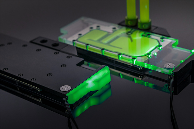
EKWB’s EK-Vector RTX 2080 and EK-Vector RTX 2080 Ti full-cover single-slot water blocks for NVIDIA’s reference design GeForce RTX 2080 and GeForce RTX 2080 Ti add-in-boards come in eight versions, all featuring the company’s cold plate with proprietary Open Split-Flow micro-channels. Traditionally for EKWB, the EK-Vector RTX water blocks use standard G ¼ inch barbs for tubing and are therefore compatible with a wide range of LCS setups. To further improve cooling performance, EKWB will also offer specially designed backplates.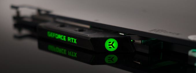
Depending on the version, the cold plate is made of bare electrolytic copper or nickel-plated electrolytic copper, whereas the cover is made of transparent plexiglass or black acetal. Meanwhile, all versions featuring nickel-plated cold plates are also outfitted with RGB strips, which use a 4-pin 12 V connector and can be controlled by RGB command software from the leading motherboard brands (ASUS, ASRock, GIGABYTE, MSI).
As is typically the case, custom liquid cooling does not come cheap. EKWB’s EK-Vector RTX GPU water blocks will retail for €129.9 – €149.9 depending on the specific SKU, whereas the backplates will cost €39.9 – €43.9. EKWB will start shipments of its water blocks on September 20, whereas backplates will hit the market in October.
EKWB's GPU Water Blocks for NVIDIA's GeForce RTX Cards SKU Price in EUR
with 22% VATPrice in USD
with 22% VATPrice in USD w/o VAT EK-Vector RTX 2080 Ti – Copper + Plexi €129.90 $151 $124 EK-Vector RTX 2080 Ti – Copper + Acetal €129.90 $151 $124 EK-Vector RTX 2080 Ti RGB – Nickel + Plexi €149.90 $174 $142 EK-Vector RTX 2080 Ti RGB – Nickel + Acetal €144.90 $168 $138 EK-Vector RTX 2080 – Copper + Plexi €129.90 $151 $124 EK-Vector RTX 2080 – Copper + Acetal €129.90 $151 $124 EK-Vector RTX 2080 RGB – Nickel + Plexi €149.90 $174 $142 EK-Vector RTX 2080 RGB – Nickel + Acetal €144.90 $168 $138 EK-Vector RTX Backplate – Black €36.90 $43 $35 EK-Vector RTX Backplate – Nickel €43.90 $51 $42 Related Reading:
- Turing Custom: A Quick Look At Upcoming GeForce RTX 2080 Ti & 2080 Cards
- NVIDIA Teases GeForce RTX 2080 Performance Numbers, Announces Ansel RTX
- NVIDIA Announces the GeForce RTX 20 Series: RTX 2080 Ti & 2080 on Sept. 20th, RTX 2070 in October
More...
-
09-07-18, 08:20 AM #8606
Anandtech: The SteelSeries Apex M750 Mechanical Gaming Keyboard Review: Set Apart by
Today we are taking a look at the SteelSeries Apex M750, the highest-end mechanical keyboard that SteelSeries currently offers. The Apex M750 also sports the company's new QX2 mechanical switches, which we will also examine closely in this review.
More...
-
09-07-18, 09:30 AM #8607
Anandtech: Philips Preps 499P9H Curved 49-Inch 5K Display with USB-C Docking & Webcam
Last week at IFA, Philips demonstrated its upcoming ultra-wide curved 49-inch monitor. The new 499P9H display features a 5K resolution with a 32:9 apect ratio, and will be aimed at various B2B clients that normally use two LCDs. Among key selling points of the new monitor – besides its sheer size – are a pop-up webcam, a USB Type-C docking, and a GbE controller.
A number of display suppliers have introduced their 49-inch ultra-wide LCDs featuring a 32:9 aspect ratio and a 3840 × 1080 resolution over the past few quarters. The displays are based on a Samsung panel and target various applications, including business/productivity and gaming. Philips was first to launch its ultra-wide 492P8 monitor after Samsung released its 49-inchers last year, so it is not surprising that it will be among the first third-party companies to adopt Samsung’s 5K ultra-wide VA panel that we're unofficially hearing is expected to hit mass production this month.
The Philips 499P9H offers a 5120 × 1440 resolution, which is called DQHD (dual quad HD), and is designed to substitute two 27-inch 2560 × 1440 monitors. Based on what we know about this panel unofficially, it has a 1800R curvature and supports refresh rates up to 120 Hz. B2B monitors featuring the panel will likely support a 60 Hz refresh rate, whereas their gaming counterparts will likely gain AMD’s FreeSync technology and a dynamic refresh rate between 48 Hz and 120 Hz (or 30 Hz and 120 Hz). Meanwhile, since we are dealing with a VA panel, expect a high contrast ratio along with 178º/178º vertical/horizontal viewing angles.
One of the important features of the Philips 499P9H monitor is its pop-up Windows Hello-compatible webcam, which will likely be welcome by various business and enterprise users who require a biometric authentication.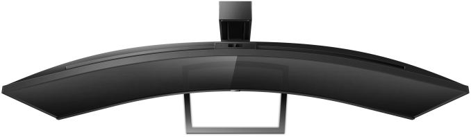
Since the Philips 499P9H has to be compatible with a wide variety of PCs, it features not only a USB Type-C connector with docking and power delivery capabilities, but also a more traditional DisplayPort 1.2 input and two HDMI 2.0 ports. Like other large displays, the 499P9H naturally supports picture-by-picture (PBP) and picture-in-picture (PiP) modes as such LCDs are usually used with multiple PCs at once. In addition, the monitor has a dual-port USB 3.0 hub as well as an Ethernet connector to provide a GbE connectivity to Apple’s MacBooks and other laptops that only feature USB Type-C headers.
Philips did not touch upon the ETA nor MSRP of its upcoming 499P9H display at the trade show. Since Samsung yet has to kick off mass production of the panel and start using it itself, expect the 499P9H to arrive sometimes in 2019. Keep in mind that since the 499P9H is aimed primarily at B2B clients, it may not be readily available from the usual retailers.
Related Reading:Philips Ultra-Wide 49-Inch Displays 499P9H 492P8 Panel 49" VA Native Resolution 5120 × 1440 3840 × 1080 Maximum Refresh Rate ? 60 Hz Response Time unknown unknown Brightness high up to 600 cd/m² (?) Contrast high up to 5000:1 (?) Backlighting LED Viewing Angles 178°/178° horizontal/vertical Curvature 1800R Aspect Ratio 32:9 (3.56:1) Color Gamut sRGB (?) sRGB Dynamic Refresh Rate Tech unknown unknown Pixel Pitch 0.234 mm² 0.312 mm² Pixel Density 108 PPI 81.41 PPI Inputs 1 × DisplayPort 1.2
1 × USB Type-C
2 × HDMI 2.01 × DisplayPort 1.2
1 × D-Sub
2 × HDMIAudio 3.5 mm input and output USB Hub 2 × USB 3.0 Type-A connectors Ethernet 1 GbE port MSRP unknown unknown
- Philips Readies Curved Ultra-Wide 492P8 Display: 49”, 32:9, USB-C, Sub-$1100
- MSI Optix MAG491C Hands-On: A 49-Inch 32:9 LCD with FreeSync
- ASUS Launches VG49V: An Ultrawide Curved 32:9 49-Inch FreeSync LCD
- Samsung Announces First Freesync 2 Monitors: CHG70 & CHG90 - Quantum Dots, Up to 49”, 144 Hz, DCI-P3
- ASUS Demonstrates ProArt PA34V Professional Curved UWQHD Display with TB3
- Samsung Unveils CJ79 & CJ89 Curved LCDs: Quantum Dots, TB3 & USB-C
- JapanNext Launches 35-Inch "UWHD" Curved LCD: AMVA & 200Hz Refresh w/FreeSync
More...
-
09-07-18, 10:35 AM #8608
Anandtech: Toshiba Unveils MG07SCA 12 TB & 14 TB Enterprise-Class HDDs with Dual-Port
Toshiba is announcing that it has started sampling of its latest MG07SCA-series enterprise-class helium-filled hard drives. Notable for utilizing a dual-port SAS interface, the HDDs are aimed at business-critical servers and are rated for 550 TB per year workloads.
Toshiba’s MG07SCA lineup of enterprise-grade hard drive includes two SKUs at 12 TB and 14 TB respectively. The flagship 14 TB model relies on nine PMR platters from Showa Denko with ~1.56 TB capacity each, whereas the 12 TB model relies on eight platters. Both HDDs feature a 7200 RPM spindle speed, a 256 MB cache buffer, and a dual-port SAS 12 Gbps interface. Just like their SATA brethren, the new SAS hard drives are based on Toshiba’s latest-gen helium-filled platform for business-critical HDDs with all the possible enhancements to improve reliability and durability, including top and bottom attached motors, RVFF, environmental sensors, and so on.
The MG07SCA-series HDDs also support Toshiba’s proprietary feature for enterprise-grade hard drives — a persistent write cache (PWC) with power loss protection (PLP), which is particularly important for 4K sector drives that emulate 512B sectors. The PWC with PLP capability protects data in case of power loss while performing read-modify-write (RMW) operation to align the source write request with the physical sectors it has to modify.
When it comes to performance, the MG07SCA drives offer exactly the same specs as their SATA counterparts. The top-of-the-range 14 TB HDD is speced for a 260 MB/s maximum sustained transfer rate, whereas the 12 TB model is slightly slower at around 250 MB/s. Toshiba says that the new SAS hard drives can perform up to 167 read IOPS, and, up to 70 write IOPS (4 KB blocks) when subject to random accesses. As for power, the HDDs consume up to 7.8 W – 8.28 W during random reads and writes depending on the model.
As noted above, Toshiba’s MG07SCA HDDs are aimed at business-critical workloads and are therefore rated for 550 TB average annualized workload, 2.5 million hours MTBF, and are covered with a standard five-year warranty.
Toshiba did not reveal prices of its MG07SCA-series hard drives or when its direct customers intend to start offering them to end users (i.e., operators of datacenters). In general, pricing of such drives depends on the volume ordered, whereas qualification of HDDs for business-critical applications usually takes from months to quarters depending on various factors.Brief Specifications of Toshiba's MG07SCA HDDs Capacity 14 TB 12 TB P/N 4Kn MG07SCA14TA MG07SCA12TA 4Kn SIE MG07SCA14TAY MG07SCA12TAY 512e MG07SCA14TE MG07SCA12TE 512e SIE MG07SCA14TEY MG07SCA12TEY Platters 9 8 Heads 18 16 Recording Technology Perpendicular Magnetic Recording (PMR) / Conventional RPM 7200 RPM Interface SATA 6 Gbps DRAM Cache 256 MB Persistent Write Cache Yes Helium-Filling Yes Sequential Data Transfer Rate (host to/from drive) 260 MB/s ~250 MB/s MTBF 2.5 million Rated Annual Workload 550 TB Acoustics (Active Idle) 20 dB Power Consumption Random read/write 8.28 W 7.8 W Idle 4.73 W 4.36 W Warranty 5 Years
Related Reading: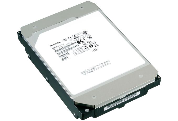
- Toshiba Unveils MN07 Series HDDs Featuring 12 TB & 14 TB Capacity
- Toshiba’s 14 TB HDDs Now Available from Supermicro
- Toshiba Announces 14 TB PMR MG07ACA HDD: 9 Platters, Helium-Filled, 260 MB/s
- Toshiba Samples AL15SE HDDs: Up to 2.4 TB, 10K RPM, SAS
- Toshiba Launches S300 and V300 HDDs for Surveillance and Video Applications
- Toshiba Launches MN06ACA 10 TB HDD for NAS: 7 Platters, Up to 249 MB/s
More...
-
09-07-18, 12:31 PM #8609
Anandtech: Acer Shows Off Triton 900: 17-Inch Convertible Gaming Laptop
Acer last week demonstrated its upcoming ultra-high-end convertible gaming laptop. The Predator Triton 900 notebook is the first high-end mobile PC that uses a convertible form-factor; previously Acer only experimented with entry-level and mid-range convertible gaming laptops.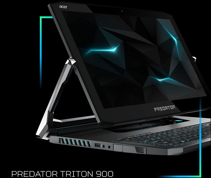
The Acer Predator Triton 900 comes with a 17-inch display featuring an Ultra-HD (3840×2160) resolution that supports NVIDIA’s G-Sync dynamic refresh rate, but the manufacturer does not disclose ranges of the latter. The LCD is attached to a CNC-machined hinge that can flip it into various modes, including laptop and tablet.
Just like its predecessor, the Predator Triton 700, the new notebook places its programmable mechanical keyboard in a rather unorthodox location in order to enable better cooling for high-TDP components while retaining a relatively low z-height. Meanwhile, the laptop’s trackpad can be flipped and transformed into a numpad. Speaking of cooling, it's worth noting that the new Predator Triton 900 is outfitted with Acer’s fourth-generation cooling system featuring Aeroblade 3D fans made of metal, which can generate up to 3.8 CFM of air flow, and which the manufacturer says can offer better cooling performance than traditional coolers.
Acer does not disclose which processor and graphics chips it will be using inside the Predator Triton 900, but considering all the efforts with the form-factor and cooling, it is safe to say that the notebook will pack something like Intel’s Core i7/i9 with overclocking capability along with an NVIDIA’s GeForce GPU.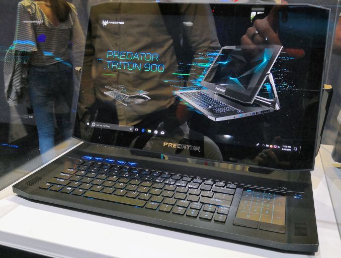
As for connectivity, the Predator Triton 900 looks pretty standard. Besides usual Wi-Fi + Bluetooth on the wireless side of things, the laptop has one Thunderbolt 3 port, one USB Type-C header, two USB 3.0 Type-A connectors, two display outputs (HDMI and a DisplayPort), Gigabit Ethernet, and two 3.5-mm audio jacks. There is also a mysterious bay on the left side of the laptop that could be a compartment for a 2.5-inch storage device or an add-on card, but we cannot confirm the nature of this bay just now.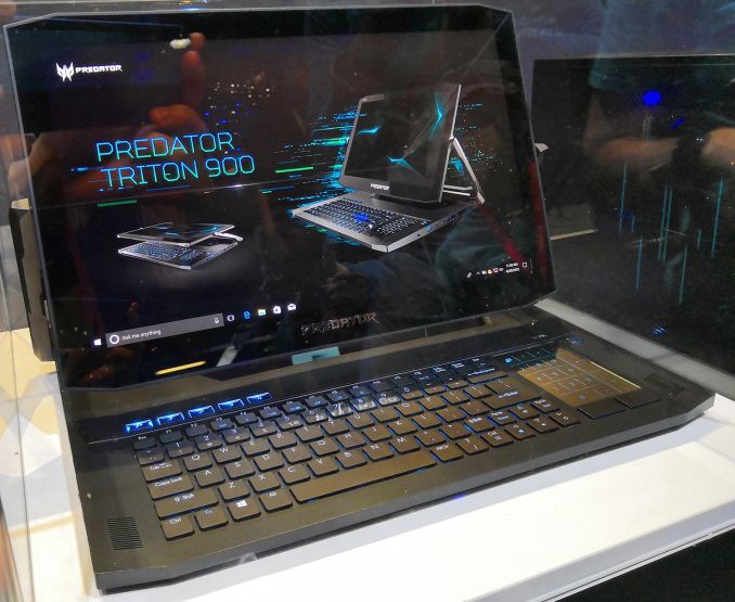
Acer did not disclose price or availability timeframe for its Predator Triton 900 notebook. Typically, companies tend to release products they demonstrate at IFA towards holiday season in the U.S. Meanwhile, considering the fact that the 17-inch convertible gaming laptop is a very special product that may require additional work and Acer’s history of showing early prototypes at IFA, the Predator Triton 900 may not hit retail until sometime in 2019.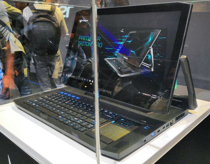
Related Reading:
- Acer Announces Predator Triton 700 Gaming Laptop: Core i7, GeForce GTX 10 Series, & 1 TB SSD
- Acer Predator 21 X Laptop with Curved Display Now Available, Only 300 to Be Made
- Acer Announces Nitro 5 Spin 15.6" Gaming Convertible: 8th Gen Core i7, GeForce GTX 1050
- Acer Announces Switch 7 Black Edition 2-in-1: Core i7, GeForce MX150, TB3, Fanless
- Acer Predator 21 X Laptop with Curved Display Now Available, Only 300 to Be Made
- Acer Unleashes Predator Helios 500 Gaming Notebook: Up to Core i9+, GTX 1070
- Acer Predator Helios 300 SE: White and Gold Gaming Laptop
- Acer Announces The Acer Predator 21 X: 21-Inch Curved Screen Gaming Notebook
More...
-
09-07-18, 03:56 PM #8610
Anandtech: Phison: PS5012-E12 Controller in Mass Production, 20+ SSDs Incoming
Phison and its partners have been absent from the high-end SSD market in the past couple of years. This is partly because its memory supplier, Toshiba, was somewhat late with its SSD-grade 3D NAND memory, but also partly due to its own product planning. Looking to put an end to this absence, this week the company has announced that it has initiated mass production and shipments of its latest PS5012-E12 controller, which is expected to bring Phison and its allies back to the high-end market segment.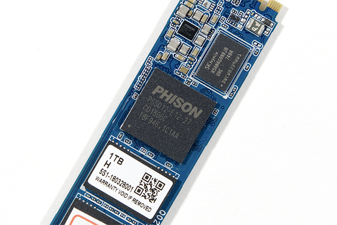
The Phison PS5012-E12 controller features eight NAND channels with 32 CE targets, a DDR4/DDR3L interface for DRAM caching, and a PCIe 3.0 x4 interface. As for features, the chip supports the NVMe 1.3 protocol, LDPC-based error correction, a variety of encryption methods (AES-256, TCG Opal, TCG Pyrite), and a number of proprietary technologies to improve reliability and durability of SSDs. Notably, the controller is made using a 28 nm manufacturing technology, which is a very advanced fabrication process for SSD processors. This should ensure that it packs enough compute horsepower for proper ECC and signal processing when working with modern 3D TLC and 3D QLC NAND memory.
Phison will offer three versions of the PS5012-E12 controller: the original one for high-end client SSDs, the PS5012-E12C with a reduced number of channels and CE targets for mid-range drives, and the PS5012-E12DC for enterprise drives with some additional performance and feature set enhancements.
Speaking of performance, Phison promises that high-end SSDs based on the PS5012-E12 will offer up to 3450 MB/s sequential read speeds, up to 3150 MB/s sequential write speeds, as well as up to 600K random read/write IOPS.
Phison says that its partners have started development of over 20 projects based on the PS5012-E12, but does not disclose whether this includes the cheaper and datacenter variations of the controller. Keeping in mind that the chip is in volume production and Toshiba’s 64-layer 3D TLC NAND is readily available, expect drives based on the PS5012-E12 to hit the market in the coming months.
So far, Patriot and MyDigitalSSD have confirmed plans to use Phison’s PS5012-E12 controller, with the latter already taking pre-orders for the BPX Pro. In the meantime, Phison has a long list of partners who currently offer higher-end, mid-range, and entry-level SSDs powered by Phison’s controllers, including Corsair, GIGABYTE, Kingston, Lite-On, TEKQ, Team Group, Toshiba, Palit (Galax, KFA2, etc.), PNY, ZOTAC, and so on.
MyDigitalSSD plans to start shipping the BPX Pro within a few weeks, and they are currently taking pre-orders. They are often one of the first to ship Phison's new controllers and have historically offered some of the best prices with drives like the original BPX and the more recent SBX. Most Phison E12 consumer drives will probably feature specs similar to the BPX Pro, though later drives may move to Toshiba's 96-layer 3D NAND:Phison NVMe SSD Controller Comparison Controller E12 E12C E8 E8T E7 Model Number PS5012-E12 PS5012-E12C PS5008-E8 PS5008-E8T PS5007-E7 Host Interface PCIe 3.0 x4 PCIe 3.0 x4 PCIe 3.0 x2 PCIe 3.0 x2 PCIe 3.0 x4 Protocol NVMe 1.3 NVMe 1.2 NVMe 1.1b NAND Channels 8 4 4 4 8 NAND Chip Enable lines 32 16 32 32 64 Typical NAND 3D TLC, 3D QLC 64L 3D TLC 15nm MLC Max Capacity 8 TB 2 TB 2 TB 1 TB 2 TB DRAM Support DDR4, DDR3L DDR3(L) None (HMB) DDR3(L) Error Correction LDPC, StrongECC StrongECC BCH Manufacturing Process TSMC 28nm UMC 40nm TSMC 28nm Sequential Read 3200 MB/s 1700 MB/s 1600 MB/s 1600 MB/s 2600 MB/s Sequential Write 3000 MB/s 1700 MB/s 1300 MB/s 1300 MB/s 1300 MB/s 4KB Random Read 600k IOPS 340k IOPS 240k IOPS 120k IOPS 300k IOPS 4KB Random Write 600k IOPS 400k IOPS 220k IOPS 130k IOPS 200k IOPS Retail SSD Availability Soon ? Q4 2017 ? Q1 2016
Related Reading:MyDigitalSSD BPX Pro Specifications Capacity 240 GB 480 GB 960 GB 1920 GB Controller Phison PS5012-E12 NAND Flash Toshiba 64-layer BiCS3 3D TLC Form-Factor, Interface PCIe 3.1 x4, single-sided M.2 2280 Sequential Read 3.4 GB/s 3.4 GB/s 3.4 GB/s 3.4 GB/s Sequential Write 1.1 GB/s 2.1 GB/s 3.1 GB/s 3.1 GB/s Random Read IOPS (QD1) 50 MB/s 55 MB/s 55 MB/s 55 MB/s Random Write IOPS (QD1) 315 MB/s 325 MB/s 325 MB/s 325 MB/s Idle Power Consumption < 900 mW PCIe L1.2 Idle < 2 mW Pseudo-SLC Caching Yes DRAM Buffer Yes TCG Opal Encryption Yes Warranty 5 years Write Endurance 380 TB
0.9 DWPD800 TB
0.9 DWPD1665 TB
0.9 DWPD3115 TB
0.9 DWPDPre-Order Price $92.77 (39¢/GB) $138.55 (29¢/GB) $263.17 (27¢/GB) $563.63 (29¢/GB)
- The Phison E12 Reference Design Preview: A Next-Gen NVMe SSD Controller
- Patriot Demos Viper M.2 SSDs with Phison E12, Up to 2 TB
- The Kingston A1000 NVMe SSD Review: Phison E8 Revisited
- Patriot Readies Viper SSDs With Phison E12 And S12
- The MyDigitalSSD SBX SSD Review: NVMe On The Cheap
- GIGABYTE Launches Its First SSDs: Phison PS3110 S10 with Toshiba’s 3D TLC
Source: Phison
More...


 Quote
QuoteThread Information
Users Browsing this Thread
There are currently 37 users browsing this thread. (0 members and 37 guests)


Bookmarks