

Results 9,751 to 9,760 of 12094
Thread: Anandtech News
-
08-06-19, 03:38 PM #9751
Anandtech: Samsung Unveils 6th Generation V-NAND Memory with Up to 136 Layers
Samsung on Tuesday introduced its sixth-generation V-NAND memory with over 100 active layers. To make V-NAND with over 100 layers viable from performance point of view, the company had to use new circuit design technology. The new memory features 10% lower latencies and consumes 15% lower amount of power when compared to previous-generation V-NAND.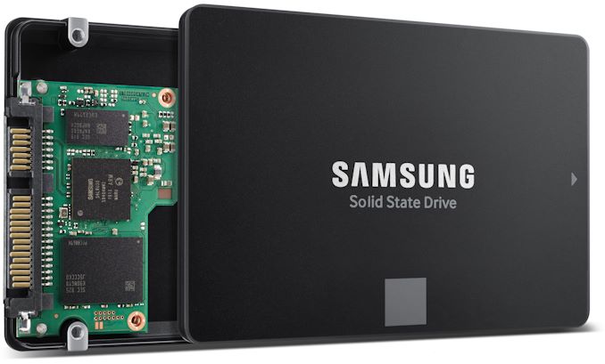
Samsung’s 6th Generation V-NAND features up to 136 layers as well as charge trap flash (CTF) cells. The new memory uses one stack and does not use technologies like string stacking to build over 100 layers. In order to ensure lack of errors and low latencies, Samsung had to use a new speed-optimized circuit design. The latter enabled the new 3D TLC 256 Gb chips to offer below 450 microseconds (μs) latency for write operations and below 45 μs for read operations, which is 10% faster when compared to 5th Generation V-NAND, according to Samsung. Meanwhile, the latest V-NAND also features lower power consumption than its predecessors.
It is noteworthy that the new 256 Gb 136-layer V-NAND devices use 670 million holes, down from 930 million holes with the previous generation, which means that the new chips need less process steps and are easier to manufacture. What is important is that Samsung plans to use its 136-layer architecture with speed-optimized circuit design to build V-NAND devices with over 300 layers by mounting three of the current stacks on top of each other (thus tripling a chip’s capacity).
Initially, Samsung will offer 256 Gb 3D TLC 136-layer V-NAND devices that will first be used for Samsung’s 250 GB SSDs. Later this year Samsung intends to release 512 Gb 136-layer V-NAND devices that will be used for other drives as well as eUFS storage solutions.
Speaking of the 256 GB 6th Gen V-NAND SSD, it is important to point out that it uses Samsung’s new controller marked as the S4LR030/S94G4MW2.
Related Reading:
- Samsung Shares SSD Roadmap for QLC NAND And 96-layer 3D NAND
- Samsung's New 512 GB UFS 3.0 Chip for Galaxy Fold, Now in Mass Production
- Samsung Starts Production of 1 TB eUFS 2.1 Storage for Smartphones
- The Samsung 970 EVO Plus (250GB, 1TB) NVMe SSD Review: 96-Layer 3D NAND
Source: Samsung
More...
-
08-06-19, 06:56 PM #9752
Anandtech: Rick Bergman Returns to AMD to Lead Computing & Graphics Business
AMD has announced that Rick Bergman had rejoined the company and will lead its Computing and Graphics business. Mr. Bergman’s focus will be high-performance PCs, gaming and semi-custom businesses. The return of the former executive emphasizes importance of gaming for AMD.
Rick Bergman has a long history with GPU companies. In the late nineties he used to work at S3 Graphics and then joined ATI Technologies in 2001, where he served at various positions until 2006, when ATI was bought by AMD. From 2006 to 2011, he led AMD’s products group where he was responsible both for CPUs and GPUs. In 2011, Mr. Bergman joined Synaptics, where he served as CEO until recently and significantly transformed the company.
Among the highlights of Rick Bergman’s career at AMD are the company’s highly-successful Radeon HD 4000 and HD 5000 families of products, the GCN architecture that was used by the company’s GPUs for years, as well as AMD’s ‘Fusion’ program that enabled the company to integrate its GPUs into its CPUs and eventually create high-performance SoCs for Microsoft’s and Sony’s game consoles.
Rick Bergman is the latest addition to AMD’s graphics and gaming team. Last month AMD hired Frank Azor, a former head of Dell’s Alienware division, to head its gaming-related efforts. Meanwhile, Mr. Bergman brings both general management and semiconductor experience.
Related Reading:
- An Interview with AMD’s Forrest Norrod: Naples, Rome, Milan, & Genoa
- All Ryzen: Q&A with AMD CEO Dr. Lisa Su
- CES 2019 Question and Answer Session with AMD CEO, Dr. Lisa Su
Source: AMD
More...
-
08-06-19, 11:29 PM #9753
Anandtech: Samsung Announces the Exynos 9825 SoC: First 7nm EUV Silicon Chip
This year’s Galaxy S10 has been in a bit of an odd situation: Although Samsung continued to dual-source its SoCs, using both its own Exynos 9820 SoC as well as Qualcomm’s Snapdragon 855, the phone found itself in the unusual situation of pitting 8nm silicon against 7nm silicon from TSMC. So although the new Exynos 9820 did fairly well in testing and improved a lot over the Exynos 9810, the chip seemingly still had disadvantages against the competition when it came to power efficiency, likely linked to its process technology disadvantages. On top of the power efficiency disadvantages, the chip also had a notable die area disadvantage versus the Snapdragon, coming in at 127mm² versus the smaller 73mm² competition.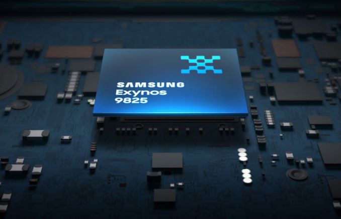
Samsung’s 7nm EUV process node was noted as having started mass production back in October of last year, although we’re not sure exactly which chip this was referring to, and we had hopes that it would be the chip for the S10 but alas it was not to be.
This time around, Samsung is seemingly bridging the gap with the introduction of the new Exynos 9825 – a 7nm LPP refresh of the Exynos 9820.
The new chip very much looks like a die-shrink/mid-cycle refresh with largely the same IP generation as the 9820, still featuring Samsung’s M4 Cheetah cores as well as a Mali-G76 GPU. Samsung also doesn’t seem to have changed the clock frequencies of the chip very much: The M4 cores are still running at a peak frequency of 2.73GHz and the A55 cores also run at 1.95GHz. We do see a bump in the frequencies of the middle cores that goes up from 2.31GHz to 2.4GHz.Samsung Exynos SoCs Specifications SoC Exynos 9820 Exynos 9825 CPU 2x M4 @ 2.73 GHz
2x 512KB pL2
2x Cortex A75 @ 2.31 GHz
2x 256KB pL2
4x Cortex A55 @ 1.95 GHz
No pL2's
Sharedcomplex sL3 @ 4MB
2x M4 @ 2.73 GHz ?
2x Cortex A75 @ 2.4 GHz ?
4x Cortex A55 @ 1.95 GHz ?GPU Mali G76MP12 @ 702 MHz Mali G76MP12 @ ? MHz Memory
Controller4x 16-bit CH
LPDDR4X @ 2093MHz4x 16-bit CH
LPDDR4X @ 2093MHzISP Rear: 22MP
Front: 22MP
Dual: 16MP+16MPRear: 22MP
Front: 22MP
Dual: 16MP+16MPMedia 8K30 & 4K150 encode & decode
H.265/HEVC, H.264, VP98K30 & 4K150 encode & decode
H.265/HEVC, H.264, VP9Integrated Modem Shannon 5000 Integrated LTE
(Category 20/13)
DL = 2000 Mbps
8x20MHz CA, 256-QAM
UL = 316 Mbps
3x20MHz CA, 256-QAMShannon 5000 Integrated LTE
(Category 20/13)
DL = 2000 Mbps
8x20MHz CA, 256-QAM
UL = 316 Mbps
3x20MHz CA, 256-QAMMfc. Process Samsung
8nm LPPSamsung
7nm LPP (EUV)
On the GPU side, Samsung has also stuck with the same GPU configuration as with 9820, using a MP12 configuration of the G76. According to the company the 9825's GPU is clocked hgiher - so it will outperform its predecessor - however the company has yet to disclose specific clockspeeds.
As for the integrated modem, Samsung has retained their Shannon 5000, a Category 20/13 modem. This modem has a peak download rate of 2 Gbps (with 8x carrier aggregration), while uploads top out at 316 Mbps. We had been wondering if Samsung would be able to squeeze in a 5G modem for this SoC, but it looks like it's just a bit too early for that. Instead, 5G can be accomplished by pairing the SoC with Samsung's 5G Exynos Modem 5100.
The new chip is likely to be featured in the new Galaxy Note10 – Samsung will continue to use Snapdragon chips for some markets, and this could be an explanation for the new chip not having that big improvements on the part of the CPU complex as it’s aiming for performance parity with the Snapdragon. We also have to note that Samsung would have to invest the process improvements into improving power efficiency rather than raising performance.
The chip reminds us of the Exynos 5430 from a few years ago which was also a process-shrink to the chip that ended up in the Galaxy S5, representing Samsung’s first 20nm silicon. That chip never ended up in the popular flagship products, but seemingly did serve a purpose as a pipe-cleaner and learning platform for the new process node. The new Exynos 9825 could end up in a similar situation, although being used in the Note10, it won’t nearly have an as long lifespan as we don’t expect it to power the Galaxy S11 next year.
More...
-
08-07-19, 10:24 AM #9754
Anandtech: Sharp to Supply IGZO Displays to Nintendo
In a surprising move, one of Sharp’s top executives revealed that the company will supply its IGZO displays to Nintendo. Usage of IGZO screens promises to reduce power consumption of Nintendo’s game consoles, though it is unclear which model will get a new type of LCD first.
Katsuaki Nomura, an executive vice president of Sharp, told the Wall Street Journal that the company would supply its IGZO displays to Nintendo. The exec did not disclose specifications of the panel or which of Nintendo’s consoles will get IGZO displays first.
The game console maker is about to release a handheld-only version of its Switch game console as well as a new version of the fully-fledged Switch. Both new devices could benefit of Sharp’s IGZO displays because of their lower power consumption and potentially higher image quality, but it remains to be seen whether Nintendo decides to shift both of its upcoming game consoles to a new type of LCDs.
The upcoming versions of Nintendo’s Switch promise considerably longer battery life when compared to existing Switch consoles while using similar batteries. One of the key reasons why the new units feature lower power consumption is believed to be a new SoC from NVIDIA.
Sharp and Nintendo have a long history of working together as the former designed auto stereoscopic display for the latter's 3DS console.
Related Reading:
- Nintendo Announces New Version of Switch with Longer Battery Life
- Update: Nintendo Reveals Handheld-Only Switch Lite, With a New NVIDIA SoC
- Razer Enters The Smartphone Arena With The Razer Phone
- New 8K OLED Displays for Tablets and Laptops: 8.3 and 13.3 Inches
Source: Wall Street Journal
More...
-
08-07-19, 02:21 PM #9755
Anandtech: Western Digital Reveals Ultrastar DC SN340 SSDs for Read Intensive Workloa
Western Digital has introduced its new accelerator drives designed for very read-intensive workloads. The key feature of the Ultrastar DC SN340 Very Read Intensive (VRI) SSDs is their low read latency which is important for write-once read many applications, such as video-on-demand services, distributed databases, and emerging AI/ML workloads.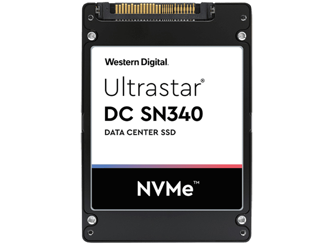
Nowadays video streaming providers use 1 TB SATA SSDs that offer a ratio of IOPS to bandwidth that satisfies their needs in terms of numbers of parallel users/streams (RIOPS). In a bid to optimize power, costs, and the number of racks in their datacenters while still meeting their requirements, VOD services need higher-capacity drives with higher performance and specific functionality. Western Digital believes that VRI SSDs is a type of devices that will satisfy requirements of the aforementioned (and many other read-intensive) workloads.
Carrying 3.84 or 7.68 TB of usable capacity, Western Digital’s Ultrastar DC SN340 U.2 drives optimized for write-once read many workloads are based on the company’s proprietary controller as well as 96-layer BiCS4 3D TLC NAND. With up to 3.3 GB/s sequential read speed, up to 1.5 GB/s write speed, up to 420K random read IOPS, and a 6.5 W maximum power consumption, the Ultrastar DC SN320 are substantially faster and more power efficient than SATA SSDs used by various VOD companies today.
One key thing to note about the Ultrastar DC SN340 is that it requires all requests to be 32 KB aligned to guarantee consistent performance and appropriate endurance, so these drives are not for everyone. This is a result of the drive's Flash Translation Layer (FTL) managing data with a coarser granularity, which significantly reduces the size of the indirection tables and allows the drive to operate with less DRAM than the usual 1GB per 1TB ratio.
In addition to video streaming services, VRI SSDs can be used for other write-once read many applications. Distributed No-SQL Databases (Apache Cassandra, MongoDB, etc.) that sequentially write in append mode and avoid overwrites can benefit from such drives and their low read latency. Furthermore, various AI and ML applications that use training while performing loads of reads also take advantage of VRI drives.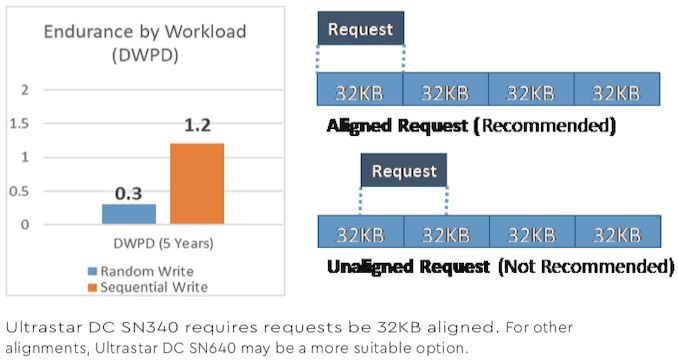
Western Digital does not disclose when it plans to start volume production of its Ultrastar DC SN340 VRI SSDs, but it is logical to assume that when its customers learn how to better use such drives, these products will be made available.Western Digital's Ultrastar DC SN340 SSDs 2.5-Inch
U2Capacities 3,840 GB
7,680 GBInterface PCIe 3.0 x4 (NVMe) Controller Proprietary NAND 96-layer BICS4 3D TLC NAND Sequential Read up to 3300 MB/s Sequential Write up to 1500 MB/s Random Read (4 KB) IOPS up to 420K IOPS Random Write (4 KB) IOPS up to 7K IOPS Mixed Random Read/Write
(max IOPS 70%R/30%W, 4KB)up to 139K IOPS Power Active 6.5 W MTBF 2 million hours Warranty Five years Note: Performance numbers are based on 7.68 TB U.2 SSD
Related Reading:
- HGST Ultrastar SN200 Accelerator: 7.68 TB Capacity, 6.1 GB/s Read Speed, 1.2M IOPS
- Western Digital Starts Shipments of Client SSDs Based on 96-Layer BICS4 3D NAND
- Western Digital: 96-Layer 3D NAND Progressing Well, Shipping to Retail Customers
- Western Digital Begins to Sample QLC BiCS4: 1.33 Tbit 96-Layer 3D NAND
- Western Digital Announces Client NVMe SSDs With New In-House Controllers
- Western Digital: Nearly All NAND Capacities Resumed Normal Operations
Source: Western Digital
More...
-
08-07-19, 02:21 PM #9756
Anandtech: Western Digital Unveils Ultrastar DC SN640 SSDs: Up to 30.72 TB Capacity
Western Digital has announced its new family of enterprise SSDs aimed at mixed-use-case workloads. The new drives use in-house developed components and come in EDSFF E1.L, U.2, and M.2-22110 form-factors offering capacities of up to 30.72 TB.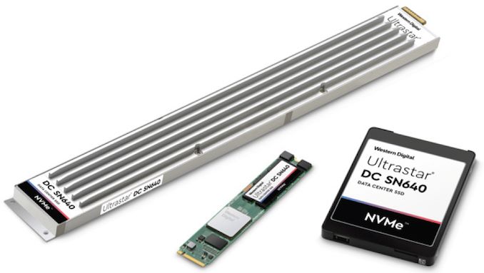
Based on controllers developed by Western Digital internally as well as 96-layer BICS4 3D TLC NAND, the Ultrastar DC SN640 SSDs are aimed at performance-demanding business-critical mixed-workload applications, including SQL Server, MySQL, VMware vSAN, Microsoft Azure Stack HCI solutions, virtual desktops, and other. When it comes to feature set, the drives support power loss protection, AES-256 data encryption, Instant Secure Erase, signed firmware downloads, and other technologies.
Depending on target applications, Western Digital will offer its Ultrastar DC SN640 in three form-factors. For those who need maximum performance and capacity, the manufacturer will offer SSDs in EDSFF E1.L form-factor that will offer capacities of up to 30.72 TB as well as up to 720K random read IOPS. For blade servers running virtual desktops and similar software the maker will offer U.2 SSDs featuring up to 7.68 TB capacities. For space-constrained and OCP environments, the Ultrastar DC SN640 drives will be available in M.2-22110 form-factor as well as capacities of up to 3.84 TB. Considering the workloads, the new SSDs offer tunable endurance of 0.8 or 2 DWPD over five years.
As far as performance is concerned, the Ultrastar DC SN640 6.4 TB U.2 SSD is rated for up to 3.2 GB/s sequential read speeds, up to 2.14 GB/s sequential write speeds, up to 480K random read IOPS, and up to 120K random write IOPS.
Samples of Western Digital’s Ultrastar DC SN640 SSDs are now available to the company’s customers and will ship commercially later.Western Digital's Ultrastar DC SN640 SSDs 2.5-Inch
U2M.2-22110 EDSFF E1.L Capacities 0.8 DWPD 800 GB
1,600 GB
3,200 GB
6,400 GB960 GB
1,600 GB
3,840 GB7.68 TB
15.36 TB
30.72 TB2 DWPD 960 GB
1,920 GB
3,840 GB
7,680 GB- - Interface PCIe 3.0 x4 (NVMe) Controller Proprietary NAND 96-layer BICS4 3D TLC NAND Sequential Read up to 3200 MB/s Sequential Write up to 2140 MB/s Random Read (4 KB) IOPS up to 480K IOPS Random Write (4 KB) IOPS up to 120K IOPS Mixed Random Read/Write
(max IOPS 70%R/30%W, 4KB)up to 240K IOPS Power Active 12 W 8.25 W 20 W Encryption AES-256 Power Loss Protection Yes MTBF 2 million hours Warranty Five years Note: Performance numbers are based on 6.4 TB U.2 SSD
Related Reading:
- Western Digital Starts Shipments of Client SSDs Based on 96-Layer BICS4 3D NAND
- Western Digital: 96-Layer 3D NAND Progressing Well, Shipping to Retail Customers
- Western Digital Begins to Sample QLC BiCS4: 1.33 Tbit 96-Layer 3D NAND
- Western Digital Announces Client NVMe SSDs With New In-House Controllers
- Western Digital: Nearly All NAND Capacities Resumed Normal Operations
Source: Western Digital
More...
-
08-07-19, 05:55 PM #9757
Anandtech: The AMD 2nd Gen EPYC "Rome" Launch Live Blog
The second – and arguably largest – shoe in the Zen 2 launch is dropping today: AMD’s EPYC 7002-series “Rome” processor. Based on all the things that made 3rd gen Ryzen great just a month ago, now AMD is doing it bigger and better. With up to 64 cores, AMD will be striking right at the heart of Intel’s server CPU business; and they just might be able to do it.
More...
-
08-07-19, 05:55 PM #9758
Anandtech: Samsung Announces Galaxy Note10 & Note10+: A Redesign With Feature Dispari
It’s that time of the year again. We’ve made it past the first half of 2019 and all vendors have released their initial flagship devices for the year. Samsung was amongst the first to usher in the new generation with the Galaxy S10, S10+ and S10e, and as has been traditional for many years, it’s now time for a refresh of Samsung’s second flagship lineup - the Galaxy Note. Today Samsung is unveiling two new devices: the new Galaxy Note10 and Note10+, marking a significant departure from its usual Note device formula.
More...
-
08-07-19, 07:52 PM #9759
Anandtech: AMD Rome Second Generation EPYC Review: 2x 64-core Benchmarked
If you examine the CPU industry and ask where the big money is, you have to look at the server and datacenter market. Ever since the Opteron days, AMD's marketshare has been rounded to zero percent, and with its first generation of EPYC processors using its new Zen microarchitecture, that number skipped up a small handful of points, but everyone has been waiting with bated breath for the second swing at the ball. AMD's Rome platform solves the concerns that first gen Naples had, plus this CPU family is designed to do many things: a new CPU microarchitecture on 7nm, offer up to 64 cores, offer 128 lanes of PCIe 4.0, offer 8 memory channels, and offer a unified memory architecture based on chiplets. Today marks the launch of Rome, and we have some of our own data to share on its performance.
More...
-
08-08-19, 10:37 AM #9760
Anandtech: Dells XPS 13 2-in-1 7390 Available: Intels 10th Gen Core CPUs Inside
Being one of Intel’s key partners, Dell is usually among the first PC makers to start selling computers based on the latest processors from the developer. On Thursday the company began to sell its XPS 13 2-in-1 model 7390 convertible laptop that is powered by Intel’s 10th Generation Core processors codenamed Ice Lake.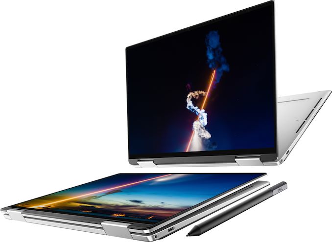
Re-engineered both inside and outside, the latest XPS 13 7390-series 2-in-1 convertibles come in a CNC-machined silver or black aluminum body that features either a fiber composite arctic white woven glass fiber palm rest. The notebooks are equipped with a custom 13.4-inch display panel with InfinityEdge bezels that is 7% larger than on the previous-generation model. The LCD panels feature a 1920×1200 or 3840×2400 resolution, 500 nits brightness, a 1500:1 or 1800:1 contrast ratio, a 16:10 aspect ratio, wide viewing angles as well as Dolby Vision on the FHD+ or 90% DCI-P3 on the UHD+ SKU.
At the heart of the new Dell XPS 13 2-in-1 7390-series convertible notebook are Intel’s 10th Gen Core i3/i5/i7 processors installed onto a more compact motherboard that allowed Dell to make the laptop 7% thinner while making the keyboard and the screen larger. The CPUs are cooled down using a brand-new cooling system that is comprised of two fans, an ultra-thin vapor chamber, and GORE thermal insulation to guarantee consistent performance even under high loads.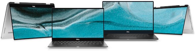
The Ice Lake processors inside the XPS 13 2-in-1 7390-series hybrid notebooks are paired with up to 32 GB of soldered-down LPDDR4X-3733 memory as well as a PCIe SSD of up to 1 TB capacity. As for connectivity, the XPS 13 2-in-1 7390-series features a Killer AX1650 Wi-Fi 6 + Bluetooth controller, two Thunderbolt 3 ports, a microSD card reader, a 3.5-mm jack for headsets, and other options. When it comes to multimedia capabilities, the new convertible has speakers, a microphone array, and a webcam (which is now located on top of the LCD).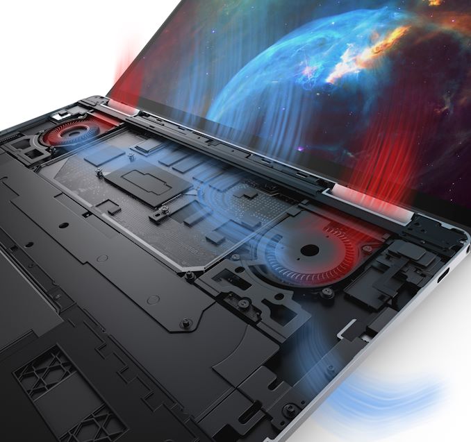
Being very portable, the new laptop features a 7 – 13 mm z-height and weight starting at 1.32 kilograms (2.9 pounds). Meanwhile, the 2019 Dell XPS 13 7390-series 2-in-1 hybrid notebook comes with a 51 Wh battery that promises to last for up to 16 hours (real-world battery life will depend on the usage model, of course).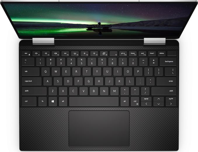
Dell’s XPS 7390-series 2-in-1 convertible notebooks are available starting at $999.99 for an entry-level SKU and going up for higher-end models.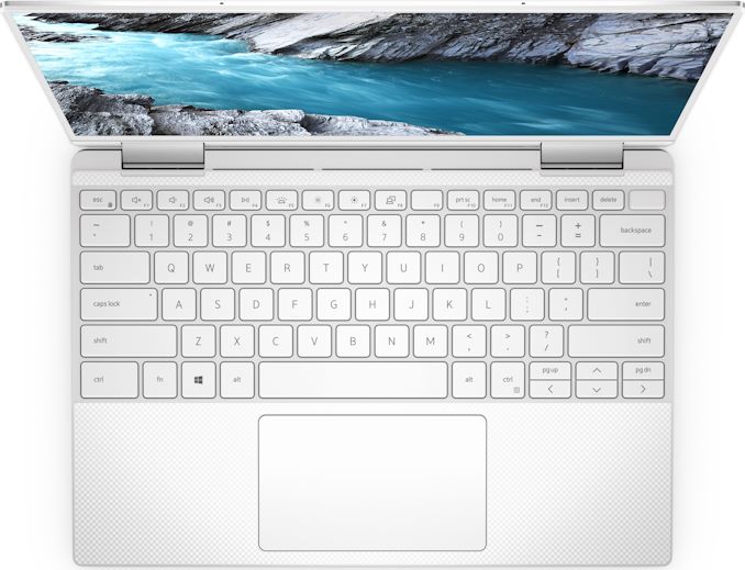
Related Reading:Specifications of the Dell XPS 13 2-in-1 7390 General Specifications LCD Diagonal 13.4-inch Resolution 1920×1200 3840×2400 Brightness 500 cd/m² Contrast Ratio 1800:1 1500:1 Color Gamut ? 100% sRGB
90% DCI-P3Features Dolby Vision HDR HDR400 Touch Support Yes Protective Glass Corning Gorilla Glass 5 CPU Intel’s 10th Gen Core i3
Intel’s 10th Gen Core i5
Intel’s 10th Gen Core i7Graphics Intel's UHD Graphics or Iris Plus GPU RAM 4 GB LPDDR4 SDRAM at 3733 MT/s
8 GB LPDDR4x SDRAM at 3733 MT/s
16 GB LPDDR4x SDRAM at 3733 MT/s
32 GB LPDDR4x SDRAM at 3733 MT/sStorage 256 GB PCIe 3.0 x4 SSD (onboard)
512 GB PCIe 3.0 x4 SSD (onboard)
1 TB PCIe 3.0 x4 SSD (onboard)Wireless Killer AX1650 Wi-Fi 6 + Bluetooth 5.0 (based on Intel's silicon) USB 3.1 2 × TB 3/USB Gen 3.1 Gen 2 Type-C 3.0 - Thunderbolt 2 × TB 3 (for data, charging, DP displays) Cameras Front 720p HD webcam Other I/O Microphone, 2 stereo speakers, audio jack Battery 51 Wh Dimensions Width 29.7 cm | 11.69 inches Depth 20.7 cm | 8.15 inches Thickness 7 - 13 mm | 0.28 - 0.51 inches Weight 1.32 kilograms | 2.9 pounds Launch Price Starting at $999
- The Ice Lake Benchmark Preview: Inside Intel's 10nm
- When Ice Matters: Dell Announces XPS 13 2-in-1 with Ice Lake-U
- Dell Launches XPS 15 7590: Up to 5 GHz and Overclockable, 15.6-Inch OLED
- Dell Refreshes XPS 13 2-in-1: Amber Lake 5W CPUs with Thunderbolt 3
- Dell Releases The XPS 13 2-in-1 Convertible Ultrabook: Infinity Utility
Source: Dell
Gallery: Dells XPS 13 2-in-1 7390 Available: Intels 10th Gen Core CPUs Inside

More...
- The Ice Lake Benchmark Preview: Inside Intel's 10nm


 Quote
QuoteThread Information
Users Browsing this Thread
There are currently 19 users browsing this thread. (0 members and 19 guests)


Bookmarks