

Results 9,761 to 9,770 of 12096
Thread: Anandtech News
-
08-08-19, 10:37 AM #9761
Anandtech: Lenovo Launches ThinkSystem SR635 & SR655 Servers with AMDs EPYC Rome C
Lenovo on Wednesday introduced its first servers based on AMD’s EPYC 7002-series ‘Rome’ processors, which offer up to 64 cores and 128 PCIe 4.0 lanes. The single-socket ThinkSystem SR635 and SR655 machines are designed for a wide variety of applications, including analytics, HPC, virtualized environments and scale-out software-defined storage.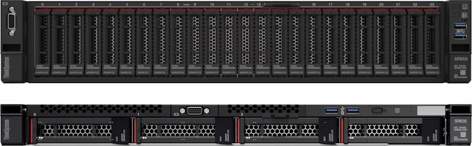
Lenovo’s ThinkSystem SR635 is a 1U server featuring 16 DDR4 DIMMs supporting up to 1 TB of memory using 64 GB RDIMMs, 16 2.5-inch NVMe drives (or four 3.5-inch drives), M.2 boot drives three PCIe 4.0 x16 slots (for three single-wide graphics cards), one PCIe x8 slot, one OCP mezzanine slot, and other I/O capabilities.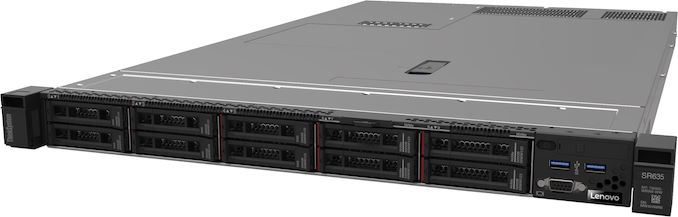
The ThinkSystem SR655 is a larger 2U machine featuring 16 DDR memory slots for 1 TB of DRAM, up to 20 3.5-inch or 32 2.5-inch NVMe storage drives, six PCIe 4.0 slots for single-wide GPUs, an OCP 3.0 connector, and other I/O means.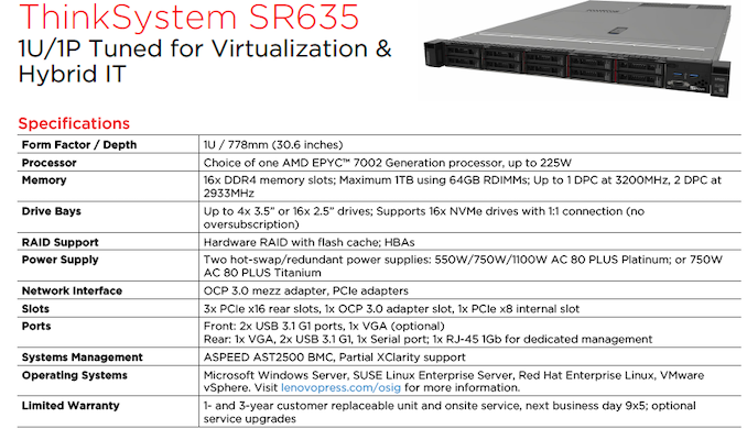
Both ThinkSystem SR635 and ThinkSystem SR655 support hardware RAID flash cache as well as regular set of server connectors along with Aspeed’s AST2500 BMC. Depending on configuration, the machines can be equipped with up to a 1100 W PSU. As for software compatibility, the systems can run Microsoft Windows Server, SUSE Linux Enterprise Server, Red Hat Enterprise Linux, and VMware vSphere.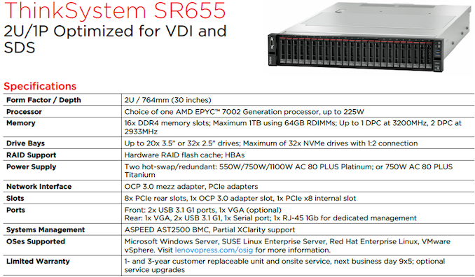
Covered with a one or three-year warranty, the ThinkSystem SR635 and SR655 machines will be available shortly. Prices will depend on configurations of servers.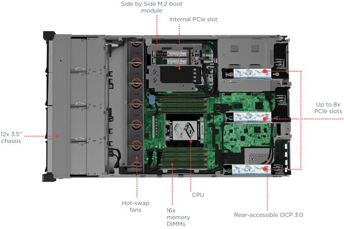
Related Reading: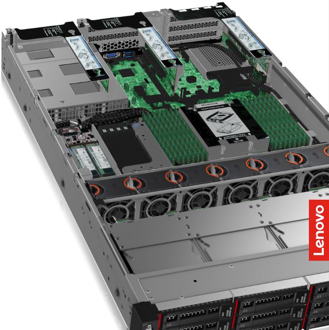
- AMD Rome Second Generation EPYC Review: 2x 64-core Benchmarked
- The AMD 2nd Gen EPYC "Rome" Launch Live Blog
- Lenovo ThinkStation P720 & P920 now with Cascade Lake & Quadro RTX 8000
- Lenovo’s New Cascade Lake ThinkSystem Servers: Up to 8 Sockets with Optane
Source: Lenovo
More...
- AMD Rome Second Generation EPYC Review: 2x 64-core Benchmarked
-
08-09-19, 11:08 AM #9762
Anandtech: Japans Ministry Approves Shipments of Industrial Chemicals to South Korea
Amidst the ongoing trade conflict between Japan and South Korea, there is some good news to close the week out. The Japanese Ministry of Economy, Trade and Industry has approved a new shipment of industrial chemicals to South Korea, which the latter country's high-tech manufacturers rely on for the ongoing production of processors and other components. This is the first of shipment to be approved since early July, when a diplomatic conflict between the two countries broke out. If South Korean manufacturers get the materials on time, it will help to avoid a painful disruption in the manufacturing and shipping of various tech components, including DRAM, NAND flash, LSI chips, and display panels.
Starting as of early July, Japanese producers must now get approval for individual exports to South Korea of polyimides (used both for LCDs and OLEDs), photoresists, and high-purity hydrogen fluoride (used to make chips, such as LSI, DRAM and NAND devices). The major Japanese manufacturers — JSR, Showa Denko (SDK), and Shin-Etsu Chemical — not only control the lion’s share of the global supply for these chemicals, but they also are among the only suppliers that can meet the quality needs that companies like LG, Samsung, and SK Hynix have build their manufacturing lines around.
Export reviews in Japan may take up to three months, whereas South Korean makers typically only keep one to two months' worth of materials in stock because they are highly toxic and uneasy to store. Luckily, the first individual exports was approved by the ministry in about four weeks. The review by the officials concluded that the shipments will not be used for military purposes. However, the ministry did not disclose what specific chemicals are set to ship. Presumably, the South Korean giants will get their needed materials shortly.
Here is what trade minister Hiroshige Seko told local journalists.
“Usually we do not make an announcement when any single export is approved. But in extraordinary circumstances, in which the South Korean government unjustly called our measures an export ban, we decided to make an announcement.”One thing to keep in mind is the starting from July all individual exports from Japan to South Korea will have to be approved separately, which means these shipments will have to pass export review procedures every few weeks.
Related Reading:
- LG Display & SK Hynix Looking to Diversify Industrial Suppliers as Row with Japan Intensifies
- Supply of DRAM, NAND & Displays Could Be Disrupted by Japan & South Korea Dispute
Source: The Japan Times
More...
-
08-09-19, 11:08 AM #9763
Anandtech: Samsung Preps PM1733 PCIe 4.0 Enterprise SSDs For AMD's "Rome" EPYC Proces
With the launch of AMD's new second generation "Rome" EPYC processors, AMD's numerous hardware partners have been lining up to announce their own wares built around the new processors. And this doesn't just go for OEMs and integrators, but it also extends to component suppliers who have been eagerly awaiting the first x86 server processor with PCIe 4.0 support. To that end, yesterday Samsung sent out an announcement confirming that their previously announced PM1733 enterprise SSD supports AMD's new processors, and that just in time for inclusion in Rome systems, they'll be shipping this quarter.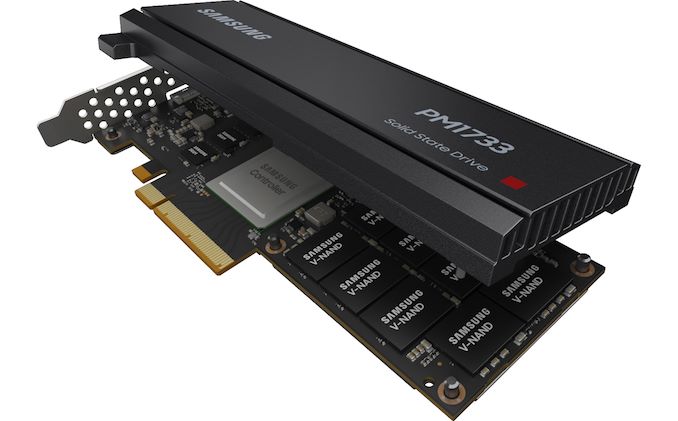
Samsung first announced the PM1733 last fall, as part of its general SSD roadmap update for the then-forthcoming year. The PM1733 is the successor to their PM1723b enterprise SSD, and is designed to take advantage of the bandwidth advances provided by PCIe 4.0. Based on the company’s proprietary controller and paired with 512 Gb 5th Generation V-NAND memory chips, the drive family is rated for read speeds of up to 8 GB/second.
Interestingly, Samsung is offering both PCIe 4.0 x4 and x8 versions of the SSDs, with the U.2 versions using a x4 interface while the alf-length half-height (HHHL) card versions will use x8. The U.2 drives with dual-port capability will offer capacities of up to 30.72 TB, whereas the HHHL cards will carry up to 15.36 TB of useful V-NAND flash.
Overall, Samsung's focus on the drive in terms of specifications is on the drive's read performance rather than its write performance. Along with its 8 GB/sec rated sequential read speed, Samsung says the PM1733 can handle random reads of up to 1500K IOPS, which would make the PM1733 among the fastest drives announced so far.
Samsung will start shipments of its PM1733 SSDs this quarter. Among x86 platforms, the PCIe 4.0 capabilities of the drives will only be available on AMD EPYC 7002 and AMD Ryzen 3000 platforms, but the devices will also work with current PCIe 3.0 platforms from Intel and AMD. The manufacturer has not disclosed prices of the new PM1733 SSDs so far.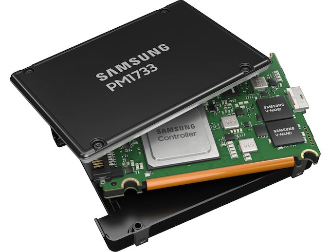
Related Reading:
- Samsung 30.72 TB SSDs: Mass Production of PM1643 Begins
- Samsung Launches Broad Range Of Datacenter SSDs
- Samsung Launches Energy-Efficient PM883 SSD with SATA 3.3, LPDDR4
- Samsung At Flash Memory Summit: 96-Layer V-NAND, MLC Z-NAND, New Interfaces
- Samsung Unveils 6th Generation V-NAND Memory with Up to 136 Layers
- Samsung at Flash Memory Summit: 64-layer V-NAND, Bigger SSDs, Z-SSD
Source: Samsung
More...
-
08-12-19, 09:03 AM #9764
Anandtech: The ASUS Pro WS X570-Ace Review: x8x8x8 with No RGB
Not all motherboards are created equal, and some come with different distinguishing features which amplify them above the others. Whether that be gaming or professional use, the ASUS Pro WS X570-Ace as it stands is the only X570 model which is focused on the professional market with official support for ECC memory, three full-length PCIe 4.0 slots which operate at x16, x8/x8, and is the only current X570 model to operate at x8/x8/x8 across all of its slots, using a full x8 connection from the chipset.
More...
-
08-12-19, 10:54 AM #9765
Anandtech: SK Hynix Announces 3.6 Gbps HBM2E Memory For 2020: 1.8 TB/sec For Next-Gen
SK Hynix this morning has thrown their hat into the ring as the second company to announce memory based on the HBM2E standard. While the company isn’t using any kind of flash name for the memory (ala Samsung’s Flashbolt), the idea is the same: releasing faster and higher density HBM2 memory for the next generation of high-end processors. Hynix’s HBM2E memory will reach up to 3.6 Gbps, which as things currently stand, will make it the fastest HBM2E memory on the market when it ships in 2020.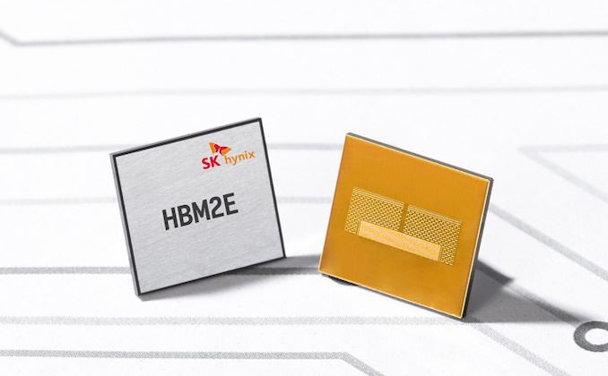
As a quick refresher, HBM2E is a small update to the HBM2 standard to improve its performance, serving as a mid-generational kicker of sorts to allow for higher clockspeeds, higher densities (up to 24GB with 12 layers), and the underlying changes that are required to make those happen. Samsung was the first memory vendor to announce HBM2E memory earlier this year, with their 16GB/stack Flashbolt memory, which runs at up to 3.2 Gbps. At the time, Samsung did not announce a release date, and to the best of our knowledge, mass production still hasn’t begun.
Not to be left behind, SK Hynix is now also readying their own HBM2E memory. In terms of performance, SK Hynix says that their memory will be able to clock at up to 3.6 Gbps/pin, which would give a full 1024-pin stack a total of 460GB/sec of memory bandwidth, and in the process the lead for HBM2E memory speeds. And for more advanced devices which employ multiple stacks (e.g. server GPUs), this means a 4-stack processor could be paired up with as much as 1.84TB/sec of memory bandwidth, a massive amount by any measure. Meanwhile their capacity is doubling, from 8 Gb/layer to 16 Gb/layer, allowing a full 8-Hi stack to reach a total of 16GB. It’s worth noting that the revised HBM2 standard actually allows for 12-Hi stacks, for a total of 24GB/stack, however we’ve yet to see anyone announce memory quite that dense.
Given SK Hynix’s announcement, it’s interesting to note just how quickly HBM2 memory speeds have ramped up here: HBM2 vendors could barely do 1.9 Gbps 24 months ago, and now we’re looking at a near doubling of memory speeds in 3 years. This is a rather significant gain in a short period of time, especially with only a minor revision to the HBM2 spec being required. That said, I remain curious as to how SK Hynix (and Samsung) are going to deal with the heat of an 8-Hi stack running at those clocks; the HBM design philosophy is wide-and-slow, and 3.6 Gbps arguably isn’t so slow.
With their HBM2E memory set to go into mass production in 2020, SK Hynix expects the new memory to be used on “supercomputers, machine learning, and artificial intelligence systems that require the maximum level of memory performance.” All of these are distinctly high-end applications where HBM2 is already being heavily used today, so HBM2E is a natural extension to that market. At the same time, it’s also a reflection of the price/margins that HBM2 carries. HBM2 has remained (stubbornly) high-priced well after its release – a situation that memory manufacturers seem to be perfectly content with – and we’re not expecting HBM2E to change that. So expect to see SK Hynix’s HBM2E memory remain the domain of servers and other high-end equipment.
More...
-
08-12-19, 02:02 PM #9766
Anandtech: Intel Unveils Engineered for Mobile Performance Badge for Project Athena
With the release of the first Ice Lake-U laptops, Intel has announced that there will be a badge/visual identifier for laptops that comply with Intel's Project Athena standard. The ‘Engineered for Mobile Performance’ label will be used for online listings, product pages, on in-store display systems, on packaging, and for demonstrations. Do note, however, that there won't be any ‘Engineered for Mobile Performance’ badges on actual notebooks. Apparently, neither Intel nor PC makers want to put badges on chassis of premium computers (this itself typically being treated as a premium feature).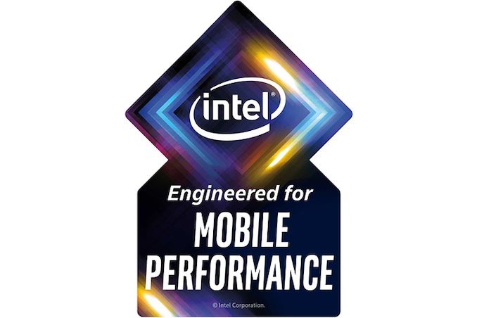
Stylized like a medal, Intel’s ‘Engineered for Mobile Performance’ label indicates that a particular notebook meets Intel’s key experience indicators (KEI) for Athena laptops, which stipulate requirements for performance, features, and battery life, among other things. As previously announced, Intel is doing Athena verification itself, so any product carrying the label means that it has been verified by Intel’s tests and conducted by Intel’s specialists.
With the Athena specifications set to be revised every year, for this first year’s ‘Engineered for Mobile Performance’ notebooks that comply with the Project Athena v1.0 specification, Intel wants the following.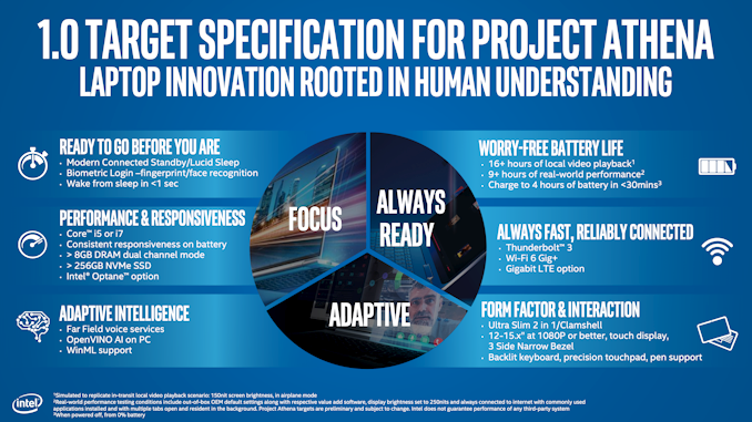
While the PC notebook market is (and will remain) widely varied in features, performance, and prices, Intel is ultimately aiming to tighten up the high-end portion of the market by giving its OEM/ODM partners goals, and matching incentives to reach them. PC hardware in general has been a continual race to the bottom – OEMs are always looking for an edge in costs/price – so in this respect Athena is an effort to entice OEMs to use higher-quality, more expensive (and frequently all-Intel) parts for better performance and greater energy efficiency. Intel is no stranger to this strategy, having employed something similar for both their Centrino and Ultrabook programs, so they are once again turning to it to shape the direction of high-end laptops going into 2020, as well as fending off a push from Arm-based laptops.Intel Project Athena v. 1.0 Requirements Feature Requirement Form-Factor An ultra-thin clamshell or convertible notebook, or a 2-in-1 hybrid PC. Display Touch-enabled 12 – 15-inch display with narrow bezels.
At least a Full-HD resolution.
Stylus supportInternal Hardware Intel’s 10th Gen Core i5 or Core i7 processor with Intel Dynamic Tuning Technology.
At least 8 GB of dual-channel DRAM.
At least a 265 GB NVMe SSD with or without Optane H10 caching SSD.Responsiveness Consistent responsiveness both on battery and on power outlet. Instant Action Connected Standby/Lucid Sleep support.
Wake up from sleep in less than a second.
Wake up to Internet browsing time should not exceed two seconds.Wireless Connectivity Wi-Fi 6 and optional Gigabit LTE. Wired Connectivity Thunderbolt 3. Battery Life At least 9 hours of mixed-workload battery life at 250 nits display brightness.
At least 16 hours of local video playback.
Fast charge support.Intelligence Far Field microphone with voice services.
Hardware-accelerated OpenVINO AI and WinML support (which requires Ice Lake).Interaction Backlit keyboard, precision touchpad, touch display, stylus.
The first laptop to meet Intel’s Project Athena program requirements is Dell’s XPS 13 2-in-1 model 7390 that became available on August 8. Shortly, Acer’s Swift 5, HP’s Envy 13 Wood Series, and Lenovo’s Yoga S940 will also make their debut.
Related Reading:
- Intel's Project Athena: Defining The Next Generation Of Premium Laptops
- Intel Unveils 10th Gen Core Ice Lake-U & Ice Lake-Y Mobile CPUs: 10nm Sunny Cove Later This Year
- Examining Intel's Ice Lake Processors: Taking a Bite of the Sunny Cove Microarchitecture
Source: Intel
More...
-
08-12-19, 07:58 PM #9767
Anandtech: ADATA Expands XPG SX8200 Pro Range with 2 TB Model
Over the past few months we have seen a number of companies announcing high-end 2 TB PCIe 4.0 x4 M.2-2280 SSDs, which was not particularly surprising given positioning of these drives as well as expected lonf lifecycle on the market. What is a bit more surprising is that some manufacturers are also expanding their existing product lineups with 2 TB SSDs as NAND prices continue to fall. One of such companies is ADATA, which has just released a 2 TB flavor of its XPG SX8200 Pro.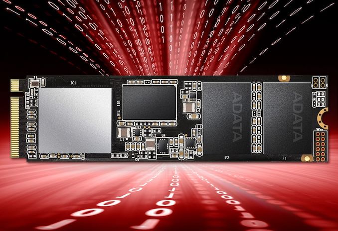
ADATA’s XPG SX8200 Pro is a version of the company’s Gammix S11 Pro without an aluminum heat spreader, which ensures compatibility with laptops. Both drives come in the M.2-2280 form-factor and feature a PCIe 3.0 x4 interface, they are based on Silicon Motion’s SM2262EN controller (eight NAND channels, four ARM Cortex-R5 cores, NVMe 1.3, LDPC ECC, RAID engine, etc.) accompanied by Micron’s 3D TLC NAND. Previously, these drives only featured 256 GB, 512 GB, and 1 TB configurations, but recently ADATA expanded the family with a 2 TB model.
As for performance, the manufacturer claims that the top-of-the-range XPG SX8200 Pro 2 TB drive offers up to 3.5 GB/s sequential read speed and up to 3 GB/s sequential write speed when pSLC caching is used (data based on CDM benchmark), as well as up to 360K random read/write 4K IOPS. The drive is rated for 1280 TB over a 5-year warranty period.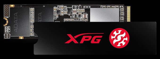
ADATA’s 2 TB XPG SX8200 Pro is already available in the US for $289.99, in select European countries (from eBay) for about €306 ~ €308, and in Japan for ¥36,680.ADATA XPG Gammix S11 Pro Specifications Capacity 256 GB 512 GB 1 TB 2 TB Model Number ASX8200PNP-256GT-C ASX8200PNP-512GT-C ASX8200PNP-1TT-C ASX8200PNP-2TT-C Controller Silicon Motion SM2262EN NAND Flash IMFT 3D TLC NAND Form-Factor, Interface M.2-2280, PCIe 3.0 x4, NVMe 1.3 Sequential Read 3500 MB/s Sequential Write 1200 MB/s 2300 MB/s 3000 MB/s Random Read IOPS 220K IOPS 390K IOPS 360K IOPS Random Write IOPS 290K IOPS 380K IOPS 360K IOPS Pseudo-SLC Caching Supported DRAM Buffer Yes, capacity unknown TCG Opal Encryption No Power Management DevSleep, Slumber (0.14 W). Warranty 5 years MTBF 2,000,000 hours TBW 160 TB 320 TB 640 TB 1280 TB Additional Information Link
Related Reading:
- Comparing Two 1TB NVMe Drives with Same NAND, Same Controller: XPG SX8200 Pro vs HP EX950
- ADATA Announces XPG Gammix S11 Pro: SM2262EN, 3D TLC, Up to 3.5 GB/s
- The Silicon Motion SM2262EN SSD Controller Preview: Good And Bad Amplified
Sources: ADATA, PC Watch
More...
-
08-13-19, 12:49 PM #9768
Anandtech: AMD Quietly Releases Low-End OEM Radeon 600 Series: Radeon Rebadge 2019
While AMD’s focus with the launch of their Radeon RX 5000 series “Navi” product stack has been on midrange desktop cards – and rightfully so – it’s not the only market AMD serves. For as much as the company gets to set their own cadence in hardware design cycles, when it comes to hardware release cycles the company still needs to move to the beat of their single biggest customers: the OEMs. And with the OEMs being driven by market trends and seasonal, cyclical matters, OEMs have historically asked for new hardware between actual design cycles.
To that end, today AMD has quietly announced a new generation of products (of sorts), the Radeon 600 series. Aimed at the low-end of the market – and primarily laptops at that – the Radeon 600 parts are a pure rebadge of AMD’s existing 500 series parts, and are designed to flesh out the very bottom of AMD’s product stack. As is typical for low-end parts, these entries are based on a mix of existing AMD GPUs, using Polaris 12/23, GCN 3 “Topaz”, and GCN 1 “Oland” GPUs depending on the performance class.
Overall, this segment of the market is at the very tail end of AMD’s product stack. So low, in fact, that this is the segment where AMD doesn’t even produce new GPUs, as this is where higher-end integrated GPUs take over and the demand isn’t there for super small discrete GPUs. Hence the hodge-podge mix of GPUs; it’s essentially a collection of AMD’s lowest-end GPUs from a few generations, for the specific customers that need them.
As for the rebadging, this is a semi-annual event driven by OEM product cycles. In short, with the shorter product cycles of OEM systems versus retail channel video cards, OEMs want to advertise the latest components when they refresh and update their systems, even when new GPUs are not available. To which NVIDIA and AMD rebrand, refresh, or otherwise re-designate existing SKUs as new OEM-exclusive parts.
[TABLE="align: center"]
[TR="class: tgrey"]
[TD="colspan: 9, align: center"]AMD OEM Desktop & Mobile Radeon Radeon 600 Series[/TD]
[/TR]
[TR="class: tlblue"]
[TD] [/TD]
[TD="width: 144, colspan: 2, align: center"]Radeon
RX 640[/TD]
[TD="width: 144, align: center"]Radeon
630[/TD]
[TD="width: 144, align: center"]Radeon 625[/TD]
[TD="width: 144, align: center"]Radeon 620[/TD]
[TD="width: 144, align: center"]Radeon 610[/TD]
[/TR]
[TR]
[TD="class: tlgrey"]Base Model[/TD]
[TD="colspan: 2, align: center"]Radeon
550X[/TD]
[TD="align: center"]Radeon
540X[/TD]
[TD="align: center"]Radeon 535[/TD]
[TD="align: center"]Radeon 530[/TD]
[TD="align: center"]Radeon 520[/TD]
[/TR]
[TR]
[TD="class: tlgrey"]Compute Units[/TD]
[TD="align: center"]10
(640 SP)[/TD]
[TD="align: center"]8
(512 SP)[/TD]
[TD="align: center"]8
(512 SP)[/TD]
[TD="align: center"]6
(384 SP)[/TD]
[TD="align: center"]6
(384 SP)[/TD]
[TD="align: center"]5
(320 SP)[/TD]
[/TR]
[TR]
[TD="class: tlgrey"]Texture Units[/TD]
[TD="align: center"]40[/TD]
[TD="align: center"]32[/TD]
[TD="align: center"]32[/TD]
[TD="align: center"]24[/TD]
[TD="align: center"]24[/TD]
[TD="align: center"]20[/TD]
[/TR]
[TR]
[TD="class: tlgrey"]ROPs[/TD]
[TD="colspan: 2, align: center"]16[/TD]
[TD="align: center"]8[/TD]
[TD="align: center"]8[/TD]
[TD="align: center"]8[/TD]
[TD="align: center"]4[/TD]
[/TR]
[TR]
[TD="class: tlgrey"]Boost Clock (up to)[/TD]
[TD="colspan: 2, align: center"]
-
08-13-19, 03:58 PM #9769
Anandtech: Samsung Unveils ISOCELL Bright HMX 108 MP Sensor for Smartphones
Samsung this week has introduced the industry’s first 108 megapixel image sensor for smartphones. The Samsung ISOCELL Bright HMX promises to allow smartphones to take photos comparable to those from DSLR cameras. One of the first handsets to use the new sensor will be a phone from Xiaomi.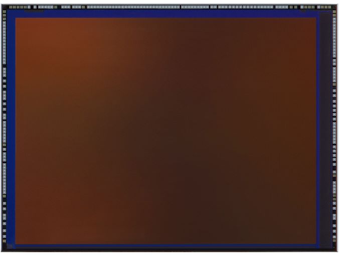
Samsung’s flagship 108 MP ISOCELL Bright HMX is a fairly large 1/1.33-inch image sensor for smartphones. Thanks to the combination of its sheer size and the underlying sensor technology, the Bright HMX is designed to absorb more light than existing image sensors, allowing it to offer better photos even in low-lit conditions. The sensor also supports the company’s 2x2 pixel-binning Tetracell technology, which merges four pixels into one to produce brighter 27 MP photos. In addition, the ISOCELL Bright HMX features Samsung's Smart-ISO capability, which uses high ISOs in darker settings to reduce noise and low ISOs in brighter settings to improve pixel saturation.
When it comes to video, the HMX supports recording at up to 6K (6016 x 3384) resolutions at 30 frames per second, with the same field-of-view as photo mode.
One thing to note is that while the 108 MP ISOCELL Bright HMX sensor can offer a rather high image resolution, it's not a complete system in and of itself. Smartphone manufacturers will need to use SoCs that can handle such a large sensor, both in terms of consuming the sensor's 108 MP output, as well as offering the processing power (ISP and otherwise) to handle all the post-processing expected for a modern smartphone camera.
Samsung plans to begin mass production of the 108 MP ISOCELL Bright HMX image sensor later this month. Meanwhile, Samsung has confirmed that partner Xiaomi will be the first to use the sensor, though the companies are not saying what that first device will be.
Related Reading:
- Samsung Announces Galaxy Note10 & Note10+: A Redesign With Feature Disparity
- Samsung Unveils 64 MP & 48 MP ISOCELL Bright Image Sensors for Smartphones
Source: Samsung
More...
-
08-14-19, 09:21 AM #9770
Anandtech: Acer Launches Predator XN253QX Monitor with 240 Hz & 0.4 ms G2G Response T
Acer has introduced its new Predator XN253QX display, which is aimed at professional gamers who are looking for top-tier response times. The Predator XN253QX has a maximum refresh rate of 240 Hz, features a response time of 0.4 ms, and support NVIDIA’s G-Sync variable refresh rate technology.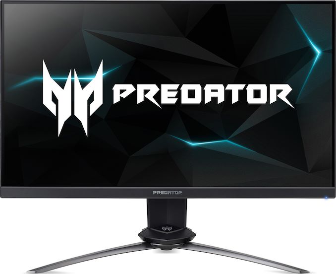
The Acer Predator XN253QX monitor is based on an 8-bit TN panel featuring a 1920x1080 resolution, 400 nits brightness, a 1000:1 contrast ratio, and so on. The key features of the panel are its maximum refresh rate of 240 Hz, a 3 ms native response time as well as a 0.4 ms gray-to-gray response time. Acer notes that the display uses its "Fast Liquid Crystal" technology, but does not really go into detail about what the technology is.
The latest gaming monitor from Acer also supports NVIDIA’s G-Sync variable refresh rate technology with a 30 – 240 Hz range (when operating over DisplayPort), which will certainly please demanding gamers looking for flexibility in their high refresh rate monitors. Like other displays for that market, the Predator XN253QX LCD also has numerous features for gamers, including aim point and dark boost. Last but not least, the display also has an adjustable stand, as well as VESA mounts.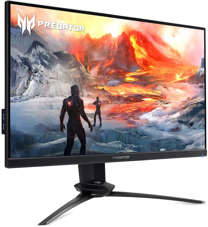
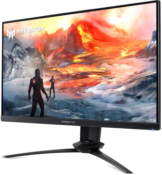
When it comes to connectivity, the Predator XN253QX has a DisplayPort 1.2a as well as HDMI 1.4 connectors. As added bonuses, the LCD also has stereo speakers as well as a USB 3.0 hub.
Acer’s Predator XN253QX will ship in mid-September. In the UK, the product will cost £549, but the price will be different in other regions.Acer's Predator Display with 240 Hz Refresh & 0.4 ms Response Time The Predator XN253QX Panel 25-inch class TN Native Resolution 1920 × 1080 Maximum Refresh Rate 240 Hz Dynamic Refresh Tech NVIDIA G-Sync Range 30 - 240 Hz Brightness 400 cd/m²* Contrast 1000:1 Viewing Angles 170°/160° horizontal/vertical Response Time 0.4 ms GtG Pixel Pitch ~0.28 mm² Pixel Density ~90 PPI Color Gamut Support sRGB (?)
72% NTSCInputs 1×DP 1.2
1×HDMI 1.4Audio 2×2 W speakers
audio input
audio outputVESA Mounts 100 × 100 mm Warranty 3 years Additional Information ? Retail Price in the UK £549 Note *Not all specs of the LCD have been confirmed
Related Reading:
- Acer Unveils KG1 Displays with Sub-1ms Response Time
- AOC’s Agon Monitors with 0.5ms Response Time & 240 Hz Refresh Now Available
Source: Acer
More...


 Quote
QuoteThread Information
Users Browsing this Thread
There are currently 10 users browsing this thread. (0 members and 10 guests)


Bookmarks