

Results 9,931 to 9,940 of 12096
Thread: Anandtech News
-
10-04-19, 03:19 PM #9931
Anandtech: Gen-Z PHY Specification 1.1 Published: Adds PCIe 5.0, Gen-Z 50G Fabric
The Gen-Z Consortium this week released Physical Layer Specification 1.1 for Gen-Z interconnects. The new standard adds enhanced support for PCIe Gen 5 as well as Gen-Z 50G Fabric and Local PHY. The publication of the new PHY revision enables chip developers to implement support for the technologies in upcoming devices featuring Gen-Z interconnects.
Designed to offer high bandwidth and low latency for connections between processors, co-processors/accelerators, and memory/fast storage, Gen-Z 1.0 uses a PCIe physical layer and a modified IEEE 802.3 Ethernet electrical layer standards to provide per-lane speeds of up to the 56 GigaTransfers/second. The Gen-Z 1.0 physical layer specification only defined usage of PCIe Gen 1-4 protocols as well as a 25 GT/s PHY. Thus, to take advantage of all the capabilities of the Gen-Z 1.0 core specification, one needs to comply with the Gen-Z PHY that describes logical, functional, electrical, and channel characteristics for various PHY layers.
The Gen-Z Physical Layer Specification 1.1 defines how to implement a Gen-Z layer capable of operating at PCIe Gen 5 32 GT/s per lane speeds. Revision 1.1 also outlines how to implement a medium to reach a Gen-Z-E-PAM4-50G-Fabric link with a raw data rate of 53.125 GT/s per lane using a 4-level Pulse Amplitude Modulation (PAM4) signaling over the fabric with an ultra-low-latency Phit Forward Error Correction (Phit FEC) encoding using a BCH codeword. Finally, the specification 1.1 describes the implementation of a very short reach Gen-Z-E-PAM4-50G-Local link at 53.125 GT/s per lane using a PAM4 signaling with Forward Error Correction (raw data-rate of 47.222 GT/s).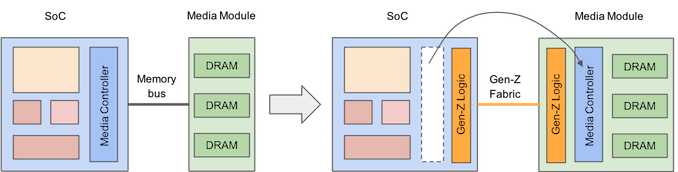
From CPU-memory interface to media-agnostic fabric
In addition to the Physical Layer Specification 1.1, Gen-Z has eight more final specifications and five draft specifications available.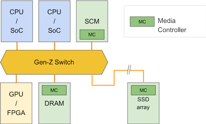
System architecture with Gen-Z
Related Reading- Hot Chips 31 Live Blogs: Gen-Z Chipset for Exascale Fabric
- SMART Modular Shows Off 256 GB Gen-Z Memory Module
- Hot Chips 31 (2019) Programme Announced: Zen, Navi, POWER, Lakefield, Gen-Z, Turing, Lisa Su Keynote
- Gen-Z Interconnect Core Specification 1.0 Published
- Gen-Z Consortium Formed: Developing a New Memory Interconnect
Source: Gen-Z Consortium
Image Source: PLDA
More...
-
10-07-19, 11:21 AM #9932
Anandtech: Intel Xeon W-2200 Family: Cascade Lake-X with ECC and 1TB Support
We recently saw the launch of the consumer Cascade Lake high-end desktop processors last week, featuring up to 18 cores at a low launch price. This week Intel is launching the professional versions of those processors, focused on workstations. The W-2200 family is an upgrade over the older W-2100 family, offering more frequency, more memory support, faster memory support, and a more affordable pricing structure.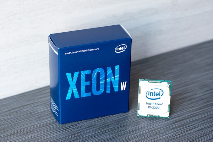
More...
-
10-07-19, 11:21 AM #9933
Anandtech: Intel Announces Price Cut for 9th Generation F and KF Processors
One of the interesting developments of Intel’s 9th Generation Core processors for desktops, known as the S-series, was that the company decided to release versions of the hardware with the graphics disabled in order to use every chip from the wafer. At the time Intel was criticised on its pricing: it was offering the same processor minus graphics for the same bulk unit cost, with no discount. Today Intel is adjusting its strategy, and pricing these F and KF processors lower than before.
More...
-
10-07-19, 03:20 PM #9934
Anandtech: The Modular PC: Intels new Element brings Project Christine to Life
Way back at CES 2014, Razer’s CEO introduced a revolutionary concept design for a PC that had one main backplane and users could insert a CPU, GPU, power supply, storage, and anything else in a modular fashion. Fast forward to 2020, and Intel is aiming to make this idea a reality. Today at a fairly low-key event in London, Intel’s Ed Barkhuysen showcased a new product, known simply as an ‘Element’ – a CPU/DRAM/Storage on a dual-slot PCIe card, with Thunderbolt, Ethernet, Wi-Fi, and USB, designed to slot into a backplane with multiple PCIe slots, and paired with GPUs or other accelerators. Behold, Christine is real, and it’s coming soon.
More...
-
10-07-19, 03:20 PM #9935
Anandtech: Samsung Develops 12-Layer 3D TSV DRAM: Up to 24 GB HBM2
Samsung on Monday said that it had developed the industry’s first 12-layer 3D packaging for DRAM products. The technology uses through silicon vias (TSVs) to create high-capacity HBM memory devices for applications that benefit from high memory bandwidth and capacities, such as higher-end graphics, FPGAs, and compute cards.
Samsung’s 12-layer DRAM KGSDs (known good stack die) will feature 60,000 TSV holes which is why the manufacturer considers its technology one of the most challenging packaging for mass production. Despite increase of the number of layers from eight to 12, thickness of the package will remain at 720 microns, so Samsung’s partners will not have to change anything on their side to use the new technology. It does mean that we're seeing DRAM layers getting thinner, with acceptable yields for high-end products.
One of the first products to use Samsung’s 12-layer DRAM packaging technology will be the company’s 24 GB HBM2 KGSDs that will be mass produced shortly. These devices will allow developers of CPUs, GPUs, and FPGAs to install 48 GB or 96 GB of memory in case of 2048 or 4096-bit buses, respectively. It also allows for 12 GB and 6 GB stacks with less dense configurations.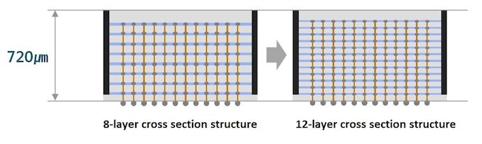
Samsung did not disclose how much will 12-layer 24 GB HBM2 devices cost, but since they will be available exclusively from Samsung, we expect the manufacturer to charge a premium.
Here is what Hong-Joo Baek, executive vice president of TSP (Test & System Package) at Samsung Electronics, had to say:
“Packaging technology that secures all of the intricacies of ultra-performance memory is becoming tremendously important, with the wide variety of new-age applications, such as artificial intelligence (AI) and High Power Computing (HPC). As Moore's law scaling reaches its limit, the role of 3D-TSV technology is expected to become even more critical. We want to be at the forefront of this state-of-the-art chip packaging technology.”Related Reading- Samsung HBM2E ‘Flashbolt’ Memory for GPUs: 16 GB Per Stack, 3.2 Gbps
- JEDEC Updates HBM Spec to Boost Capacity & Performance: 24 GB, 307 GB/s Per Stack
- Samsung Starts Production of HBM2 “Aquabolt” Memory: 8 GB, 2.4 Gbps
Source: Samsung
Gallery: Samsung Develops 12-Layer 3D TSV DRAM Packaging Technology

More...
-
10-08-19, 01:31 PM #9936
Anandtech: TSMC: N7+ EUV Process Technology in High Volume, 6nm (N6) Coming Soon
TSMC announced on Monday that its customers have started shipping products based on chips made by TSMC using its N7+ (2nd Generation 7 nm) process technology that uses extreme ultraviolet lithography (EUVL) for up to four layers. The company also said that its clients are on track to tape out chips to be made using N6 node next year.
When compared to N7 (1st Generation 7 nm) that solely relies on deep ultraviolet lithography, TSMC lists its N7+ process as providing a 15% to 20% higher transistor density as well as 10% lower power consumption at the same complexity and frequency. Furthermore, after less than two quarters in production, TSMC is stating that N7+ now matches N7’s yields, which has been used for over a year now.
Use of EUVL enables TSMC to reduce usage of multipatterning technologies when printing highly complex circuits. This also means that TSMC’s EUV tools can offer output power of greater than 250 watts for day-to-day operations while reaching target goals for availability.
At present, TSMC uses N7+ to produce chips for multiple customers. Two known customers of N7+ are Huawei's Hisilicon with the Kirin 990 5G, and Apple’s A13.Advertised PPA Improvements of New Process Technologies
Data announced by companies during conference calls, press briefings and in press releasesTSMC 16FF+
vs
20SOC10FF
vs
16FF+7FF
vs
16FF+7FF
vs
10FF7FF+
vs
7FF6FF
vs
7FF5FF
vs
7FFPower 60% 40% 60% 50% 70% >37% ~17% 18% 45%
TSMC is on track to start risk production of semiconductors using its N6 process technology in the first quarter of 2020 and initiate high-volume production using this node by the end of next year. TSMC’s N6 is a further development of N7 that offers 18% higher transistor density, uses EUVL for up to five layers and enables designers of chips to re-use the same design ecosystem (e.g., tools, IP, etc.), which lowers development costs. By contrast, N7+ uses different design rules, but also provides more benefits than N6 when compared to N7.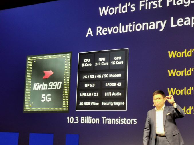
Related Reading- TSMC Announces Performance-Enhanced 7nm & 5nm Process Technologies
- TSMC: Most 7nm Clients Will Transition to 6nm
- TSMC Reveals 6 nm Process Technology: 7 nm with Higher Transistor Density
- TSMC’s 5nm EUV Making Progress: PDK, DRM, EDA Tools, 3rd Party IP Ready
- TSMC: 7nm Now Biggest Share of Revenue
- TSMC: First 7nm EUV Chips Taped Out, 5nm Risk Production in Q2 2019
- TSMC Details 5 nm Process Tech: Aggressive Scaling, But Thin Power and Performance Gains
Source: TSMC
More...
-
10-08-19, 01:31 PM #9937
Anandtech: MSI's Motherboard Refresh for Cascade: Three New Professional X299 Offerin
On the back of Intel's upcoming launch of its HEDT Cascade Lake-X processors in November, MSI has unveiled three new X299 motherboards for content creators, and professional users. The MSI Creator X299, MSI X299 Pro 10G, and the MSI X299 Pro (non-10G) all feature dual Ethernet ports on the rear panel, Realtek ALC1220 HD audio codecs, eight memory slots that support quad-channel DDR4 memory, and also includes USB 3.2 G2 connectivity with ASMedia's ASM3242 USB controller.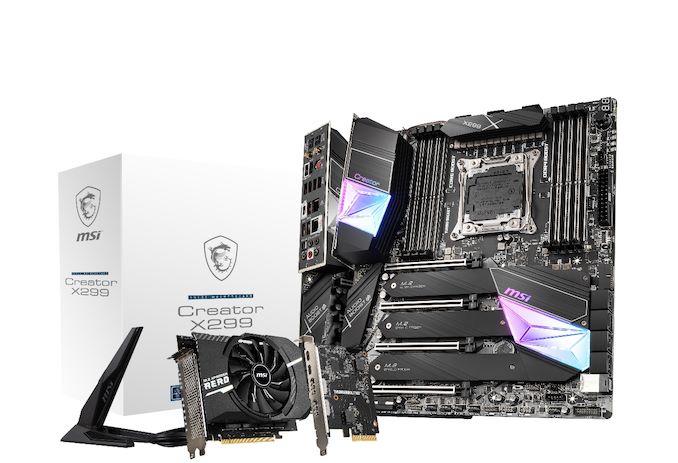
MSI Creator X299
The E-ATX sized MSI Creator X299 model will include plenty of premium features such as an Aquantia AQC107 10 GbE port which is assisted by an Intel I219-V Gigabit NIC providing dual Ethernet ports on the rear, with an Intel AX200 802.11ax wireless interface offering users both Wi-Fi and BT 5.0 connectivity. Focused on content creators and professional users, the Creator X299 allows users the ability to install up to seven PCIe 3.0 x4 M.2 devices; three PCIe 3.0 x4 M.2 slots on the PCB and four with the included MSI M.2 Xpander-Aero add-on card. Other storage options include eight SATA ports and a single PCIe 3.0 x4 U.2 slot for NVMe based storage devices.
A total of eight memory slots with the ability to use DDR4-4266 and install up to 256 GB is present, as well as four full-length PCIe 3.0 slots operating at x16/x8/x8/x8 when used with a 48-lane processor further enhances the board's capabilities. Included in the accessories bundle is a Thunderbolt M3 add-on card which adds dual Type-C and dual DisplayPort 1.4 inputs which further bolsters the appeal of the Creator X299 to content creators and professionals.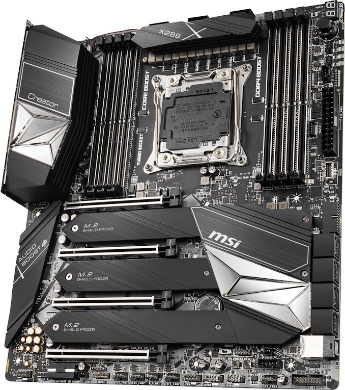
MSI X299 Pro 10G and non-10G
The MSI X299 Pro shifts more onto regular markets with a smaller ATX frame and has a similar networking layout to the Creator X299, but with the 10G coming through a bundled Aquantia AQC107 10 GbE add-on card. This model retains dual Ethernet on the rear panel with one slot controlled by an Intel I1219-V, and the other powered by a Realtek RTL8125-CG 2.5 GbE controller. The X299 Pro 10G has two onboard PCIe 3.0 x4 M.2 slots with room for an additional pair with MSI including an M.2 Xpander-Z dual M.2 slot add-on card in the accessories bundle. This is in addition to six SATA ports which have support for RAID 0, 1, 5, and 10 arrays.
The MSI X299 Pro has support for DDR4-4200 with scope for up to 256 GB across eight available slots and has support for up to quad-channel memory. There are four full-length PCIe 3.0 slots with the second and third slot having just a slot of space between them; an obvious space limitation of its ATX sized frame. The full-length slots operate at x16/x8/x16/x8 when a processor supporting 48-lanes is installed with a clear focus for users to add a Cascade Lake-X processor for maximum support.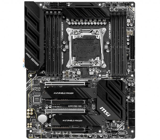
MSI hasn't unveiled specifications on the MSI X299 Pro at present, but it's likely to be similar to the X299 Pro 10G but without the 10G add in card. Availability and pricing information is scarce, but a source indicated that the MSI Creator X299 is set to cost £495 in the UK which represents fantastic value for money with the included Thunderbolt 3 AIC, support for up to seven PCIe 3.0 x4 M.2 slots, and 10 gigabit Ethernet as well. Availability on all three models isn't known, but it is likely that all three models will be available to coincide with the launch of Intel's Cascade Lake-X processors in November.
Related Reading- Intel's Cascade Lake-X CPU for High-End Desktops: 18 cores for Under $1000
- GIGABYTE Unveils Three New 'X299X' Motherboards For Cascade Lake-X
- Intel's X299 Goes Extreme, GIGABYTE X299G Xtreme Waterforce With 10G LAN, 16-Phase VRM
- ASUS Unveils the ROG Rampage VI Extreme Encore X299 Motherboard
- New GIGABYTE X299-WU8 Workstation Motherboard: Dual PLX8747, but Built for Core-X?
- Intel's Next-Generation 'Cascade Lake-X' HEDT CPUs Due in October
More...
-
10-08-19, 05:06 PM #9938
Anandtech: AMD Brings Ryzen 9 3900 and Ryzen 5 3500X To Life
Seemingly always with AMD’s product portfolio, there is a persistent drip of new products being inserted into the product stack throughout the lifetime of a given generation of hardware. Aside from the five Ryzen 3000 series processors launched back in July, we are expecting a new 16-core flagship on top of that list come in November. Until then, AMD has inserted two new processors: one for worldwide consumption, and another for the Chinese OEM market only.
More...
-
10-08-19, 05:06 PM #9939
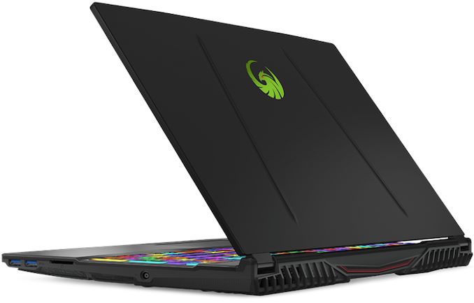
Anandtech: MSIs Alpha 15: AMD Ryzen 3750H and Radeon RX 5500M
MSI is preparing to release a gaming laptop based exclusively on AMD’s CPU and GPU mobile hardware. The Alpha 15 from MSI will be among the first notebooks to use AMD’s latest Radeon RX 5500M GPU.
As the name suggests, MSI’s Alpha 15 is a 15.6-inch class laptop that comes with a Full-HD IPS-class display featuring a 120 Hz, 144 Hz, or 240 Hz refresh rate as well as AMD FreeSync variable refresh, depending on the model. The Alpha 15 weighs 2.3 kilograms and features a 27.5 mm z-height, making it as portable as other gaming notebooks on the market.
MSI’s Alpha 15 notebooks - which the company calls world's first 7nm gaming laptop - will be based on AMD’s Ryzen 7 3000-series mobile CPU family up to four cores, and is accompanied by the Radeon RX 5500M GPU with 4 GB of GDDR6 memory. To cool down the CPU and the GPU, MSI uses a cooling system featuring seven heat pipes as well as two blowers. Depending on exact configuration, the Alpha 15 can be equipped with up to 64 GB of DDR4 memory, one M.2 SSD (with a PCIe 3.0 x4 or SATA interface), and one 2.5-inch SATA hard drive.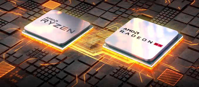
When it comes to connectivity, MSI’s Alpha 15 features Wi-Fi 5, Bluetooth 5.0, a gigabit Ethernet port (a Rivet Networks Killer controller is used in case of premium models), one USB 3.2 Gen 1 Type-C port, three USB 3.2 Gen 1 Type-A connectors, two display outputs (HDMI 2.0, mDP), a card reader (microSD or SD), and 3.5 mm audio connectors. In addition, the system comes with a 720p HD webcam, 2 W stereo speakers co-developed with Giant Speaker, and a backlit keyboard co-designed with Steelseries.
MSI’s Alpha 15 notebooks will come equipped with a 51 Wh battery and a 180 W power brick. The manufacturer does not disclose a proposed battery life.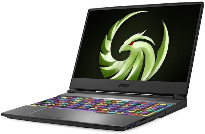
 MSI’s Alpha 15 will be available in the near future. Pricing will depend on exact configurations.
General Specifications of MSI's Alpha 15 laptops Alpha 15 A3DDK Alpha 15 A3DD LCD Diagonal 15.6-inch Resolution 1920×1080 Type IPS VRR AMD FreeSync Refresh Rate 144 Hz
240 Hz120 Hz
144 HzCPU up to AMD Ryzen 7 3750H Graphics Integrated up to AMD Radeon RX Vega 10 Discrete AMD Radeon RX 5500M RAM up to 64 GB DDR4 DRAM Storage SSD 1 × M.2 SSD (SATA or PCIe) HDD 1 × 2.5-inch Card Reader MicroSD Card reader SD Card reader Wireless Wi-Fi 5 + Bluetooth 5.0 USB 1 × USB 3.2 Gen 1 Type-C
3 × USB Gen 3.2 Gen 1 Type-AWired Ethernet GbE Killer GbE Cameras Front 720p HD webcam Other I/O Microphone, 2 stereo speakers, audio jack, microphone in, mDP, HDMI Battery 51 Wh Dimensions Width 357.7 mm Depth 248 mm Thickness 27.5 mm Weight 2.3 kilograms Launch Price ?
Related Reading- MSI’s New Prestige 14 & 15 Laptops Get Intel's Comet Lake-U CPUs & Calibrated 4K Display
- The MSI GE75 Raider Laptop Review: Core i9 and RTX 2080 Performance
- ASUS Launches AMD Ryzen-Based ZenBooks: Two Laptops & a Convertible
- Acer’s Predator Triton 300: Thin Laptop w/ Core i7, GeForce GTX 1650, PowerGem
- Acer Launches 2019 Swift 5: 14-Inch, Ice Lake, GeForce MX 250, 990 Grams
- Razer's Cheaper Blade 15 Base Models: Core i7-9750H, GeForce GTX 1660 Ti, $1599
Sources: MSI
More...
-
10-09-19, 03:31 PM #9940
Anandtech: AMD + ITX + TB3? It's the ASRock X570 Phantom Gaming-ITX/TB3 Motherboard R
When it comes to small form factor systems, options are few and far between. For AMD's X570, out of the 35+ motherboards currently available, just four of them are smaller than mATX. This doesn't give users much to choose from. In this case, mini-ITX implementations have to get it right, and over the last few years ASRock has been at the forefront of the enthusiast small form factor market with an array of models. Today we are reviewing its latest mini-ITX motherboard, the ASRock X570 Phantom Gaming-ITX/TB3. This unique product incorporates Thunderbolt 3 into the frame, pairing it with 802.11ax Wi-Fi 6 as well. Read on for our review.
More...


 Quote
QuoteThread Information
Users Browsing this Thread
There are currently 53 users browsing this thread. (0 members and 53 guests)


Bookmarks