

Results 7,841 to 7,850 of 12096
Thread: Anandtech News
-
02-08-18, 09:36 AM #7841
Anandtech: Patriot Demos Viper M.2 SSDs with Phison E12, Up to 2 TB
In January, Patriot demonstrated its upcoming Viper M.2-branded high-end SSDs. The new drives are powered by Toshiba’s 64-layer BICS 3D NAND flash memory and Phison’s latest PS5012-E12 controller. The drives will hit the market in the upcoming months and will replace Patriot’s Hellfire SSDs.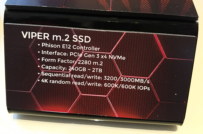
Phison yet has to disclose all the details regarding its new PS5012-E12 controller, but at present we do know that the chip is NVMe 1.3 compliant, it supports 8 NAND channels, it has a PCIe 3.0 x4 interface, and is certified to work with the latest types of 3D NAND memory, including Toshiba’s current-gen 64-layer 3D NAND as well as upcoming flash memory from the company. One of the most prominent features of the PS5012-E12 is its support for stronger ECC algorithms based on LDPC method to handle existing and future NAND with even higher bit densities.
The Patriot Viper M.2 uses Toshiba’s 64-layer BICS3 3D TLC/MLC memory and will be available in various configurations ranging from 240 GB all the way to 2 TB. Patriot demonstrated a 512 GB model of the Viper M.2 at CES, which does not fit into a regular lineup that would include 240, 480, 960 GB and 1920 GB models (if this was the case, the "~2 TB"). We contacted Patriot for a clarification after CES, but we have not received any additional information so far. Perhaps Patriot installs 3D NAND ICs of different capacities to build various Viper M.2 drives, but without any additional information it does not make a lot of sense to make guesses.
When it comes to performance, Patriot republishes Phison’s estimates: up to 3200 MB/s sequential read speed, up to 3000 MB/s sequential write transfers as well as up to 600K 4K random read/write IOPS.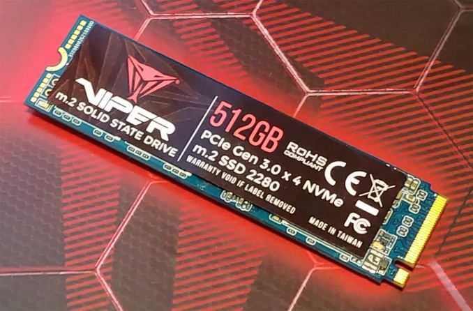
Patriot demonstrated its Viper M.2 drives with the retail sticker on, so we expect the SSDs to become available rather sooner than later (Q1-Q2). With an imminent launch, it might suggest that Patriot is up against the clock regarding tuning the Viper M.2’s firmware to differentiate its drives over the other offerings based on the PS5012-E12. This could be a reason why the company publishes performance numbers released by Phison itself. However, the quicker time to market means more intense competition among high-end SSDs from different manufacturers and this will have an effect on prices that is good for consumers.
Related Reading- Patriot Announces EVLVR Thunderbolt 3 SSD: Phison PS5008-E8, Up to 1.5 GB/s, 1 TB
- Phison at CES 2018: Thunderbolt SSDs, Second-Gen NVMe Controllers
- Patriot Preps Budget-Priced & Phison-Based Scorch NVMe SSD For Q3
- The Patriot Hellfire M.2 480GB Review: Phison NVMe Tested
- Corsair Launches the Neutron NX500 1.6 TB PCIe SSD
- The Corsair Neutron NX500 (400GB) PCIe SSD Review: Big Card, Big Pricetag
More...
-
02-08-18, 10:33 AM #7842
Anandtech: The GlobalFoundries Fab 8 Tour and a Junior Editor's Thoughts
For those who haven’t noticed the anti-contaminant “bunny suit” pictures floating around Twitter, this past weekend Ian and I took part in a tour of GlobalFoundries Fab 8 in Malta, New York. Joining a small media and analyst contingent, we were led behind-the-scenes through the cleanroom and support facilities, and had a chance to speak with select GlobalFoundries executives and managers. There wasn’t a singular purpose or focal point of the tour, and in effect it was more like GlobalFoundries impressing upon us the visceral experience of witnessing their most advanced fab in active operation. This fab, Fab 8, is where GlobalFoundries will create 7nm, with EUV rumbling into motion for them and the rest of the industry.
More...
-
02-08-18, 01:06 PM #7843
Anandtech: SK Hynix Announces SSDs with 72-Layer 3D NAND ICs, Own Controllers
SK Hynix this week has said it has completed development of its enterprise-grade SSDs based on its 512 Gb 72-layer 3D TLC NAND chips as well as its own controllers and firmware. The drives will be available with SATA and PCIe interfaces and will target various applications. Select clients of SK Hynix have already received samples of its eSSDs.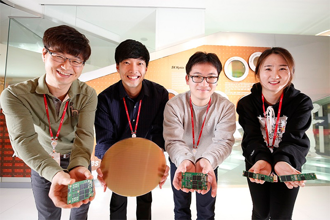
SK Hynix’s SATA SSDs are based on the company’s 72-layer 3D NAND 512 Gb chips, and are designed to offer up to 4 TB of raw NAND flash memory. These drives are rated to support sequential read and write speeds of up to 560 MB/s and 515 MB/s respectively. When it comes to random performance, these drives are capable of up to 98K random read IOPS and up to 32K random write IOPS (but SK Hynix does not disclose queue depth and other factors).
As for SK Hynix’s PCIe-based drives, they come in an M.2 form-factor and offer capacities of 1 TB or higher. The manufacturer declares sequential read performance of up to 2.7 GB/s, sequential write performance of up to 1.1 GB/s, random read performance of up to 230K IOPS as well as random write performance of up to 35K IOPS. SK Hynix does not disclose feature set, but based on their images we can expect them to offer power loss protection.
SK Hynix began production of 72-layer 3D NAND (3D-V4) 512 Gb chips, we believe, in the fourth quarter of 2017, but did not make any formal announcements on the matter. The new chips feature the highest bit density that SK Hynix can offer today and they also offer higher performance compared to predecessors because of a 13.5 MB block size, a reduced tPROG page programming time, and a 667-800 MT/s Toggle 2.0 interface (the manufacturer does not disclose exact data rate of its interface).SK Hynix's Enterprise SSDs at a Glance 7mm SATA M.2 NVMe
PCIe 3.0Controller Proprietary SK Hynix Controllers NAND Flash 72-Layer 3D TLC NAND Capacity Up to 3840 GB Over 1TB Sequential Read 560 MB/s 2700 MB/s Sequential Write 515 MB/s 1100 MB/s Random Read IOPS 98K 230K Random Write IOPS 32K 35K Pseudo-SLC Caching Supported (?) DRAM Buffer Yes, capacity unknown
SK Hynix does not disclose any details about its datacenter-grade SSD controllers, but it is likely that they were developed by engineers from LAMD, a company that SK Hynix acquired back in 2012. Keeping in mind that we are dealing with 3D TLC NAND-based SSDs, it is highly likely that the controllers support an ECC technology based on an LDPC algorithm.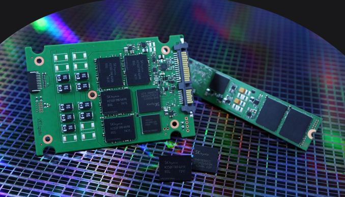
SK Hynix did not disclose when it expects to ship its enterprise drives to customers, but if its product catalogue is to be believed, the high-capacity SATA drives will be available commercially in the third quarter. Meanwhile, since we are dealing with enterprise SSDs, existing clients of SK Hynix will adopt them when they are satisfied with their real-world performance, reliability, endurance and other factors, so they may start using them ahead of Q3, or later.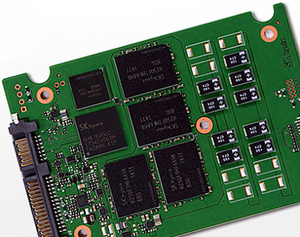
Related Reading- SK Hynix Launches 72-Layer 256 Gb 3D TLC NAND with Increased Performance
- SK Hynix Lays Out Plans for 2017: 10nm-Class DRAM, 72-Layer 3D NAND
- Toshiba Samples 64-Layer 512 Gb BiCS 3D NAND, Announces 1 TB BGA SSD
- Micron 2017 Roadmap Detailed: 64-layer 3D NAND, GDDR6 Getting Closer, & CEO Retiring
More...
-
02-08-18, 10:28 PM #7844
Anandtech: NVIDIA Announces Record Q4 2018 Results
This afternoon NVIDIA announced yet another record quarter, with revenues of $2.91 billion, which is up 34% from a year ago. Gross margin was 61.9%, and operating income was up 46% to $1.07 billion. Net income for the quarter was $1.12 billion, up 71% from a year ago, which provided diluted earnings per share of $1.78.
For their 2018 fiscal year, NVIDIA racked up $9.71 billion in revenue, which is up 41% from a year ago. Earnings per share for the year were $4.82, up 88%.NVIDIA Q4 2018 Financial Results (GAAP) Q4'2018 Q3'2018 Q4'2017 Q/Q Y/Y Revenue $2911M $2636M $2173M +10% +34% Gross Margin 61.9% 59.5% 60.0% +2.4% +1.9% Operating Income $1073M $895M $733M +20% +46% Net Income $1118M $838M $655M +33% +71% EPS $1.78 $1.33 $0.99 +34% +80%
NVIDIA has kind of hit a magic sweet spot, where they had been diversifying into growing markets, but have found themselves also swept up in the GPU fed craze of cryptocurrency, feeding their core business as well.
Gaming, which is their GeForce lineup, had revenues for the quarter of $1.74 billion, up almost $400 million from a year ago. But for the entire fiscal year, they haven’t even refreshed their lineup, although the Pascal series of GPUs have certainly been strong in terms of performance and efficiency. But you’d be lucky to find any in stock thanks to the copious number of GPUs purchased for mining coins. It’s not been ideal for gamers, but for NVIDIA’s R&D, and their investors, it’s been welcome news.
Professional Visualization was also up about 13% to $254 million. Growth here was attributed to the ultra-high-end and high-end desktop workstations, such as the Quadro GP100 launched earlier in the fiscal year.
NVIDIA’s foray into the datacenter is also paying off with substantial growth. Datacenter includes Tesla, GRID, and DGX systems, and for the quarter, NVIDIA saw revenues of $606 million, which are up 105% from a year ago.
Automotive was up a more modest 3% to $132 million, and we’ve seen NVIDIA get some big design wins with large automotive companies with their DRIVE platforms.
Automotive is powered by Tegra, and including the automotive sales, Tegra brought in $450 million this quarter, and the very popular Nintendo Switch is likely a nice chunk of that.
OEM and IP was $180 million for the quarter, which is up about 2.2%, and NVIDIA stated their licensing agreement with Intel concluded in the first quarter of fiscal year 2018.
For Q1 2019, NVIDIA is forecasting revenues of $2.9 billion, plus or minus 2%.NVIDIA Quarterly Revenue Comparison (GAAP)
($ in millions)In millions Q4'2018 Q3'2018 Q4'2017 Q/Q Y/Y Gaming $1739 $1561 $1348 +11% +29% Professional Visualization $254 $239 $225 +6% +13% Datacenter $606 $501 $296 +21% +105% Automotive $132 $144 $128 -8% +3% OEM & IP $180 $191 $176 -6% +2%
Source: NVIDIA Investor Relations
More...
-
02-09-18, 09:10 AM #7845
Anandtech: The EVGA X299 Micro Motherboard Review: A Smaller Take on X299
The EVGA X299 Micro Motherboard is mid-range microATX offering aiming to please a wide range of users but isn't marketed towards any one function in particular. It supports 2-way multi-GPU, includes a U.2 port, an M.2 slot, and has Wi-Fi connectivity via an included card. It sits as the second smallest commercial X299 motherboard, behind the X299E-ITX.
More...
-
02-12-18, 03:10 AM #7846
Anandtech: The Snapdragon 845 Performance Preview: Setting the Stage for Flagship And
In what has become an annual tradition for Qualcomm, the company has once again opened the doors of their San Diego headquarters to the press to take a preview look at the next generation of their flagship mobile platform. These events have been going on for several years now, and have become an integral part of how Qualcomm approaches the public with their wares; preview events not only let them set expectations, but to get the word out to technically-minded audiences in a vendor-neutral manner. Rather than being one part in the next flagship smartphone, preview day means that everything can be about Qualcomm and the platforms that they have created.
Late last year Qualcomm announced the Snapdragon 845 platform, the successor to 2017’s Snapdragon 835. Implementing a number of important architectural improvements over its predecessor, the Snapdragon 845 gets to follow-up on what ended up being a rather well-received platform in the Snapdragon 835, and to see if Qualcomm can maintain their momentum. Qualcomm used their December event to release a good bit of info on the 845 in advance, so we’ve already had a chance to see what Qualcomm is planning architecturally. And now with the preview event we finally get to see how all of this comes together with a look at the platform as a whole.
More...
-
02-12-18, 09:48 AM #7847
Anandtech: Marrying Vega and Zen: The AMD Ryzen 5 2400G Review
AMD's new launch of APUs hits the apex of the 2017 designs that tend the balance sheet black. After a return to high performance on x86 with the Ryzen CPU product line, and the 'we can't product enough' Vega graphics, AMD has inserted several product lines that combine the two. Today is the launch of the desktop socket edition APUs, with four Zen cores and up to 11 Vega compute units. AMD has historically been aggressive in the low-end desktop space, effectively killing the sub-$100 discrete graphics market. The new APUs now set the bar even higher. In this review we focus on the Ryzen 5 2400G, but also test the Ryzen 3 2200G.
More...
-
02-12-18, 12:21 PM #7848
Anandtech: VAIO S Laptops Updated With 8th Gen Core CPUs & TruePerformance to Prolong
VAIO has updated its popular 13-inch VAIO S laptops sold in the U.S. with Intel’s latest 8th Generation Core i5/i7 processors featuring four cores. Besides new CPUs, the systems have also added the company’s new TruePerformance technology, which is designed to maintain a higher turbo boost frequency for longer periods of time. The new VAIO S also feature a fingerprint reader and a TPM 2.0 module, emphasizing their business nature. Meanwhile the 2018 VAIO S retain their “classic” chassis along with a set of connectors, so they do not support modern headers, such as USB Type-C.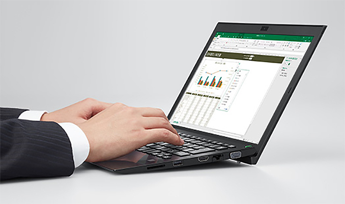
The new VAIO S laptops are based on Intel’s quad-core Core i5-8250U or Core i7-8550U processors with Intel UHD Graphics 620 accompanied by 8 – 16 GB of LPDDR3-1866 memory and a PCIe SSD featuring 256 GB, 512 GB or 1 TB capacity. One of the key features of the 2018 VAIO S notebooks is the TruePerformance technology that promises to maximize time that a CPU works at increased frequencies, giving VAIO a competitive advantage over other laptops based on the same processor.
VAIO’s TruePerformance tech is a combination of VAIO’s increased CPU power limits and a cooling system that can handle the increased heat. For reference, Intel’s Turbo Boost 2.0 technology increases the CPU frequency in increments of 100 MHz when an operating system requests a higher performance state. Typically, the amount of time that a CPU can work at its maximum Turbo Boost 2.0-defined frequency is about 20 to 30 seconds (according to VAIO), then it has to reduce its clocks because of thermals and other factors. VAIO claims that even if it increased the amount of time a processor operates at its TB 2.0-defined peak to 40 seconds, this would not bring many benefits to end users.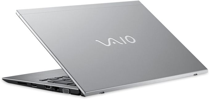
Instead, engineers from VAIO increased the base TDP limits of Intel CPUs to prolong the amount of time the chips operate at an above-nominal frequency (or frequencies), but below the TB 2.0-defined peak frequency. The company does not say whether it boosted TDP of Intel’s 8th Generation Core i5/i7 CPUs all the way to 25 W from 15 W (an increase allowed by Intel and called configurable TDP-up) which would explain and define higher frequencies. Meawhile, VAIO admits it needed to redesign its CPU VRMs as well as its cooling system to remove the extra heat. The new cooler has a thicker vent (and probably an enlarged radiator) as well as apply a new fan rotation speed control algorithm to ensure that the chips do not overheat.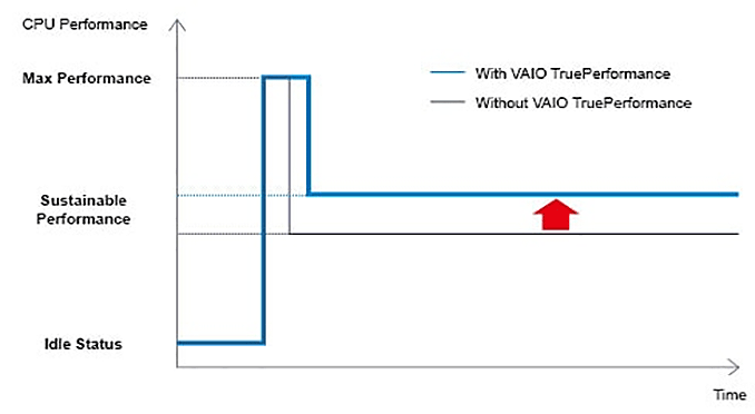
Based on graphs demonstrated by VAIO, its TruePerformance technology can increase a CPU performance in Cinebench by 11% ~ 13% when compared to the same CPU without the tech. Meanwhile, the increased TDP limit can also lift iGPU performance by 4.5% ~ 8.6%. While performance increases are not radical, they add value to VAIO’s new PCs.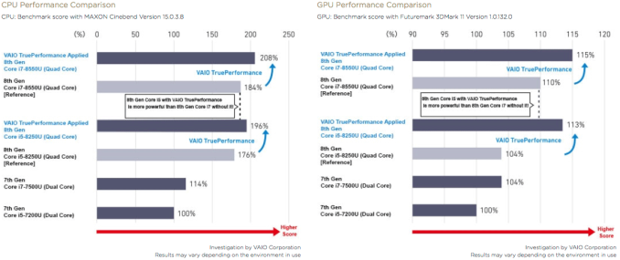
Now, back to the laptops themselves. This year’s VAIO S systems are outfitted with a 802.11ac Wi-Fi + Bluetooth 4.1 module, a GbE connector, a 0.92 MP webcam, an SD card reader, a fingerprint reader, a TPM 2.0 module and so on. Configuration of I/O ports remains unchanged from the original (non-Sony) VAIO S model launched in 2016: three USB 3.0 ports (including one always-on USB 3.0 for charging), a TRRS audio connector, an HDMI and a D-Sub output. When it comes to battery life, the new model S can work for approximately 8 hours 45 minutes on one charge, depending on the model and usage, which is in line with previous-gen VAIO S systems, but is hardly impressive when compared to other modern laptops.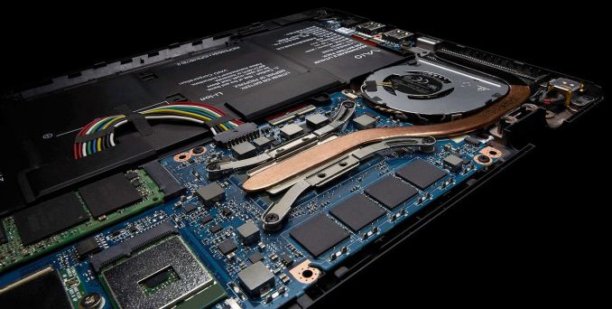
As for display and physical dimensions, the new VAIO S features a 13.3” screen with a 1920×1080 resolution, it weighs just about a kilogram (2.34 lbs) and is only 15 – 17.8 mm thick. When compared to the 2016 VAIO S, the chassis got ~1.8 mm thicker at its thinnest point and ~0.2 mm thinner at its thickest point, which is hardly a big deal for portability.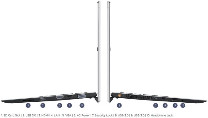
The new VAIO S will be available in the U.S. this month at MSRPs starting from $1,199. It is noteworthy that in Japan VAIO offers two business-oriented VAIO S lineups — with 11.6” and 13.3” displays (there is also a family with a 15.5” screen, but it is barely aimed at business customers). Both VAIO S11 and S13 are based on Intel’s latest quad-core Core i5/i7 8000-series processors, come with optional LTE modems and even feature spill-resistant keyboards that are never mentioned in case of the U.S. VAIO S 2018.The VAIO S 2018 at a Glance VJS132X0611S VJS132X0511S VJS132X0411S VJS132X0311S Display Size 13.3" Type IPS Resolution 1920×1080 CPU SKU Core i5-8250U Core i7-8550U Cores/Threads 4C/8T Cache 6 MB 8 MB Frequency Base 1.6 GHz 1.8 GHz cTDP-up 1.8 GHz (?) 2 GHz (?) Turbo 3.4 GHz 4 GHz TDP TDP 15 W cTDP-up 25 W (?) GPU SKU Intel HD Graphics 620 (GT2)
24 EUs, Gen 9Base 300 MHz Turbo 1.1 GHz 1.15 GHz DRAM 8 GB LPDDR3-1866 16 GB LPDDR3-1866 SSD 256 GB PCIe 512 GB PCIe 1 TB PCIe USB 3 × USB 3.0 Type-A (one w/charge) Card Reader SD card reader Wi-Fi 2×2 802.11ac Bluetooth 4.1 Ethernet GbE Display Outputs D-Sub
HDMIAudio Stereo Speakers
Microphone
TRRS audio jack for headsetsWebcam 0.92 MP webcam Fingerprint Reader Yes Battery Life 8 hours 45 minutes Dimensions Width 12.61" | 32 cm Depth 8.53" | 21.66 cm Thickness 0.59" - 0.7" | 15 - 17.8 mm Weight 2.34 lbs | 1.06 kg Colors Silver Price at Launch $1,199 $1,599 $1,899 $2,199
Related Reading:
- VAIO to Start Selling Laptops in the U.S. This Spring
- VAIO Launches Phone A: Snapdragon 617, 3 GB RAM, 5.5” FHD, Android
- VAIO to Start Selling Smartphones in Japan
More...
-
02-12-18, 12:21 PM #7849
Anandtech: AM4 Motherboard BIOS Updates Released to Support AMD Ryzen APUs
AMD’s Ryzen CPUs made a large impact on the market starting around mid-2017 when they were released. When Ryzen based CPUs hit the scene, performance was on generally on par or better than its Intel counterparts and pricing was notably better for the same thread count. This was a dramatic change from previous generations and brought competition back to the CPU market. Fast forward to today and AMD's new Ryzen-based APUs are being released – the Raven Ridge-based Ryzen 5 2400G and Ryzen 3 2200G – which merge AMD's Vega GPU architecture along with Ryzen CPU.
With this latest release of what AMD is calling their 2000-series processors, existing X370, B350, and A320 based motherboards will require a BIOS update for proper support of the new APUs. As a result, all of the major board partners have released updates for their respective lineups to include AMD's AGESA 1.1.0.1 microcode, allowing existing boards to fully support these new APUs.
In accordance with this latest round of updates, we have compiled a list from four major OEMs of all the updated BIOS versions below. Missing is Biostar who did not make any announcements. We checked the website and as of today, they have not released new BIOSes for their AM4 boards which include the AGESA 1.1.0.1 update supporting these APUs.
MSI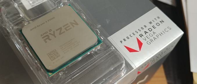
MSI distributed a press release a couple days ago on its website. These can be found at the motherboard's site and the support section.
AsusMSI X370 Motherboards Name PCB Version BIOS Version X370 XPower Gaming Titanium 1.1 E731AMS.1C0 X370 Gaming M7 ACK 1.1 E7A35AMS.150 X370 Gaming Pro Carbon AC 1.1 E7A32AMS.280 X370 Gaming Pro Carbon 1.1 E732AMS.1C0 X370 Krait Gaming 1.0 / 1.1 E7A33AMS.190 X370 Gaming Pro 2.0 / 2.1 E733AMS.480 X370 SLI Plus 2.0 / 2.1 E7A33AMS.390 X370 Gaming Plus 3.0 E7A33AMS.580 B350 B350 Gaming Pro Carbon 1.1 E7B00AMS.190 B350 Krait Gaming 1.0 E7B08AMS.180 B350 Tomahawk Plus 1.2 E7B36AMS.180 B350 Tomahawk 1.0 E7A34AMS.1C0 B350 Tomahawk Arctic 3.0 E7A34AMS.HA0 B350 Gaming Plus 4.0 E7A34AMS.M70 B350M Mortar 1.1 E7A37AMS.1B0 B350M Mortar Arctic 2.1 E7A7AMS.AA0 B350M Bazooka 1.0 E7A38AMS.1A0 B350M Gaming Pro 1.0 E7A39AMS.2C0 B350 PC Mate 2.0 E7A34AMS.AA0 B350M Pro-VD Plus 1.1 E7B38AMS.250 B350M Pro-VDH 2.0 E7A38AMS.A90 B350I-S01 1.1 E7A40AMS.230 B350I Pro AC 1.1 E7A40AMS.110B350M Pro-VH Plus 1.0 E7B07AMS.250 A320 A320M Gaming Pro 1.0 E7A39AMS.190 A320M Bazooka 1.0 E7A38AMS.280 A320M Grenade 3.0 E7A39AMS.A80 A320M Pro-VD/S 1.0 E7A36AMS.270 A320M Pro-VH Plus 1.0 E7B07AMS.360 A320M Pro-VHL 1.0 E7B07AMS.160 A320M Pro-VD Plus 1.0 E7B38AMS.310 A320M Pro-VD Plus 1.1 E7B38MAS.150
Asus also sent out an official announcement on their new BIOSes. The Asus website lists them as well as instructions on how to update. The X370 Crosshair motherboards are able to flash via BIOS Flashback or EX Flash 3 while the rest of the of the boards will use the more traditional EX Flash 3.
ASRockAsus X370 Motherboards Name BIOS Version ROG Crosshair VI Extreme 3502 ROG Crosshair VI Hero (Wi-Fi AC) 3502 ROG Crosshair VI Hero 3502 ROG Strix X370-F Gaming 3803 ROG Strix X370-I Gaming 3803 Prime X370-Pro 3803 Prime X370-A 3803 B350 ROG Strix B350-F Gaming 3803 ROG Strix B350-I Gaming 3803 TUF B350M-Plus Gaming 3803 Prime B350-Plus 3803 Prime B350M-A 3803 Prime B350M-E 3803 Prime B350M-K 3803 B350M-Dragon 3803 A320 Prime A320M-C R2.0 3803 Prime A320M-A 3803 Prime A320M-E 3803 Prime A320M-K 3803 EX-A320M-Gaming 3803
ASRock also made an announcement, however, it was only on their Japanese website or via email to the press. Since that was published, additional BIOSes have already been released and are listed below.
GIGABYTEASRock X370 Motherboards Name BIOS Version X370 Taichi 4.40 X370 Killer SLI/AC 4.50 X370 Killer SLI 4.50 Fatal1ty X370 Professional Gaming 4.40 Fatal1ty X370 Gaming K4 4.50 Fatal1ty X370 Gaming X 4.50 Fatal1ty X270 Gaming-ITX/AC 4.40 B350 AB350 Pro4 4.50 AB350M Pro4 4.50 AB350M 4.40 AB350M-HDV 4.40 Fatal1ty AB350 Gaming-ITX/AC 4.40 Fatal1ty AB350 Gaming K4 4.60 A320 A320M Pro4 4.50 A320M 4.40 A320M-DGS 4.40 A320M-HDV 4.40
GIGABYTE did not have an official announcement but are listed on the website for all AM4 motherboards.
Related Reading:GIGABYTE X370 Motherboards Name BIOS Version GA-AX370M-Gaming 3 F20 GA-AX370M-DS3H F20 GA-AX370-Gaming K7 F20 GA-AX370-Gaming K5 F20 GA-AX370-Gaming K3 F20 GA-AX370-Gaming 5 F20 GA-AX370-Gaming 3 F20 GA-AX370-Gaming F20 B350 GA-AB350M-Gaming 3 F20 GA-AB350N-Gaming WiFi T20h GA-AB350M-DS3H F20 GA-AB350M-D3V F20 GA-AB350M-HD3 F20 GA-AB350M-DS2 F20 GA-AB350-D3H F20 GA-AB350-Gaming 3 F20 GA-AB350-Gaming F20 A320 GA-A320M-S2H F20 GA-A320MA-M.2 F20 GA-A320M-D2P F20 GA-A320M-DS2 F20 GA-A320M-HD2 F20 GA-A320-DS3 F20 - Marrying Vega and Zen: The AMD Ryzen 5 2400G Review
- AMD Tech Day at CES: 2018 Roadmap Revealed, with Ryzen APUs, Zen+ on 12nm, Vega on 7nm
- Ryzen Mobile is Launched: AMD APUs for Laptops, with Vega and Updated Zen
- The AMD Ryzen 3 1300X and Ryzen 3 1200 CPU Review: Zen on a Budget
- The AMD Zen and Ryzen 7 Review: A Depp Dive on 1800X, 1700X, and 1700
More...
-
02-12-18, 02:01 PM #7850
Anandtech: AMD Readies Ryzen 3 2200GE & Ryzen 5 2400GE APUs with Reduced TDP
AMD is preparing to release low-power versions of its Ryzen APUs with built-in Radeon Vega graphics. The new Ryzen 3 2200GE and Ryzen 5 2400GE chips will have a 35 W TDP and will operate at lower frequencies when compared to the Ryzen 3 2200G and the Ryzen 5 2400G that hit the market this week. ASUS has already added support for the new energy-efficient APUs to BIOS of one of its AM4 motherboards, so the actual launch is imminent.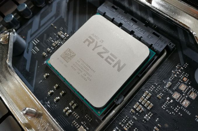
AMD’s Ryzen 3 2200G with Radeon Vega 8 graphics as well as Ryzen 5 2400G with Radeon RX Vega 11 graphics have configurable TDP of 45 - 65 W and enable AMD to compete for mainstream desktops. This market is rather big and it is important to address it with competitive offerings, but sales of traditional desktops are stagnating at best. Meanwhile, demand for small form-factor desktops is growing, so AMD has to offer processors with reduced power consumption to address them. The company already has multiple energy-efficient Excavator-based APU for the AM4 platform in its arsenal and in the coming weeks or months it will release Zen-based APUs for SFF desktops.
Initially, AMD plans to offer two energy-efficient Zen-based APUs: the Ryzen 3 2200GE and the Ryzen 5 2400GE. Both APUs feature four Zen cores as well as Radeon Vega graphics, but their exact specs and configs are yet to be disclosed. According to ASUS, the Ryzen 5 2400GE will feature four cores with SMT operating at 3.2 GHz (down from 3.6 GHz of the Ryzen 5 2400G) as well as a 35 W TDP. Meanwhile, the Ryzen 3 2200GE appears to feature four cores without SMT working at 3.2 GHz (down from 3.5 GHz of the 2200G) along with a 35 W TDP*. It remains to be seen whether AMD’s Ryzen 3 2200GE and Ryzen 5 2400GE sustain iGPU configurations of their higher-power brethren (obviously, at reduced clocks) as well as DDR4-2933 support, but at this point base CPU frequencies is all we know about these products.
The 35W Ryzen APUs will enable AMD to compete for OEM SFF and ultra-slim Mini-ITX DIY builds (previous-gen Bristol Ridge chips were hardly attractive for enthusiasts), which will help the company to further increase its market share.AMD Ryzen 2000-Series APUs Ryzen 5
2400G
with Vega 11Ryzen 5
2400GE
with Vega 11Ryzen 3
2200G
with Vega 8Ryzen 3
2200G
with Vega 8CPU Cores/Threads 4 / 8 4 / 4 Base CPU Frequency 3.6 GHz 3.2 GHz 3.5 GHz 3.2 GHz (?) Turbo CPU Frequency 3.9 GHz ? 3.7 GHz ? TDP @ Base Frequency 65 W 35 W 65 W 35 W Configurable TDP 46-65 W 35 W 46-65 W 35 W L2 Cache 512 KB/core L3 Cache 4 MB Graphics Vega 11 Vega 11 (?) Vega 8 Vega 8 (?) Compute Units 11 CUs 11 CUs (?) 8 CUs 8 CU (?) Streaming Processors 704 SPs 704 SPs (?) 512 SPs 512 (?) Base GPU Frequency 1250 MHz ? 1100 MHz ? DRAM Support DDR4-2933
Dual ChannelDDR4
Dual ChannelDDR4-2933
Dual ChannelDDR4
Dual ChannelOPN PIB YD2400C4FBBOX ? YD2200C5FBBOX ? OPN Tray YD2400C5M4MFB ? YD2200C4M4MFB ? Price $169 ? $99 ? Bundled Cooler AMD Wraith Stealth ? AMD Wraith Stealth ?
AMD did not comment on the news story because the Ryzen 3 2200GE and the Ryzen 5 2400GE have not been announced, so we cannot fill the gaps when it comes to specs and prices of the new APUs.
*Specifications of the Ryzen 3 2200GE are a bit less clear from the ASUS listings because the company attributes partially correct specs of the Ryzen 3 2200G (the L3 cache size the company cites is incorrect) to the 2200GE (see the image below). Now, if the company attributes specs of the 2200GE to the 2200G, then we have basic specifications of the former, but if there is a mistake somewhere, we do not and the 3.2 GHz base frequency figure is inaccurate.
Related Reading: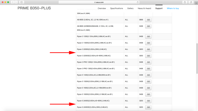
- Marrying Vega and Zen: The AMD Ryzen 5 2400G Review
- AMD Tech Day at CES: 2018 Roadmap Revealed, with Ryzen APUs, Zen+ on 12nm, Vega on 7nm
More...


 Quote
QuoteThread Information
Users Browsing this Thread
There are currently 33 users browsing this thread. (0 members and 33 guests)


Bookmarks