

Results 10,021 to 10,030 of 12091
Thread: Anandtech News
-
11-05-19, 12:31 PM #10021
Anandtech: Dells Introduces UltraSharp 27-Inch 4K Monitor (UP2720Q) With Integrated
Just in time for this week's Adobe MAX conference, Dell has introduced an updated version of its popular 27-inch 4K UltraSharp professional display. The latest iteration of Dell's pro monitor, the UltraSharp 27 4K PremierColor Monitor (UP2720Q) is shaking things up by taking the already factory-calibrated monitor family and integrating a colorimeter for even further calibration options, as well as Thunderbolt 3 support. At the same time, however, Dell is also dropping HDR support, making this (once again) a purely SDR display.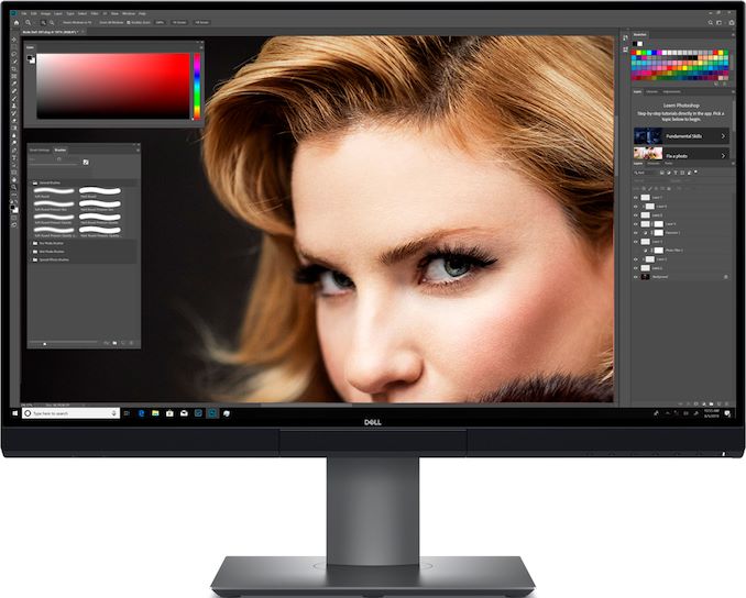
Like its predecessors, the UltraSharp 27 4K PremierColor Monitor UP2720Q is particularly aimed at photographers, designers, and other people with color-critical workloads. The LCD comes factory calibrated to a Delta
-
11-05-19, 02:19 PM #10022
Anandtech: Seagate: 18 TB HDD Due in First Half 2020, 20 TB Drive to Ship in Late 202
Seagate last week clarified its high-capacity HDD roadmap during its earnings call with analysts and investors. The company is on track to ship its first commercial HAMR-based hard drives next year, but only in the back half of the year. Before that, Seagate intends to ship its 18 TB HDDs.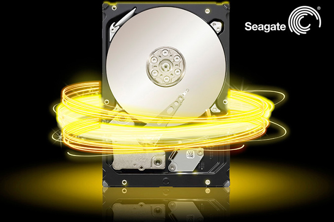
It is expected that Seagate’s 18 TB hard drive will be based on the same nine-platter platform that is already used for the company’s Exos 16 TB HDD, which means that it will be relatively easy for the company to kick off mass production of 18 TB hard drives. Overall, Seagate’s HDD roadmap published in September indicates that the company’s 18 TB drive will use conventional magnetic recording (CMR) technology. In addition to this product, Seagate’s plans also include a 20 TB HDD based on shingled magnetic recording (SMR) technology that is due in 2020.
Seagate says that its Exos 16 TB hard drives are very popular among its clients and even expects to ship more than a million of such drives in its ongoing quarter, which ends in December. The launch of its 18 TB HDD will maintain Seagate’s capacity leadership in the first half of next year before Western Digital starts volume shipments of its HAMR+CMR-based 18 TB and HAMR+SMR-based 20 TB hard drives.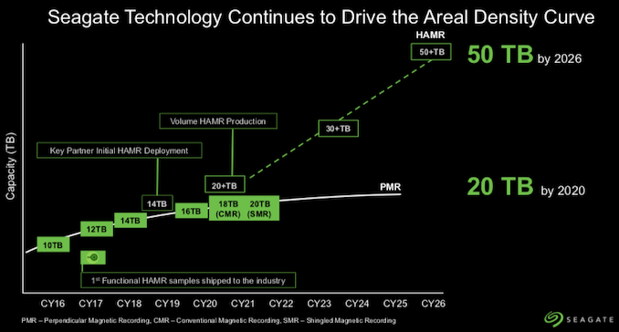
Seagate itself will be ready with its HAMR-based 20 TB drive late in 2020. Right now, select Seagate customers are qualifying HAMR-based 16 TB HDDs, so they will likely be ready to deploy 20 TB HAMR drives as soon as they are available. It is noteworthy that Seagate is readying HAMR HDDs with both one and two actuators, as to offer the right performance and capacity for different customers. This would follow Seagate's current dual-actuator MACH.2 drives, which the company started shipping for revenue last quarter.
Dave Mosley, CEO of Seagate, said the following:
“We are preparing to ship 18 TB drives in the first half of calendar year 2020 to maintain our industry capacity leadership. We are also driving areal density leadership with our revolutionary HAMR technology, which enables Seagate to achieve at least 20% areal density CAGR over the next decade. We remain on track to ship 20 TB HAMR drives in late calendar year 2020.Related Reading:
As drive densities increase, multi-actuator technology is required to maintain fast access to data and scale drive capacity without compromising performance. We generated revenue from our MACH.2 dual actuator solutions for the first time in the September quarter. We are working with multiple customers to qualify these drives, including a leading US hyperscale customer, who is qualifying the technology to meet their rigorous service level agreements without having to employ costly hardware upgrades. We expect to see demand for dual actuator technology to increase as customers transition to drive capacities above 20 TB.”
- State of the Union: Seagate's HAMR Hard Drives, Dual-Actuator Mach2, and 24 TB HDDs on Track
- Seagate Ships 16 TB CMR Hard Drives, Preps 18 TB SMR HDDs
- Seagate Starts to Test 16 TB HAMR Hard Drives
Source: Seagate
More...
-
11-05-19, 06:13 PM #10023
Anandtech: GlobalFoundries and SiFive to Design HBM2E Implementation on 12LP/12LP+
GlobalFoundries and SiFive announced on Tuesday that they will be co-developing an implementation of HBM2E memory for GloFo's 12LP and 12LP+ FinFET process technologies. The IP package will enable SoC designers to quickly integrate HBM2E support into designs for chips that need significant amounts of bandwidth.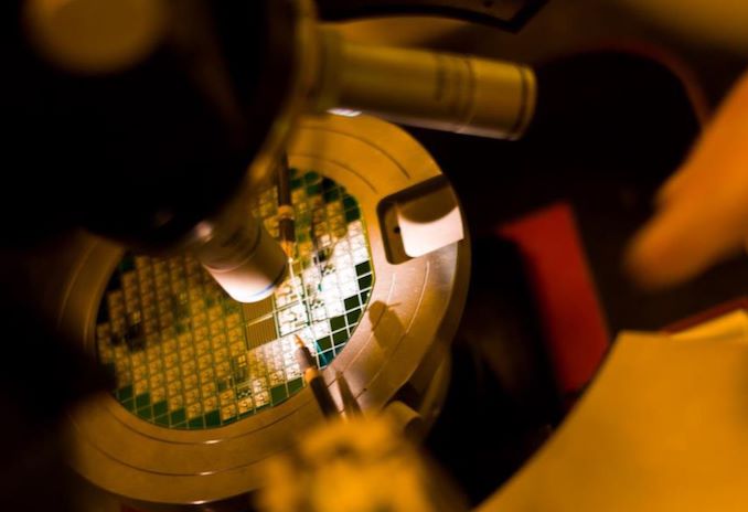
The HBM2E implementation by GlobalFoundries and SiFive includes the 2.5D packaging (interposer) designed by GF, with the HBM2E interface developed by SiFive. In addition to HBM2E technology, licensees of SiFive also gain access to the company’s RISC-V portfolio and DesignShare IP ecosystem for GlobalFoundries’ 12LP/12LP+, which will enable SoC developers to build RISC-V-based devices GloFo's advanced fab technology.
GlobalFoundries and SiFive suggest that the 12LP+ manufacturing process and the HBM2E implementation will be primarily used for artificial intelligence training and inference applications for edge computing, with vendors looking to optimize for TOPS-per-milliwatt performance.
For GlobalFoundries, it is important to land customers who need specialized process technologies and may not be ready for leading-edge processes from TSMC and Samsung Foundry for cost or other reasons. As for SiFive's involvement, this is a bit trickier – RISC-V itself isn't likely to be used for the core logic in deep learning accelerators, but it is a solid architecture to use for the embedded CPU cores needed to control the dataflows within an accelerator.
SiFive’s HBM2E interface and custom IP for GlobalFoundries’ 12LP and 12LP+ technology are being developed at GF’s Fab 8 in Malta, New York. The two companies expect that they'll be able to wrap up their work in the first half of 2020, at which point the IP will become available for licensing.
Related Reading:
- GlobalFoundries Unveils 12LP+ Technology: Massive Performance & Power Improvements
- SiFive Announces First RISC-V OoO CPU Core: The U8-Series Processor IP
- Samsung Develops 12-Layer 3D TSV DRAM: Up to 24 GB HBM2
- Samsung HBM2E ‘Flashbolt’ Memory for GPUs: 16 GB Per Stack, 3.2 Gbps
- SK Hynix Announces 3.6 Gbps HBM2E Memory For 2020: 1.8 TB/sec For Next-Gen Accelerators
- SiFive Acquires USB 2.0 and 3.x IP Portfolio to Strengthen RISC-V SoCs
Source: GlobalFoundries
More...
-
11-05-19, 09:28 PM #10024
Anandtech: Intels EMIB Now Between Two High TDP Die: The New Stratix 10 GX 10M FPGA
The best thing about manufacturing Field Programmable Gate Arrays (FPGAs) is that you can make the silicon very big. The nature of the repeatable unit design can absorb issues with a process technology, and as a result we often see FPGAs be the largest silicon dies that enter the market for a given manufacturing process. When you get to the limit of how big you can make a piece of silicon (known as the reticle limit), the only way to get bigger is to connect that silicon together. Today Intel is announcing its latest ‘large’ FPGA, and it comes with a pretty big milestone with its connectivity technology.
More...
-
11-06-19, 12:27 PM #10025
Anandtech: MLPerf Releases Official Results For First Machine Learning Inference Benc
Since launching their organization early last year, the MLPerf group has been slowly and steadily building up the scope and the scale of their machine learning benchmarks. Intending to do for ML performance what SPEC has done for CPU and general system performance, the group has brought on board essentially all of the big names in the industry, ranging from Intel and NVIDIA to Google and Baidu. As a result, while the MLPerf benchmarks are still in their early days – technically, they’re not even complete yet – the group’s efforts have attracted a lot of interest, which vendors are quickly turning into momentum.
Back in June the group launched its second – and arguably more interesting – benchmark set, MLPerf Inference v0.5. As laid out in the name, this is the MLPerf group’s machine learning inference benchmark, designed to measure how well and how quickly various accelerators and systems execute trained neural networks. Designed to be as much a competition as it is a common and agreed upon means to test inference performance, MLPerf Inference is intended to eventually become the industry’s gold standard benchmark for measuring inference performance across the spectrum, from low-power NPUs in SoCs to dedicated, high-performance inference accelerators in datacenters. And now, a bit over 4 months after the benchmark was first released, the MLPerf group is releasing the first official results for the inference benchmark.
More...
-
11-06-19, 12:27 PM #10026
Anandtech: NVIDIA Gives Jetson AGX Xavier a Trim, Announces Nano-Sized Jetson Xavier
Since it was launched earlier this decade, NVIDIA’s Jetson lineup of embedded system kits remains one of the odder success stories for the company. While NVIDIA’s overall Tegra SoC plans have gone in a very different direction than first planned, they’ve seen a lot of success with their system-level Jetson kits, as customers snatch them up both as dev kits and for use in commercial systems. Now in their third generation of Jetson systems, this afternoon NVIDIA is outlining their plans to diversify the family a bit more, announcing a physically smaller and cheaper version of their flagship Jetson Xavier kit, in the form of the Jetson Xavier NX.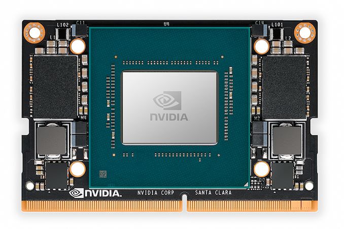
Based on the same Xavier SoC that’s used in the titular Jetson AGX Xavier, the Jetson Xavier NX is designed to fill what NVIDIA sees as a need for both a cheaper Xavier option, as well as one smaller than the current 100mm x 87mm board. In fact the new Nano-sized board is quite literally that: the size of the existing Jetson (TX1) Nano, which was introduced earlier this year. Keeping the same form factor and pin compatibility, the Jetson Xavier NX sports the same 45mm x 70mm dimensions, making it a bit smaller than a credit card.
Compared to the full-sized Jetson AGX Xavier, NVIDIA is aiming the Jetson Xavier NX at customers who need to do edge inference in space-constrained use cases where the big Xavier won’t do. Since it’s based on the same Xavier SoC, the Jetson Xavier NX uses the same Volta GPU, and critically, the same NVDLA accelerator cores as the original. As a result, for inference tasks the Jetson Xavier NX should be significantly faster than the Jetson Nano and various Jetson TX2 products – curently NVIDIA's most widely used embedded Jetson – none of which have hardware comparable to NVIDIA’s dedicated deep learning accelerator cores.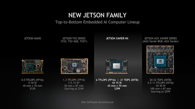
Not that Jetson Xavier NX is a wholesale replacement for Jetson AGX Xavier, however. The smaller Xavier board is taking a shave both in performance and in I/O for a mix of product segmentation, power consumption, and pin compatibility reasons. Notably, the Xavier SoC uses in the NX loses out on 2 CPU cores, 2 GPU SMs, and perhaps most important to heavy inference users, half of the chip’s memory bandwidth. As a result the Jetson Xavier NX should still be significantly ahead of Jetson TX1/TX2, but it will definitely trail the full-fledged Jetson AGX Xavier.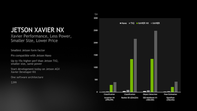
All told, for inference applications NVIDIA is touting 21 TOPS of performance at the card’s full power profile of 15 Watts. Alternatively, at 10 Watts – which happens to be the max power state for Jetson Nano – this drops down to 14 TOPS as clockspeeds are reduced and two more CPU cores are shut off.NVIDIA Jetson Family Specifications Xavier NX
(15W)Xavier NX
(10W)AGX Xavier Jetson Nano CPU 4x/6x Carmel
@ 1.4GHz
or
2x Carmel
@ 1.9GHz4x/ Carmel
@ 1.2GHz
or
2x Carmel
@ 1.5GHz8x Carmel
@ 2.26GHz4x Cortex-A57
@ 1.43GHzGPU Volta, 384 Cores
@ 1100MHzVolta, 384 Cores @ 800MHz Volta, 512 Cores
@ 1377MHzMaxwell, 128 Cores
@ 920MHzAccelerators 2x NVDLA 2x NVDLA N/A Memory 8GB LPDDR4X, 128-bit bus
(51.2 GB/sec)16GB LPDDR4X, 256-bit bus
(137 GB/sec)4GB LPDDR4, 64-bit bus
(25.6 GB/sec)Storage 8GB eMMC 32GB eMMC 16GB eMMC AI Perf. 21 TOPS 14 TOPS 32 TOPS N/A Dimensions 45mm x 70mm 100mm x 87mm 45mm x 70mm TDP 7.5W 15W 30W 10W Price $399 $999 $129
Otherwise, the Jetson Xavier NX is designed to slot right in with the rest of the Jetson family, as well as NVIDIA’s hardware and software ecosystem. The embedded system board is being positioned purely for use in high-volume production systems, and accordingly, NVIDIA won’t be putting together a developer kit version of the NX. Since the current Jetson AGX Xavier will be sticking around, it will fill that role, and NVIDIA is offering software patches for developers who need to specifically test against Jetson Xavier NX performance levels.
The Jetson Xavier NX will be shipping from NVIDIA in March of 2020, with NVIDIA pricing the board at $399.
More...
-
11-06-19, 04:00 PM #10027
Anandtech: New 17cm GeForce GTX 1660 Super Graphics Cards
Last week NVIDIA introduced its latest GeForce GTX 1660 Super performance mainstream GPU. There are plenty of designs to chose from, and both ASUS and GIGABYTE are now set to offer small form factor designs.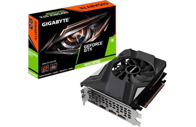
ASUS has two new GeForce GTX 1660 Super boards that are 17.4 centimeters (6.9 inches) long. The ASUS Phoenix PH-GTX1660S-6G and Phoenix PH-GTX1660S-O6G cards are based on NVIDIA’s TU116 GPU with 1408 CUDA cores, carry 6 GB of GDDR6 memory, share the same PCB design with one 8-pin auxiliary PCIe power connector, feature three display outputs (DVI-D, DP 1.4, HDMI 2.0b), and use the same dual-slot cooling system with one dual ball bearing fan. The only difference between the two are their clocks and even they are pretty close: up to 1815 MHz vs 1830 MHz in OC mode.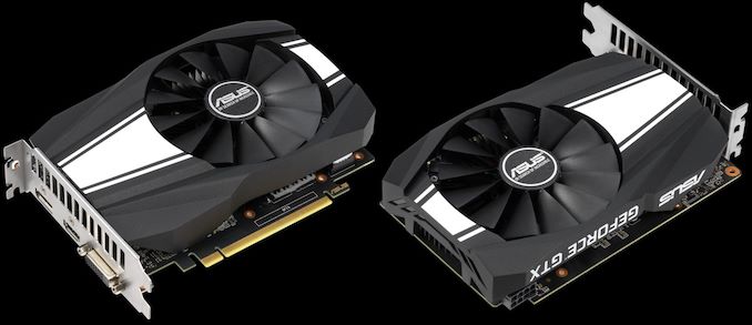
GIGABYTE has a more 'canonical' GeForce GTX 1660 Super Mini ITX OC 6G (GV-N166SIXOC-6GD) board that is exactly 17 centimeters long. The card has NVIDIA’s TU116 GPU clocked at up to 1800 MHz, 6 GB of 14 Gpbs GDDR6 RAM, uses a dual-slot single-fan cooler with a heat pipe that can stop the fan in idle mode, has an 8-pin PCIe power connector, and offers four display outputs (DP 1.4, HDMI 2.0b).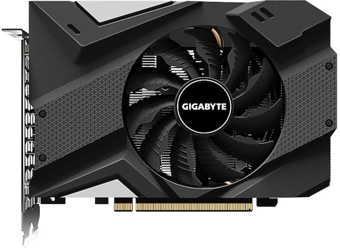
All three graphics cards are listed at ASUS’ and GIGABYTE’s websites, so expect them to be available shortly. Pricing wise, they should not be much more expensive than NVIDIA’s $229 MSRP for the GeForce GTX 1660 Super.NVIDIA GeForce GTX 1660 Super Graphics Cards for Mini-ITX NVIDIA
ReferenceASUS
Phoenix
PH-GTX1660S-6GASUS
Phoenix
PH-GTX1660S-O6GGIGABYTE
GV-N166SIXOC-6GDCUDA Cores 1408 ROPs 48 Core Clock 1530 MHz 1530 MHz (?) Boost Clock 1785 MHz 1815 MHz 1830 MHz 1800 MHz Memory Clock 14 Gbps GDDR6 Memory Bus Width 192-bit VRAM 6 GB Single Precision Perf. 5 TFLOPS ~5 TFLOPS Display Outputs 1×DVI-D
1×DP 1.4
1×HDMI 2.0b1×DVI-D
1×DP 1.4
1×HDMI 2.0b3×DP 1.4
1×HDMI 2.0bTGP 125W ? ? ? GPU TU116
(284 mm2)Transistor Count 6.6B Architecture Turing Manufacturing Process TSMC 12nm "FFN" Launch Date 10/29/2019 Q4 2019 Launch Price $229 ? ? ?
Related Reading- The NVIDIA GeForce GTX 1660 Super Review, Feat. EVGA SC Ultra: Recalibrating The Mainstream Market
- NVIDIA Announces GeForce GTX 1650 Super: Launching November 22nd
- MSI & ZOTAC with New Double-Slot Low-Profile GeForce GTX 1650 GPUs
Sources: ASUS (1, 2), GIGABYTE
More...
-
11-06-19, 04:00 PM #10028
Anandtech: Western Digital Ultrastar DC SS540 SAS SSDs: Up to 15.36 TB, Up to 3 DWPD
Western Digital has introduced its new series of SSDs designed for mission critical applications, including OLTP, OLAP, hyper converged infrastructure (HCI), as well as software-defined storage (SDS) workloads. The Ultrastar DC SS540 drives are aimed at mixed and write intensive workloads and can be configured accordingly. Since the SSDs use an SAS 12 Gbps interface, they are drop in compatible with existing machines.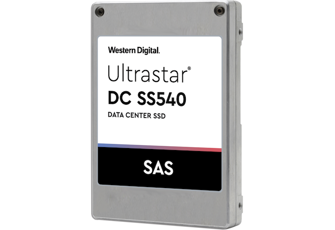
The Western Digital Ultrastar DC SS540 is based on the company's sixth-generation dual-port SAS 12 Gbps platform co-developed with Intel as well as 96-layer 3D TLC NAND memory (presumably, also from Intel) and comes in a 2.5-inch/15 mm form-factor. The new SSDs are drop-in compatible with existing servers that support 9, 11, and 14 W per drive power options (SKUs with higher power consumption offer higher random read/write speeds).
As is traditional for SAS SSDs from Western Digital and Intel, the Ultrastar DC SS540 supports extended error correction code (ECC with a 1x10^-17 bit error rate) to ensure high performance and data integrity, exclusive-OR (XOR) parity in case a whole NAND die fails, and parity-checked internal data paths. In addition, the Ultrastar SS540 complies with the T10 Data Integrity Field (DIF) standard, which requires all interconnect buses to have parity protection (on the system level), as well as a special power loss data management feature that does not use supercapacitors. As usual, Western Digital's Ultrastar SS540 will be available in different SKUs with capabilities like instant secure erase and/or TCG+FIPS encryption to conform with various security requirements.
The manufacturer plans to offer the Ultrastar DC SS540 rated for 1 or 3 drive writes per day (DWPD) to target different workloads. The former will offer capacities between 960 GB and 15.36 TB, whereas the latter will feature capacities from 800 GB to 6.4 TB. The new lineup does not include drives rated for 10 DWPD and less than 1 DWPD, so those who need higher or lower endurance (as they run extremely read intensive or extremely write intensive workloads) will have to use previous-generation offerings from Western Digital. When it comes to warranty and MTBF, the drives are rated for a 0.35% annual failure rate (AFR), 2.5 million hours MTBF and are covered with a five-year limited warranty (or the max PB written, whichever occurs first).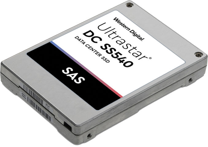
As far as sustained performance is concerned, the Ultrastar DC SS540 is rated for up to 2130 MB/s sequential read/write speed, up to 470K IOPS random write IOPS, and up to 240K random write IOPS, depending on exact model, which is generally in line with performance of the Ultrastar DC SS530 SSDs launched last year. Traditionally, higher capacity SSDs are slightly slower when it comes to writes and mixed workloads, but those who need maximum performance can always use more drives to hit desired speeds.
Western Digital’s Ultrastar DC SS540 SSDs are currently sampling and qualified by select clients of the company. The manufacturer plans to start commercial shipments of the drives in the Q1 2020.
Related Reading:HGST Ultrastar SS540 Series Specifications 3 DWPD 1 DWPD Capacities 6.4 TB
3.2 GB
1.6 TB
800 GB15.36 TB
7.68 TB
3.84 TB
1.92 TB
960 GBForm Factor 2.5"/15mm Interface SAS 6/12 Gb/s, dual port for 12 Gb/s Controller Proprietary NAND 96-layer
3D TLC NANDSequential Read 2116 ~ 2130 MB/s 1985 ~ 2130 MB/s Sequential Write 1008 MB/s ~ 2109 MB/s 1985 MB/s ~ 2130 MB/s Random Read (4 KB) IOPS 237K ~ 470K IOPS 237K ~ 470K IOPS Random Write (4 KB) IOPS 128K ~ 240K IOPS 79K ~ 110K Mixed Random R/W (70:30 R:W, 4KB)
Max IOPS182K ~ 300K IOPS 143K ~ 200K IOPS Read/Write Latency (average) 140/60 ms ~ 150/80 ms 140/90 ms ~ 150/300 ms Power Idle 3.7 W (15 TB) Operating 9 W, 11 W, 14 W (configurable) Endurance DWPD 3 1 Max. PB 6.4 TB: 36,150 TB
3.2 TB: 17,150 TB
1.6 TB: 9,410 TB
800 GB: 4.700 TB15.36 TB: 30,110 TB
7.68 TB: 15,050 TB
3.84 TB: 7,000 TB
1.92 TB: 3,760 TB
960 GB: 1,880 TBEncryption AES-256 (?)
TCG + FIPSPower Loss Protection Yes MTBF 2.5 million hours Warranty Five years or max PB written (whichever occurs first) Models WUSTR6464ABSS20x
WUSTR6432BSS20x
WUSTR6416BSS20x
WUSTR6480BSS20xWUSTVA1A1BSS20x
WUSTVA176BSS20x
WUSTVA138BSS20x
WUSTVA119BSS20x
WUSTVA196BSS20xLegend for Model Numbers Example: WUSTR6464ASS201=6.4TB, SAS 12Gb/s, TCG
W = Western Digital
U = Ultrastar
S = Standard
TR = NAND type/endurance
(TM=TLC/mainstream endurance,
TR=TLC/read-intensive) 64 = Full capacity (6.4TB) 64 = Capacity of this model
15 = 15.2TB 76 = 7.6TB 38 = 3.84TB 32 = 3.2TB 19 = 1.92TB 16 = 1.6TB 96 = 960GB 80 = 800GB 48 = 480GB 40 = 400GB
A = Generation code
S = Small form factor (2.5” SFF) S2 = Interface, SAS 12Gb/s
1 = Encryption setting
0 = Instant Secure Erase
1 = TCG Enterprise encryption
4 = No encryption/Secure Erase 5 = TCG+FIPS
- HGST Launches Ultrastar DC SS530 SSDs: 3D TLC NAND, 15.36 TB, SAS 12 Gbps
- Western Digital Reveals Ultrastar DC SN340 SSDs for Read Intensive Workloads
- Western Digital Launches HGST Ultrastar SS300 SSDs: 3D NAND for Data Centers
- HGST Ultrastar SS200 SSD: Up to 7.68 TB, 1.8 GB/s, Dual-Port SAS 12 Gbps
- HGST Ultrastar SN200 Accelerator: 7.68 TB Capacity, 6.1 GB/s Read Speed, 1.2M IOPS
Source: Western Digital
More...
-
11-07-19, 10:44 AM #10029
Anandtech: Xiaomis Mi Note 10 Family: Worlds First Smartphones with 108 MP Penta Ca
A couple of months back, Samsung announced a new ultra high resolution 108 MegaPixel sensor for smartphone cameras. At the time we didn't know where this sensor would first show up, but now we have our answer: Xiaomi. This week the company is introducing the industry’s first smartphones with a five-module (penta) camera setup, including the 108 MP sensor from Samsung. Dubbed the Mi Note 10 and Mi Note 10 Pro (and in China, the Mi CC9 Pro/Mi CC9 Pro Premium Edition), these new phones are aimed specifically at photographers, with Xiaomi taking an upper-mid-range platform and giving it one of the most extensive camera arrays on the market.
Without any doubts, the key feature of Xiaomi’s Mi Note 10 and Mi Note 10 Pro devices (and their Chinese equivalents) is their five-module rear camera featuring Samsung’s ICOCELL bright HMX 108 MP wide-angle 1/1.33-inch sensor with a 4-axis OIS, 4-in-1 pixel binning, and a 7-piece lens assembly (an 8-piece in case of the Pro model). In addition to the gargantuan 108 MP sensor, the camera array also has a 20 MP 117º ultra-wide-angle module, a 12 MP telephone module, a 5 MP telephoto module for 10x hybrid and 50x digital zoom, and a 2 MP macro camera. The whole camera setup is equipped with a quad-LED dual-tone flash. And along with the main camera, the smartphones come with a 32 MP 'waterdrop' selfie camera.
To view high-quality photos, the flagship smartphone camera is paired with a 6.47-inch SAMOLED display featuring a 2340×1080 resolution, a 19.5:9 aspect ratio, 600 nits peak brightness, the DCI-P3 color gamut, and HDR10 support.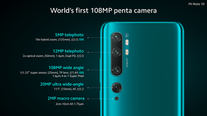
Meanwhile, at the heart of the Xiaomi’s Mi Note 10 and Mi Note 10 Pro smartphones is Qualcomm’s Snapdragon 730G SoC, which is one of Qualcomm's upper-mid-range SoCs and features two Kryo 470 Gold cores, six Kryo 470 Silver cores, and Adreno 618 graphics. That SoC is accompanied by 6 GB of RAM and 128 GB of storage in case of the regular model, as well as 8 GB of RAM and 256 GB of storage in case of the Pro model. The handsets are powered by a non-removable Li-Po 5260 mAh battery.
Rounding out the package, the new phones feature 4G/LTE, Wi-Fi 5, Bluetooth 5.0, a USB 2.0 Type-C connector, an under-display fingerprint reader, as well as all the other essential features that we come to expect in late 2019. However as these aren't full flagship-level phones, you won't find much in the way of advanced features: the phones aren't listed as dust and water resistant, there's no wireless charging, and they do not have a microSD card slot (which is a bit odd given the target audience).
Xiaomi's Mi Note 10 smartphone will be available in Midnight Black, Aurora Green, and Glacier White in Europe starting mid-November for €549. The Mi Note 10 Pro model will be priced at €649.The Xiaomi Mi Note 10 Family Mi Note 10 Mi Note 10 Pro Display SAMOLED
6.37"
2340x1080
600 nits
HDR10
Corning Gorilla Glass 5SoC RAM 6 GB 8 GB Storage 128 GB of NAND flash 256 GB of NAND flash Local Connectivity Wi-Fi 802.11ac Wi-Fi Bluetooth Bluetooth 5.0 Data/Charging USB 2.0 Type-C Audio 3.5-mm jack
stereo speakers
active noice cancellationNFC Yes LTE Yes Navigation A-GPS, GLONASS, BDS, GALILEO Rear Camera Main 108 MP, f/1.7, 25mm
1/1.33"
0.8µm
PDAF, Laser AF, OISUltrawide 20 MP, f/2.2, 13mm
1/2.8"
1.0µm
Laser AFTelephoto 12 MP, f/2.0, 50mm
1/2.55"
1.4µm
Dual Pixel PDAF, Laser AF, 2x optical zoomTelephoto 2 5 MP, f/2.0
1.0µm,
PDAF, Laser AF, OIS, 5x optical zoomMacro 2 MP, f/2.4
1/5"
1.75µmMain Lense Assembly 7 pieces 8 pieces Front Camera 32 MP, f/2.0, 0.8µm Battery Capacity 5260 mAh Expected Life ? ? SIM Size Nano SIM + Nano Sim Sensors accelerometer, gyro, proximity, compass Biometric Security Fingerprint Yes Facial Recognition - - Dimensions Height 157.8 mm | 6.21 inches Width 74.2 mm | 2.92 inches Thickness 9.7 mm | 0.38 inches Weight 208 grams Colors Midnight Black
Aurora Green
Glacier WhiteProtection Drop ? ? Splashes - - OS Google Android 9.0 with MIUI 11 Launch Countries China, Europe initially Price €549 €649
Related Reading:
- Samsung Unveils ISOCELL Bright HMX 108 MP Sensor for Smartphones
- Xiaomi Mi Mix Alpha: A Truly All-Around 'Surround' Display Smartphone
- World’s First Smartphone with a 64 MP Camera: Xiaomi’s Redmi Note 8 Pro
Sources: Xiaomi, GSMArena
More...
-
11-07-19, 10:44 AM #10030
Anandtech: AMD Q4: 16-core Ryzen 9 3950X, Threadripper Up To 32-Core 3970X, Coming No
AMD is set to close out the year on a high note. As promised, the company will be delivering its latest 16-core Ryzen 9 3950X processor, built with two 7nm TSMC chiplets, to the consumer platform for $749. Not only this, but AMD today has lifted the covers on its next generation Threadripper platform, which includes Zen 2-based chiplets, a new socket, and an astounding 4x increase in CPU-to-chipset bandwidth.
More...


 Quote
Quote


Thread Information
Users Browsing this Thread
There are currently 14 users browsing this thread. (0 members and 14 guests)


Bookmarks