

Results 10,981 to 10,990 of 12089
Thread: Anandtech News
-
-
01-21-21, 06:07 PM #10982
Anandtech: Intel Reports Q4 2020 Earnings: 2020 Delivers A Profitable Pandemic
Earnings season is once more upon us, and once again leading the charge is Intel, who this afternoon reported their Q4’2020 and full-year 2020 financial results. The 800lb gorilla of the PC world has seen some unexpectedly strong quarters in 2020 following the coronavirus outbreak, and despite all of the uncertainty that entails, it’s ultimately played out in Intel’s favor. As a result, they’re closing the book on yet another record year, making for their fifth in a row.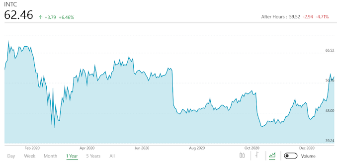
Starting with quarterly results, for the fourth quarter of 2020, Intel reported $20.0B in revenue, which is a drop of $0.2B over the year-ago quarter. Intel saw a very good Q4 a year ago, and while Q4’20 is once again their strongest quarter of the year, Intel’s momentum as a whole is starting to back off on a quarterly basis. More significantly, Intel’s net income has dropped 15% YoY, with Intel booking $5.9B there.
More...
-
01-22-21, 10:13 AM #10983
Anandtech: The Google Pixel 5: A Mini-Review - Small Package, Small Value?
The Pixel 5 is a change of tactic for Google, with the company opting to go the route of a lower-cost “premium” or high mid-range component configuration, rather than setting up the Pixel 5 as an all-out flagship phone. Given the company’s product release cadence over the years, always releasing new phones towards the end of the year, just around the corner of the spring next-gen releases. This schedule had always been a disadvantage for Pixel flagships, so maybe Google’s change of strategy here to go for the mid-range is a more sensible approach.
More...
-
01-22-21, 12:44 PM #10984
Anandtech: ASUS Pro WS WRX80E-SAGE SE WIFI Announced: A Motherboard for AMD Threadrip
In the world of crazy motherboard names, I think ASUS might have won with this one. The new ASUS Pro WS WRX80E-SAGE SE WIFI is a motherboard built for AMD’s upcoming Threadripper Pro processors featuring enough added clout to make the most of 128 lanes of PCIe 4.0._575px.png)
The extended-ATX (E-ATX) motherboard uses a transposed LGA4094 socket, capable of supporting the 64-core Threadripper Pro 3995WX at 280 W. The socket uses a 16 power stage VRM design with a massive finned heatsink designed to full air from the front of the motherboard to the back in line with the socket and the memory slots, ending in the rear panel which has its own air baffle. There are eight memory slots, enabling 512 GB or 1 TB of DDR4-3200.
The power delivery heatsink seems to be connected to the active chipset heatsink, which in turn has additional heatsinks for all three of the board’s PCIe 4.0 x4 M.2 slots. Other storage options include two U.2 ports, eight SATA ports, and a bundled Hyper M.2 card capable of supporting another four M.2 PCIe 4.0 x4 storage drives.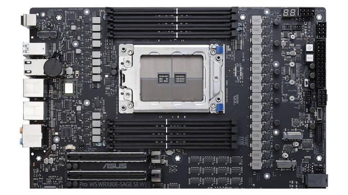
The board has seven full length supported PCIe 4.0 x16 slots for add-in cards, with these systems aimed at renderers and computational work that can add in additional compute cards. Additional controllers include an Intel X550-AT2 for dual 10 gigabit Ethernet, a baseband management controller (ASUS doesn’t say which one), and Wi-Fi 6 connectivity, likely enabled through Intel’s AX201 or AX210.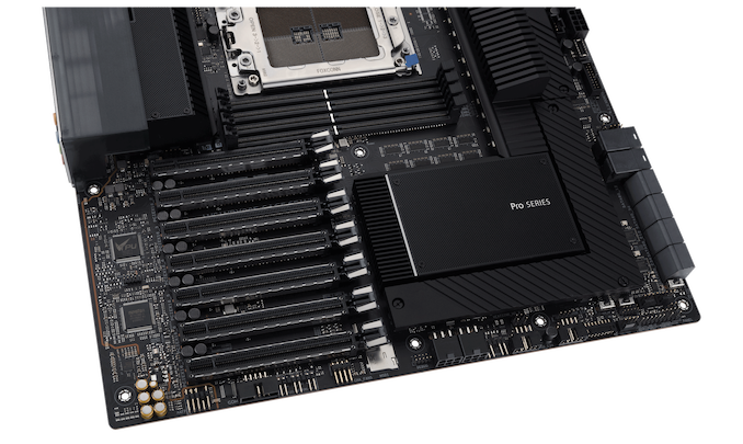
Port wise there are nine USB 3.2 Gen 2 ports each with 10 Gbps, and a single USB 3.2 Gen 2x2 Type-C port capable of 20 Gbps. For the front panel, there are two USB 3.2 Gen 2 connectors, as well as USB 3.2 Gen 1 and USB 2.0. Also on the board is BIOS flashback, CMOS reset, what looks like a Realtek ALC1220 audio codec, a COM header, and a wide array of 5-pin fan headers. ASUS’ custom TPU chipset is also onboard.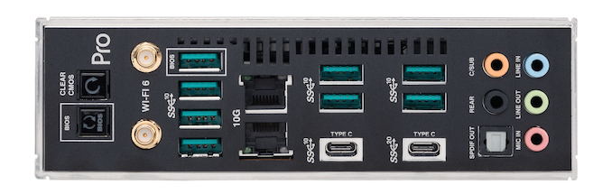
Users should also be aware that this board appears to take three 12V CPU power connectors, whereas most power supplies only take two. There are also two additional 6-pin PCIe connectors to provide power to the PCIe slots. The rear of the board contains a backplate to assist with board rigidity.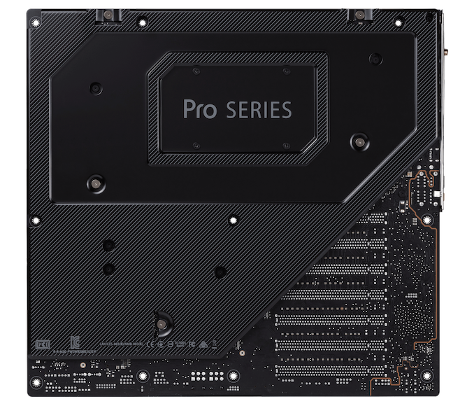
The ASUS Pro WS WRX80E-SAGE SE Wi-Fi is expected to be available in North America from March. Price is as-yet unknown.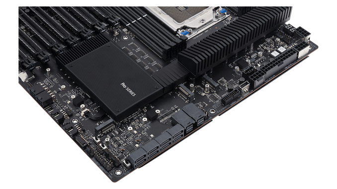
Related Reading:
Gallery: ASUS Pro WS WRX80E-SAGE SE WIFI Announced: A Motherboard for AMD Threadripper Pro_thumb.png)
_thumb.png)
_thumb.png)
_thumb.png)
_thumb.png)
_thumb.png)
More...
-
01-25-21, 12:48 PM #10985
Anandtech: The ASUS ROG Strix X570-E Gaming Motherboard Review
AMD's AM4 socket has been consistent throughout the entirety of its Ryzen processor's lifespan, and the latest Zen 3 processors are best suited for the X570 range of motherboards. Today it's time to see what the mid-range ASUS ROG Strix X570-E Gaming has to offer. Some of its main features include Intel 2.5 GbE and Wi-Fi 6, with dual PCIe 4.0 x4 M.2, with plenty of USB 3.2 G2 connectivity. The ROG Strix X570-E Gaming looks strong and we examine it to see how it stacks up.
More...
-
01-26-21, 08:09 AM #10986
Anandtech: AMD Ryzen 9 5980HS Cezanne Review: Ryzen 5000 Mobile Tested
Since AMD’s introduction of its newest Zen 3 core for desktop users, the implementation for notebooks and mobile users has been eagerly awaited. In a single generation, on the same manufacturing process, AMD extracted +19% more performance per clock (we verified), so for any system that is power limited, extra performance is often very well received. AMD announced its new Ryzen 5000 Mobile processor family at the start of the year, with processors from 15W to 45W+ in the pipeline, and the first mobile systems coming to market in February. AMD sent us a peak example of Ryzen 5000 Mobile for today’s review, the 35W Ryzen 9 5980HS, as contained in the ASUS ROG Flow X13.
More...
-
01-26-21, 08:09 AM #10987
Anandtech: Intel Iris Xe Video Cards Now Shipping To OEMs: DG1 Lands In Desktops
Following plans first unveiled last year during the launch of their DG1 GPU, Intel sends word this morning that the first Iris Xe video cards have finally begun shipping to OEMs. Based on the DG1 discrete GPU that’s already being used in Intel’s Iris Xe MAX laptop accelerators, the Iris Xe family of video cards are their desktop counterpart, implementing the GPU on a traditional video card. Overall, with specifications almost identical to Xe MAX, Intel is similarly positioning these cards for the entry-level market, where they are being released as an OEM-only part.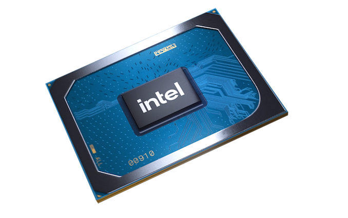
As a quick refresher, the DG1 GPU is based on the same Xe-LP graphics architecture as Tiger Lake’s integrated GPU. In fact, in broad terms the DG1 can be thought of as a nearly 1-to-1 discrete version of that iGPU, containing the same 96 EUs and 128-bit LPDDR4X memory interface as Tiger Lake itself. Consequently, while DG1 is a big first step for Intel – marking the launch of their first discrete GPU of the modern era – the company is planning very modestly for this generation of parts.
The first DG1 GPUs were shipped in the fall as part of Intel’s Iris Xe MAX graphics solution for laptops. At the time, Intel also indicated that a desktop card for OEMs would also be coming in 2021, and now, right on schedule, those desktop cards have begun shipping out.Intel Desktop GPU Specification Comparison Iris Xe
dGPUTiger Lake
iGPUIce Lake
iGPUKaby Lake
iGPUALUs 640
(80 EUs)768
(96 EUs)512
(64 EUs)192
(24 EUs)Texture Units 40 48 32 12 ROPs 24? 24 16 8 Peak Clock 1650MHz? 1350MHz 1100MHz 1150MHz Throughput (FP32) 2.11 TFLOPs 2.1 TFLOPs 1.13 TFLOPs 0.44 TFLOPs Geometry Rate
(Prim/Clock)2 2 1 1 Memory Clock LPDDR4X-4266? LPDDR4X-4266 LPDDR4X-3733 DDR4-2133 Memory Bus Width 128-bit 128-bit
(IMC)128-bit
(IMC)128-bit
(IMC)VRAM 4GB Shared Shared Shared TDP ~25W? Shared Shared Shared Manufacturing Process Intel 10nm SuperFin Intel 10nm SuperFin Intel 10nm Intel 14nm+ Architecture Xe-LP Xe-LP Gen11 Gen9.5 GPU DG1 Tiger Lake
IntegratedIce Lake Integrated Kaby Lake Integrated Launch Date 01/2021 09/2020 09/2019 01//2017
Overall, Intel is taking a very OEM-centric approach to their DG1 products, and that goes for both laptops and the desktops. Even the desktop Iris Xe cards won’t be sold as retail – as entry-level cards, they are unlikely to fly off of shelves – and instead are only being sold to OEMs for use in pre-built systems. And even then, the cards were co-designed with ecosystem partners – of particular note, ASUS – rather than Intel building and shipping out their own video cards. So by desktop video card standards, Intel is being somewhat hands-off at the moment.
In a curious twist, the desktop cards will have slightly lower specifications than the laptop parts. While I’m still waiting to hear what the TDPs and final clockspeeds will be, Intel’s announcement confirms that the Iris Xe cards will only ship with 80 of 96 EUs enabled, rather than being fully-enabled in the case of the laptop parts. Given that this is an entry-level part, any further drop in performance isn’t doing the part any favors, but at the same time it was never going to be a speed-demon to begin with. At any rate, given that no chip has perfect yields, we now know where salvaged DG1 chips are going.
Meanwhile, like their laptop counterparts, the Iris Xe desktop cards will ship with 4GB of LPDDR4X memory. And though Intel didn’t send over any pictures in advance, we know that the cards will ship with three display outputs – presumably using a mix of HDMI and DisplayPorts.
As for Intel’s target market, the company is targeting what they’re calling the “high-volume, value-desktop market.” Notably, unlike the Iris Xe MAX launch, Intel’s (admittedly brief) news release doesn’t spend much time focusing on the cards as a secondary accelerator, and instead are promoting these as a superior solution over existing graphics options. Given the focus on things like AV1 decoding, HDR support, and deep learning inference performance, I’m assuming that these will primarily be showing up in Atom (Gemini Lake Refresh) systems. Though it may also show up in low-end Comet Lake Celeron and Pentium systems, where vendors are looking to add a few more display ports and take advantage of the additional hardware accelerator blocks for things like video encoding, similar to how Intel positioned Iris Xe MAX for laptops.
Finally, given the OEM-centric nature of today’s launch, Intel isn’t publishing any specific availability dates for their Iris Xe video cards. But we expect that they’ll begin showing up in short order.
More...
-
01-26-21, 10:11 AM #10988
Anandtech: Sony Launches Xperia PRO 5G ... for $2499
Last year in February Sony had launched the Xperia 1 II, as well as teasing a sibling device called the Xperia PRO. This latter variant of the phone was meant to be a professional variant of the Xperia 1 II, in a more rugged form-factor, as well as integrating a HDMI input port.
Today, almost a whole year later, Sony is ready to finally to launch the Xperia PRO 5G, with availability starting today at a staggering price tag of $2499.
The peculiarity about the Xperia PRO 5G are two key features: a HDMI input port alongside the usual USB-C port, as well as additional mmWave 5G connectivity in the form of four antennas, more than the usual two or three we find in other consumer models.

Sony is trying to position the Xperia PRO as a professional accessory for broadcast video, where the phone directly attaches to your camera feed via HDMI and is able to directly upload to the internet. It’s a very niche use-case, however Sony is trying to replace several discrete devices in one: The Xperia PRO can serve simultaneously as a high-quality monitor, and actually outperform most other dedicated camera monitors out there thanks to its 6.5” 3840 x 1644 HDR OLED screen, as well as serving as a cellular video streamer, a kind of device that usually alone goes for $1000 to $1500.
Furthermore, Sony is doing a lot of fanfare about the phone’s 4 mmWave antennas and how it’ll be able to achieve much better, stable, and uniform reception compared to other devices in the market which employ only 2 or 3 antennas. The caveat here is of course that this will only ever get used when under actual mmWave coverage, which is still a very limited number of locations in the US. Of course, the phone will fall back to sub-6GHz 5G and LTE whenever there’s no mmWave coverage.
So, while the $2499 price tag might sound absolutely outrageous at first, it’s not much more expensive than other discrete solutions such as a dedicated monitor as well as competing, feature poorer cellular streaming devices. Where I do think Sony dropped the ball here is in terms of software features: the Xperia PRO lacks more commonly found features in dedicated monitors such as wave forms or vector scopes, and also lacks any kind of camera control or status features, even with Sony’s own line-up of cameras. For the device being now launched almost a whole year after its initial announcement, that’s extremely disappointing. During the Q&A briefing, it seems that Sony is aware of these features missing, but offered no concrete answers on whether they’ll continue to evolve the product from a software standpoint.
The Xperia PRO is otherwise feature identical to an Xperia 1 II – including the Snapdragon 865 SoC, the triple-camera setup, screen, and battery size, though DRAM and storage are upped to 12GB and 512GB. Furthermore, Sony says that the Xperia PRO is only launching in the US for $2499, with no current plans for availability in other markets.
Related Reading:- Sony Announces New Xperia 1 II Flagship, Teases Xperia PRO
- Sony Announces Xperia 5 II: 120Hz Full-Fledged Small Phone
More...
-
01-26-21, 10:11 AM #10989
Anandtech: AMD's Ryzen 5000 Lucienne: Not Simply Rebranded Ryzen 4000 Renoir
AMD came in for some harsh criticism when it announced that its new Ryzen 5000 Mobile U-series processors would not all be using its latest core design. At the product announcement, we were told that some of the U-series processors would be based on the previous Zen 2 generation, and this was mainly for partners to take advantage of the new naming scheme but also reuse designs with the same ballpark performance. A number of tech enthusiasts (including myself, I have to say) scoffed at this as it made the whole system complex. It’s still complex, but we’ve come to understand that these latest Zen 2 based mobile processors also include a whole raft of updates that make them a better version of what they are.
To simplify things I’m going to call these products by their AMD codenames. The older Zen 2 processors are called Renoir, and the newer Zen 2 processors are called Lucienne. Here is a list of the new Ryzen 5000 U-Series, with Lucienne listed in yellow.
Renoir, for all intents and purposes, was a very successful product for AMD. Placed in the Ryzen 4000 Mobile series, it became the bedrock of AMD’s mobile portfolio and has been installed in around 100 design wins since it came to market. Lucienne on the other hand is a minor player in the latest Ryzen 5000 Mobile series. It doesn’t have the updates that the new Zen 3 cores have, but we have since learned that on the power side of things, rather than being a copy of Renoir, it is almost certainly Renoir Plus.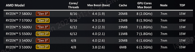
What Lucienne brings to the table over Renoir comes in discrete categories.
Memory Controller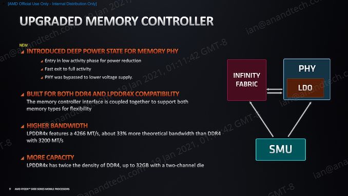
The memory controller in Lucienne is now able to decouple its voltage from the cores and enter a lower power state when not in use or for low bandwidth reasons. This ultimately saves power, and AMD has enabled it to bypass particular voltage indicators to help it stay in the low voltage state. Aside from the cores and the graphics, the other two consumers of power inside a mobile processor is the internal communications and the external communications, of which the memory controller falls under the latter. AMD has also put into place a system by which the memory controller can wake to a full bandwidth state faster than before, enabling better responsivity from those deep sleep states.
On top of this, the memory controller can now support double the capacity of memory from Renoir: up to 64 GB of DDR4-3200, or up to 32 GB of LPDDR4X-4267. Using DDR4 means the system can have more peak memory, as well as being user adjustable, however LPDDR4X trades those in for faster bandwidth overall (68.4 GB/s vs 51.2 GB/s).
Per-Core Voltage Control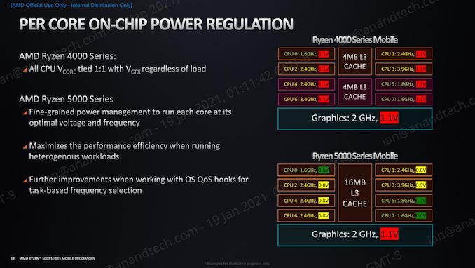
In similar circumstances to the memory controller, having voltage control of each individual core in a mobile processor is one angle to both maximize performance when needed and minimize power loss when idle. In Renoir, all of the cores can adjust their frequency, but they all had to run at the same voltage. Lucienne changes that such that each core can adjust its voltage independently, enabling a finer grained power management and a more optimal power-efficient system. There are also additional hooks that operating systems can use if it knows high performance cores are needed in advance.
Preferred Core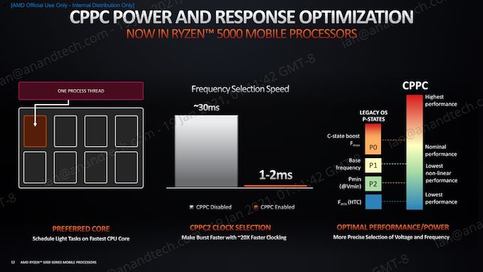
When we speak about turbo, historically it has been assumed that any core can reach the highest single core turbo frequency, and that the workload is sometimes shifted between cores to help with thermal management. When a system uses a preferred core however, it means that a system could be optimized for that specific core, and more performance extracted. AMD introduced its Preferred Core technology on the desktop two generations ago, and now it comes to the mobile processors. One core out of the eight on Lucienne silicon will be designated the best core, and through an OS driver (default in Windows) all workloads will be placed on that core preferentially.
Frequency Ramp
One of the features that tie all of this together is how quickly a core can move from idle to peak performance and back again. If a system takes too long to ramp up to speed, or ramp back down, then responsiveness and power is lost. A typical modern system is expected to ramp up from idle to peak frequency within two frames at 60 Hz, or 32 milliseconds, however the latest systems from AMD and Intel have done it much faster, often within 16 ms. AMD’s enhanced clock gating technology is now enabling Lucienne to reduce that down to 1-2 milliseconds. This means that a system could easily ramp up and down between each keystroke on a keyboard, supplying immediate responsiveness to a user while keeping the total power use down. In the 16-32 millisecond regime, typing on a keyboard may have meant a core being active almost continuously, however making this change faster affords a lot of power savings through these transitions.
Continuous Performance Levels
The legacy way for an operating system to command performance is through performance states, or P-states. In this instance the OS would request a specific level of power and performance from the processor based on its detected workload, and the processor would respond. This was originally implemented during a time when turbo was first coming to modern processors, and workload analysis was better done through the operating system. Now we can do this level of monitoring on the processor directly, and through an OS driver (already part of Windows), with system support that level of frequency control can be passed back down to the processor. The processor also gets an effective continuous distribution of performance, rather than discrete P-states.
While Renoir had P-states, Lucienne gets the benefit of CPU-level performance requests.
Faster Integrated Graphics
With the additional power control elsewhere on the core, how the power delivery works to the integrated graphics was also adjusted to allow for better regulation and ultimately a lower minimum voltage. Through firmware AMD has enabled a frequency sensitive prediction model that allows the GPU to adjust its voltage and frequency based on its dynamic energy management. Coupled with the better regulation and the power budget balancing done between CPU, interconnect, DRAM, and the GPU, more power budget is available for the GPU. For Lucienne, this means +150 MHz on the peak IGP speeds compared to Renoir.
But I thought Lucienne Silicon was the same as Renoir Silicon?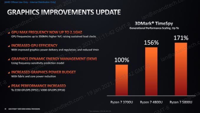
Slide shows Cezanne numbers, but applies to Lucienne as well
This is the big question. We asked AMD if Lucienne was the same stepping of Renoir, and the answer was not exactly committal in one direction or the other. The simple answer is yes, however AMD wants to make clear that substantial changes were made to firmware and manufacturing that means that despite the transistor layout being identical, there are features of Lucienne that would never have worked in Renoir without the changes that have been made.
So while yes it is the same silicon layout and floorplan, some of these features weren’t possible in Renoir. AMD built in these features perhaps knowing that they couldn’t be enabled in Renoir, but sufficient changes and improvements at the manufacturing stage and firmware stage were made such that these features were enabled in Lucienne. More often than not these ideas often have very strict time windows to implement, and even if they are designed in the hardware, there is a strict cut-off point by which time if it doesn’t work as intended, it doesn’t get enabled. Obviously the best result is to have everything work on time, but building CPUs is harder than we realize.
Sometimes I wonder how we ever get these rocks powered by lightning to work in the first place.
More...
-
01-26-21, 12:56 PM #10990
Anandtech: NVIDIA Launches Server Certification Program, Offering Direct Technical Su
While a good deal of NVIDIA’s success in servers over the last decade has of course come from their proficient GPUs, as a business NVIDIA these days is much more than a fabless GPU designer. With more software engineers than hardware engineers on staff, it’s software and ecosystem plays that have really cemented NVIDIA’s position as the top GPU manufacturer, and created a larger market for their GPUs. At the same time, it’s these ecosystem plays that have allowed NVIDIA to build a profit-printing machine, diversifying beyond just GPU sales and moving into systems, software, support, and other avenues.
To that end, NVIDIA this morning is formally rolling out a new ecosystem play aimed at high-end deep learning servers, which the company is branding as NVIDIA-Certified Systems. Soft-launched back in the fall, today the company is giving the program a more proper introduction, detailing the program and announcing some of the partners. Under NVIDIA’s plan, going forward customers can opt to buy NVIDIA-Certified systems if they want an extra guarantee on system performance and reliability, as well as opt in to buying support contracts to get access to direct, full-stack technical support from NVIDIA.
Conceptually, the certification program is rather straightforward, due in large part to its hardware requirements. Systems first need to be using NVIDIA’s A100 accelerators, along with Mellanox Ethernet adapters and DPUs. Or in other words, the servers already need to be using NVIDIA silicon where available. OEMs can then submit systems meeting these hardware requirements to NVIDIA, who will test the systems across multiple metrics, including multi-GPU and multi-node DL performance, network performance, storage performance, and security (secure boot/root of trust). Systems that pass these tests can then be labeled as NVIDIA-Certified.
Those certified systems, in turn, are eligible for additional full-stack technical support through NVIDIA and the OEM. Customers can opt to buy multi-year support contracts, which entitles them to support through the OEM and NVIDIA. NVIDIA essentially assumes responsibility for all software support above the OS, including their hardware drivers, CUDA, their wide collection of frameworks and libraries, and even major open source libraries like TensorFlow. The latter is what makes NVIDIA’s support proposition particularly valuable, as they’re essentially committing to helping customers with any kind of GPU or deep learning-related software issue.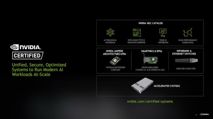
Of course, that support won’t come for free: this is where NVIDIA will be making their money. While NVIDIA is not charging OEMs for certification (so there’s no additional certification tax baked into the hardware), support contracts are priced based on the number of GPUs. In one example, NVIDIA has stated that a 3 year support contract for a dual-A100 system would be $4,299, or about $715 per-year per-GPU for support. So one can imagine how quickly this ratchets up for larger 4 and 8 way A100 systems, and then again for multiple nodes.
For NVIDIA and its OEM partners, the creation of a certification program is a straightforward way to try to further grow the market for deep learning servers, especially for mid-sized businesses. The market for AI hardware has been booming, and NVIDIA wants to keep it that way by making it easier for potential customers to use their wares. NVIDIA already has the top-end of the market covered in this respect with their direct relationships with the hyperscalers – and by extension their small-cap cloud computing customers – so a hardware certification program fills the middle tier for organizations that are going to run their own servers, but aren’t going to be a massive customer that gets personalized attention.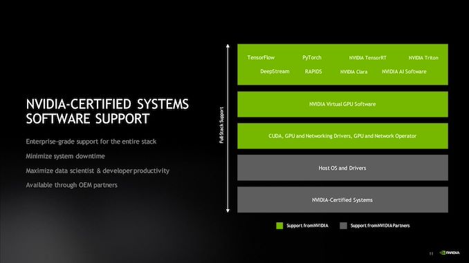
As for those customers, NVIDIA’s server certification and support programs are designed to eliminate (or at least mitigate) the risks of making significant investments into NVIDIA hardware. That means being able to buy a system where the vendor (in this case the duo of NVIDIA and the OEM) can vouch for the performance of the system, as well as guarantee it will be able to properly run various AI packages, such as NVIDIA’s NGC catalog of GPU-optimized and containerized software.
Altogether, NVIDIA is launching with 14 certified systems, with the promise of more certified systems to come. For the first wave of systems, participating OEMs include Dell, Gigabyte, HPE, Inspur, and Supermicro, all of whom are frequently participants in new NVIDIA server initiatives.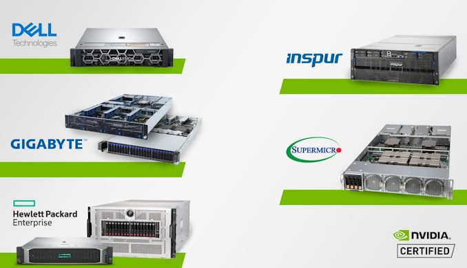
With all that said, NVIDIA’s server certification program is unlikely to significantly change how things work for most of the company’s customers; but it’s a program that seems primed to address a specific niche for NVIDIA and its OEM partners. For companies that are interested in GPU computing but are looking for a greater degree of support and certainty, this would address those needs. Which, to bring things full circle, it’s exactly by addressing those sorts of needs with ecosystem plays like server certification that NVIDIA has been so successful in the server GPU market over the last decade.
Gallery: NVIDIA-Certified Systems Press Deck


Source: NVIDIA
More...


 Quote
QuoteThread Information
Users Browsing this Thread
There are currently 21 users browsing this thread. (0 members and 21 guests)


Bookmarks