

Results 11,471 to 11,480 of 12091
Thread: Anandtech News
-
04-11-22, 06:15 PM #11471
Anandtech: Intel Opens D1X-Mod3 Fab Expansion; Moves Up Intel 18A Manufacturing to H2
Intel for the last few years has been undergoing a major period of manufacturing expansion for the company. While the more recent announcements of new facilities in Ohio and Germany have understandably taken a lot of the spotlight – especially given their importance to Intel’s Foundry Services plans – Intel has been working even longer on expanding their existing facilities for their own use. The company’s development of next-generation EUV and Gate-All-Around-style transistors (RibbonFET) not only requires creating and refining the underlying technology, but it also just flat out requires more space. A lot of it.
To that end, Intel today is holding a grand opening in Oregon for the Mod3 expansion of D1X, the company’s primary development fab. The expansion, first announced back in 2019, is the third such mod (module) and second expansion for Intel’s main dev fab to be built since D1X’s initial construction in 2010. And in keeping with tradition for Intel fab launches and expansions, the company is making something of an event of it, including bringing Oregon’s governor out to show off their $3 Billion investment.
But fanfare aside, the latest mod for the fab is a genuinely important one for Intel: not only does it add a further 270,000 square feet of clean room space to the facility – expanding D1X by about 20% – but it’s the only fab module that’s big enough to support the High Numerical Aperture (High NA) EUV tool that Intel will be using starting with its 18A process. ASML’s forthcoming TWINSCAN EXE:5200 EUV tool is designed to be their most powerful yet, but it’s also quite a bit larger than the NXE 3000 series EUV tools Intel is using for their first generation EUV processes (Intel 4/3). It’s so big that D1X’s ceiling is too low to fit the machine, never mind support its weight.
More...
-
04-12-22, 10:25 AM #11472
Anandtech: Broadcom Launches Wi-Fi 7 Portfolio for Access Points and Client Devices
The last few years have seen heightened consumer focus on wireless networking. The industry has also been quite busy, enabling the operation of Wi-Fi 6 (802.11ax) in the 6GHz band with Wi-Fi 6E. In parallel, the 802.11 Working Group had started work on 802.11be with a focus on extremely high throughput (EHT). Wi-Fi 7 is set to become the consumer-facing moniker for 802.11be.
802.11be aims to achieve high throughput primarily through a combination of three aspects:
- Support for up to 16 spatial streams
- Support for 320MHz-wide channels (with operation in 2.4 GHz, 5 GHz, and 6 GHz bands)
- Support for 4096-QAM (4K-QAM) resulting in better utilization of available spectrum (a faster modulation / coding scheme).
Theoretically, these aspects allow for up to around 46 Gbps of wireless throughput. 802.11be also aims to enable usage of Wi-Fi for real-time applications by including features for low-latency communications such as Multi-link operation (MLO). This allows a client and an access point to simultaneously communicate over multiple channels that might even belong to different bands. Interference and co-existence with non-Wi-Fi users of the same spectrum is handled using automatic frequency coordination (AFC).
A number of additional features targeting these two thrust areas are under consideration for the final standard. However, multiple silicon vendors have already started introducing silicon supporting variations of the aspects included in the first 802.11be draft specifications.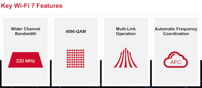
Mediatek was one of the first vendors to demonstrate working 802.11be-compliant silicon earlier this year. Though Mediatek indicated that the products would be marketed under the Filogic lineup, concrete technical details and part numbers were not announced. At MWC 2022, Qualcomm provided details of their 802.11be client silicon targeting mobile devices. The FastConnect 7800 is expected to become available in H2 2022, and integrates Bluetooth 5.3 support with key Wi-Fi 7 features.
Broadcom is announcing a comprehensive portfolio of products targeting various Wi-Fi 7 markets today.
The table below summarize the key features of the products targeting access points. All of these support 4K-QAM and Multi-Link Operation.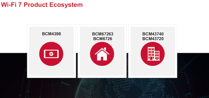
The AP products support AFC in order to ensure that 6GHz range is not affected (the APs are mandated to receive regularly scheduled clearance from a central authority to prevent interference with 6 GHz spectrum users). Broadcom has applied to be an AFC operator and will offer AFC service with their chips. This will use Open AFC code. Broadcom also believes a vibrant Wi-Fi 7 ecosystem requires an AFC service that the device makers can use independent of the chip vendor. Organizations such as the Wi-Fi Alliance, and Wireless Broadband Alliance have applied to be AFC operators, with Open AFC already gaining traction in this.Broadcom 802.11be (Wi-Fi) Access Point Radios Specifications BCM67263 BCM6726 BCMN43740 BCMN43720 Target Market Residential Wi-Fi APs Enterprise Wi-Fi APs Operational Band 6 GHz 2.4 GHz (or) 5 GHz (or) 6 GHz Stream Count 4 2 Max. Channel Width 320 MHz 160 MHz 320 MHz 160 MHz PHY Rate 11.5 Gbps 5.75 Gbps 11.5 Gbps 2.88 Gbps
Tying these together in Broadcom's Wi-Fi 7 router reference design is the BCM4916 network processor. This ARM v8-compatible quad-core SoC includes a dual-issue Runner packet processor (DI-XRDP), an integrated NBASE-T (up to 10G) Ethernet PHY for WAN or LAN, four integrated 1GbE PHYs, three USXGMII interfaces, multiple USB ports, and a 32-bit DDR3/DDR4 DRAM interface.
The quad-core CPU is a custom Broadcom design with 64KB of L1 cache and 1MB of L2 cache, providing up to 24K DMIPS horsepower. Without the knowledge of exact clock speeds, it is difficult to compare against the standard Cortex cores from ARM. Based on the DMIPS number, this appears to slot in-between a Cortex-A53 and an A57, but does not include the ARM v8.2 features of the A55.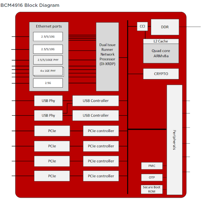
Broadcom's customers can play around with the radio configuration in the above design to create products at different price points. Tri-band support becomes compulsory in Wi-Fi 7. The extremely high throughput enabled by this means that 10G support on the WAN/LAN side and NBASE-T support on the LAN front will become the de-facto standard for routers and APs in the coming years.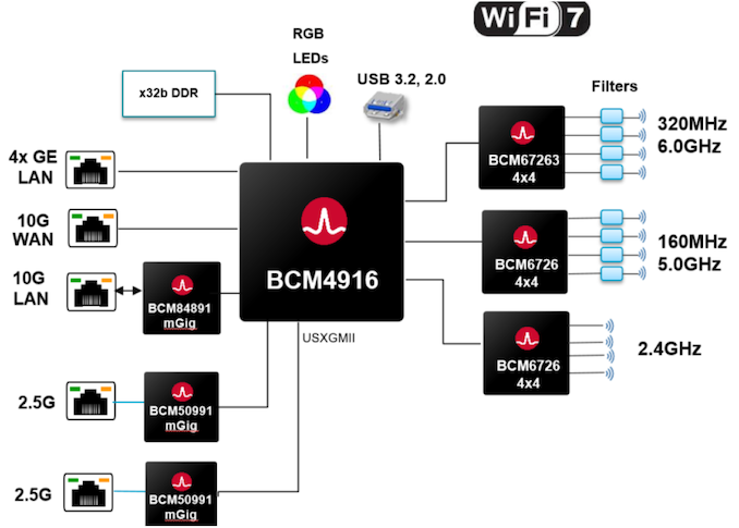
Broadcom is also introducing the BCM4398 - an integrated Wi-Fi 7 and Bluetooth 5 combo chip targeting smartphones and other mobile applications. It supports two streams of Wi-Fi 7, channel width of up to 320 MHz, and a 6.05 Gbps PHY rate. On the client side, one of the key user-visible updates is low-latency operation. Broadcom claims that the BCM4398 can achieve sub-millisecond latencies for lightly congested environments in the 6 GHz band. The client multi-link operation feature can keep both uplink and downlink latencies between 5 and 10ms in situations where both 5 and 6 GHz bands are highly congested. This provides determinism for AR/VR knowing that worst case latencies will be down to a few milliseconds even during heavy congestion.
Broadcom is the first vendor to announce a complete portfolio of Wi-Fi 7 products, with sampling for key customers already in progress. The new products should give end-consumers a taste of the values delivered by Wi-Fi 7 for different applications a few quarters from now.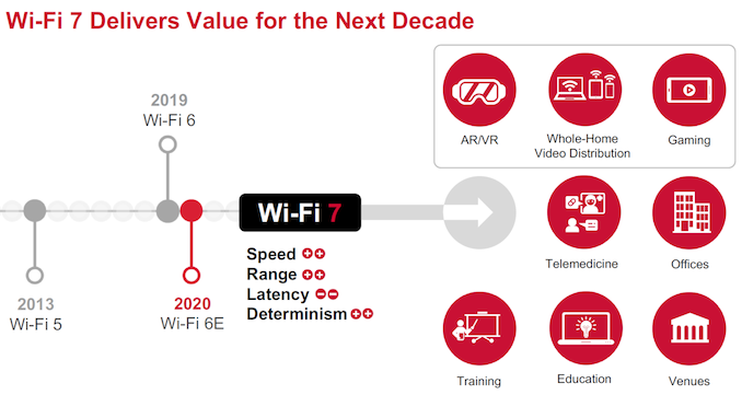
Gallery: Broadcom Launches Wi-Fi 7 Portfolio for Access Points and Client Devices


More...
-
04-13-22, 12:57 PM #11473
Anandtech: The PowerWalker VI 1500 CSW UPS Review: Trying For True Sinewave on a Budg
While Uninterruptible Power Supplies are hardly a new thing in the PC space, the tried-and-true battery backups for desktop PCs have been undergoing a resurgence in popularity in recent years. Improvements in power delivery technology such as GaNs have been reducing costs and improving reliability, and meanwhile lithium-ion batteries, with their much greater energy density/lower volume, are starting to make inroads on the UPS market as well. All the while, with laptops outselling desktops in the consumer PC market, a PC that doesn't shut itself down during a power outage is becoming the norm, rather than the exception. So what better time is there to take a look at UPSes?
To kick off our nagual UPS review, we're starting with a 1500VA unit from BlueWalker. BlueWalker is a company that originates from Germany and specializes on the design and marketing of power-related equipment. The company was founded in 2004, making it one of the oldest household UPS/AVR manufacturers that still exist to this date.
BlueWalker is marketing their retail products under the PowerWalker brand name and has a very wide portfolio of both hardware and software products available. For today’s review, we are taking a look at the PowerWalker VI 1500 CSW, a 1500VA/900W UPS that boasts true sinewave output. Of particular interest with this UPS is the price: true sinewave units have historically carried a significant price premium, but BlueWalker isn't charging nearly the premium as true sinewave UPSes from other major manufacturers, making the PowerWalker VI 1500 CSW a much cheaper UPS. But can it live up to the same power delivery expectations without the same wallet-busting cost? Let's find out.
More...
-
04-20-22, 07:41 AM #11474
Anandtech: The FSP Hydro PTM Pro 1200W PSU Review: Improving on the Tried and True
Today we are having a look at one of the best PSUs FSP has to offer, the Hydro PTM Pro 1200W. FSP is an OEM who usually builds PSU platforms for other companies, however the Hydro PTM Pro is a PSU that they design and produce themselves, making it interesting to see what the company has to offer directly to the retail market.
More...
-
04-22-22, 02:04 PM #11475
Anandtech: TSMC Roadmap Update: N3E in 2024, N2 in 2026, Major Changes Incoming
Taiwan Semiconductor Manufacturing Co. has solid plans for the next few years, but the foundry's manufacturing technology design cycles are getting longer. As a result, to address all of its clients' needs, the company will have to keep offering half-nodes, enhanced, and specialized versions of its fabrication processes.
TSMC's success in the last 20 years or so was largely conditioned by the company's ability to offer a new manufacturing technology with PPA (power, performance, area) improvements every year and introduce a brand-new node every 18 – 24 months while maintaining predictably high yields. But as complexity of modern fabrication processes gets to unprecedented levels, it is getting much harder to keep the pace of innovation while also sustaining predictable yields and simple design principles.
With TSMC's N3 node, the gap between N5 (5 nm-class) ramp up and N3 (3 nm-class) ramp up will increase to around 2.5 years, which may pose some challenges to the foundry's key customer, Apple. The good news is that N3's follow up, N3E, seems to be coming in ahead of schedule. Meanwhile, with N2, the cadence is set to stretch to about three years, which largely means a strategic shift in TSMC's strategy of node development.
N3E: An Improved 3nm Node Pulled In (Almost)
TSMC's N3 is set to bring in full node improvements over N5, which includes 10% ~ 15% more performance, 25% ~ 30% power reduction, and an up to 1.7X higher transistor density for logic. To do so, it will use more than 14 extreme ultraviolet (EUV) lithography layers (N5 uses up to 14, and N3 is expected to use even more) and will introduce certain new design rules for deep ultraviolet lithography (DUV) layers.
TSMC is set to start ramping up production of chips using its N3 node in the second half of the year and will deliver the first commercial batch to a client (or clients) in early 2023, which is when it will receive the first N3 revenue.Advertised PPA Improvements of New Process Technologies
Data announced during conference calls, events, press briefings and press releasesTSMC N7
vs
16FF+N7
vs
N10N7P
vs
N7N7+
vs
N7N5
vs
N7N5P
vs
N5N3
vs
N5Power -60% 37%
-
~17%0.55x
-45%
(1.8x)
-0.58x
-42%
(1.7x)Volume
ManufacturingQ2 2019 Q2 2020 2021 H2 2022
While TSMC's N3 process technology was designed both for high-performance computing (which is a term that TSMC uses to describe applications like CPUs, GPUs, FPGAs, ASICs, etc.) and smartphones in mind, there is evidence that the node has a rather narrow process window, which would make it hard for chip developers to hit desired specifications. This is a problem as it increases time-to-yield and ultimately lowers margins. In an apparent bid to tackle the issue, TSMC has developed N3E version of the technology that widens process window and provides improvements over N5.
"N3E will further extend our N3 family with enhanced performance, power, and yield," said C. C. Wei, chief executive of TSMC.
Originally, TSMC planned to start high-volume manufacturing (HVM) using N3E about a year after N3 (i.e., in Q3 2023), but in the recent months a rumor emerged that TSMC was pulling in HVM of N3E by about a quarter due to better than expected test production runs. During its most recent conference call, TSMC confirmed that N3E's progress was ahead of schedule and that it was considering pulling in mass production using this technology, but did not elaborate about exact plans.
"Our N3E result is quite good," said the head of TSMC. "The progress is ahead of our schedule. And pull-in, yes, we are considering that. So far, I still did not have a very solid data to share with you that how many months we can pull in. But yes, it is in our plan."
Keeping in mind that chip developers have their own schedules for their designs, it is unlikely that all of them will be able to take advantage of earlier N3E ramp since their chips have to pass all the pre-production iterations as well. Nonetheless, better-than-expected N3E progress is a good sign in general, especially considering the fact that TSMC's N3 family will have to serve the industry for quite a long time.
N2: Expect First Chips in 2026
In fact, N3 and its evolutionary iterations will remain TSMC's leading-edge offerings till late 2025 because the company's N2 (2 nm-class) schedule looks quite conservative.
When TSMC first talked about its N2 in August 2020, it did not reveal many details about the technology (by now we know that it adopts gate-all-around [GAA] transistor structure) or its schedule, but indicated that it would build a brand-new fab near Baoshan, Hsinchu County, Taiwan, for this node (some sources call this new facility Fab 20). Taiwanese authorities approved the construction plan in mid-2021 and that plan included breaking ground in early 2022 (earlier this year TSMC's board of directors indeed accepted capital appropriations for a new fab construction), so we believe that the shell is being built as we speak.
Shell construction usually takes a year or a little more, then equipment installation takes over a year as well, so we expect the first phase of Fab 20 to be ready by mid-2024 at the latest. TSMC expects to start risk production using its N2 technology in late 2024 and then initiate HVM towards the end of 2025, which means that the gap between the initial N3 ramp in Q3 2022 and initial N2 ramp in Q4 2025 will be about three years.
"Our progress so far today for the N2 is on track," said Mr. Wei. "All I want to say is, yes, at the end of 2024, [N2] will enter the risk production. 2025, it will be in production, probably close to the second half or the – or the end of 2025. That is our schedule."
Considering how long modern chip production cycles are, it is safe to say that the first N2 chips made by TSMC will arrive in consumer devices no sooner than early 2026.
But perhaps TSMC's public disclosures about N2 and Fab 20 are too conservative. Analysts from China Renaissance Securities seem to be more optimistic about Fab 20 readiness than TSMC is, which may be an indicator that the foundry could pull-in N2 HVM by a quarter or even two if the fabrication process meets its performance, power, and yield goals.TSMC's New Node Introduction in Recent Years N7 N7P N5 N5P N3 N3E N2 Transistor Type FinFET FinFET FinFET FinFET FinFET FinFET GAA FET Risc Production ? ? ? ? 2021 2022 Late 2024 Volume
ManufacturingQ2 2018 Q2 2019 Q2 2020 Q2 2021 Q3 2022 Q2/Q3 2023 Late 2025
"We also see more clarity around TSMC's N2 expansion schedule in Fab 20 (Hsinchu)," Sze Ho Ng, an analyst with China Renaissance Securities, wrote in a report for clients. "Tool move-in is expected to start by end-2022, based on company plans, ahead of risk production in late 2024E with Intel (client PC Lunar Lake's graphic 'tiles', while the CPU 'tiles' are fabbed using Intel’s 18A) and Apple being the anchor customers for dedicated capacity support."
Meanwhile, pulling in a node from Q4 2025 to Q3 2025 when alpha customers already set their plans for 2025 may not make a lot of sense, but we will certainly see how things work out with N2.
More N3 Iterations
This year, TSMC's customers that need a leading-edge fabrication process will use the company's N4 technology, which belongs to the N5 family (along with N5, N5P, N4P, and N4X). Essentially, this means that an N5 node will remain TSMC's most advanced offering for three consecutive years.
N3 nodes will also have to serve TSMC's clients for another three years (2023, 2024, 2025), so we are going to see several iterations of this process. So far, TSMC has formally confirmed N3E and N3X (which is another performance-oriented manufacturing technology akin to N4X aimed primarily at CPUs and datacenter ASICs), but I would expect more N3-derived nodes to come to address mainstream SoCs in 2024 ~ 2025.
Keeping in mind that TSMC's FinFET-based N3 will have to stay competitive against GAA-based Samsung's 3GAP and 2GAE/2GAP in 2023 ~ 2025 and Intel's 20A (RibbonFET + PowerVia) in 2024 and 18A (High-NA EUV) in 2025, TSMC's engineers will have to be quite creative with their N3 enhancements.
On the foundry side of things, TSMC will remain ahead of its rivals for quite a while since Intel is not expected to invest significantly in its IFS-dedicated capacity before 2025 (so its 20A and 18A capacities for IFS customers will likely be limited), whereas Samsung Foundry is traditionally behind TSMC when it comes leading-edge capacity and prefers to prioritize its parent company and strategic clients (e.g., Qualcomm). But formal process technology leadership is what TSMC's engineers will have to maintain with N3 and it will be uneasy to do considering how aggressive Intel and Samsung are.
Changes Are Coming
Evidently, TSMC's brand-new process development and ramp up cadence has increased to two-and-a-half years with N3 and will increase to three years with N2, which may be considered as a major slowdown by its key customers. Meanwhile, potential pull-in of N3E is a good sign which shows that the company can make its intra-node advancements fairly quickly. Hence, the main question is how significant will TSMC's intra-node advancements be going forward. This is a question that only time will answer.
In the meantime, it looks like with TSMC's three-year new node development cycle, future intra-node advancements will be significantly more important for the company and its clients than they are today.
More...
-
04-22-22, 02:04 PM #11476
Anandtech: The Vertiv Edge Lithium-Ion 1500 VA UPS Review: Impeccable Power, Imposing
Today we are having our first contact with Vertiv, a giant on power and cooling solutions for industrial IT infrastructure. Vertiv is taking a step into the top-tier retail market with their new UPS series, the Edge Lithium-Ion. Does it pose a threat to established manufacturers, such as APC, Eaton, and Cyberpower? We find out in this review.
More...
-
04-26-22, 07:53 PM #11477
Anandtech: Solidigm Launches First Post-Intel Enterprise SSDs: D7-P5620 and D7-P5520
Back in late 2021, Intel and SK hynix completed the first stage of their long-awaited transfer of Intel’s NAND (and NAND-based SSD) business to SK hynix. That company, in turn, took Intel’s NAND SSD assets and put them under their own subsidiary, Solidigm, who took over sales of Intel’s existing SSD portfolio. Now, a few months later, Solidigm is gearing up to release its first post-Intel SSDs, the enterprise-focused D7-P5520 and D7-P5620.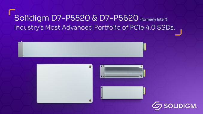
Diving right into matters, Solidigm is essentially picking up right where Intel left off, both in regards to product design and product naming. Intel was already seeing solid market penetration with its D-series branding, so there’s little reason to give up a good thing for the new Solidigm. In any case, the new drives are designed and marketed to slot right in as the next-generation parts in the D7 lineup, which is Solidigm’s highest performance drives for the enterprise and server market.
From a pure specification standpoint, the big news with the latest generation of drives is that Solidigm has doubled their capacities. The D7-P5620 will be available in capacities from 1.6TB to 12.8TB, while the D7-P5520 will go up to 15.36TB for its larger form factor drives. As you might expect, Solidigm is also using their own NAND here. The company's current tech is still their 144L TLC NAND, which means the P5620 has received a NAND upgrade (Intel never released a 144L P5600 series drive), while it's the same NAND as before for the P5520.
As with earlier iterations of the D7 family, both drives are built from the same platform – codename Arbordale Plus Refresh Refresh – meaning the same controller, NAND, and firmware. The only configuration difference between the drives is the amount of overprovisioning, with the P5600 drives using 20% overprovisioning to ensure faster performance, while the P5500 drives use just 4% overprovisioning to maximize capacity. Consequently, the P5620 is being pitched by the company as a mixed workload (mixed read/write) drive that can sustain up to 3 DWPD, while the P5520 is aimed at workloads with more reads than writes, with a 1 DWPD endurance.Solidigm D7 Enterprise SSDs D7-P5620 D7-P5600 D7-P5520 D7-P5510 Form Factor U.2 2.5" 15mm U.2 2.5" 15mm
E1.S 9.5mm/15mm
E1.L 9.5mmU.2 2.5" 15mm Interface PCIe 4.0 NVMe 1.4 PCIe 4.0 NVMe 1.3c PCIe 4.0 NVMe 1.4 PCIe 4.0 NVMe 1.3c Capacities 1.6TB
3.2TB
6.4TB
12.8TB1.6TB
3.2TB
6.4TB1.92TB
3.68TB
7.68TB
15.36TB (U.2 & E1L)3.68TB
7.68TBNAND Solidigm 144L TLC Intel 96L TLC Solidigm 144L TLC Intel 144L TLC Sequential Read 7100 MB/s 7000 MB/s 7100 MB/s 7000 MB/s Sequential Write 4200 MB/s 4300 MB/s 4200 MB/s 4200 MB/s Random Read (4 kB) 1.1M IOPS 1M IOPS 1.1M IOPS 930k IOPS Random Write (4 kB) 390k IOPS 260k IOPS 220k IOPS 190k IOPS Power Operating 20 W 18 W Idle 5 W 5 W Write Endurance 3 DWPD 3 DWPD 1 DWPD 1 DWPD Warranty 5 years
Update: Solidigm has sent over revised write IOPS figures for the P5620; their initial figures were a typo
Given the difference in overprovisioning, the two D7 drives carry different write performance ratings. While both drives are rated for 4.2GB/second for large sequential writes, the much larger spare area on the P5620 means it's rated to sustain 390K 4K write IOPS, which is a 50% improvement over its predecessor. Though it is interesting to note that the best performing SKU, according to Solidigm's specs, is not the highest capacity 12.8TB model, but rather the 6.4TB model, which is where the quoted figures come from. The 12.8TB model actually rated for slightly lower sustained write performance and write IOPS.
As for write performance on the P5520, that drive brings that down to 220K 4K write IOPS. Though even that is a 16% improvement over the P5510.
Meanwhile read speeds are up slightly across the board, with both drives topping out at 1.1M read IOPS, or 7.1GB/second sequential.
We don’t have any additional information from the company on the controller used, however based on the specifications, at this juncture there’s nothing to indicate it’s significantly different from the existing Arbordale Plus controller. Though it sounds like Solidigm may be tweaking things in firmware slightly differently than Intel did, as Solidigm is focusing on read latency (especially reads under write pressure) more than Intel. In the case of the P5500 series, they’ve knocked 4K read latency down from 84μs to 75μs for the P5520; meanwhile write latency has seen a smaller drop, saving off 1μs to bring it down to 15μs.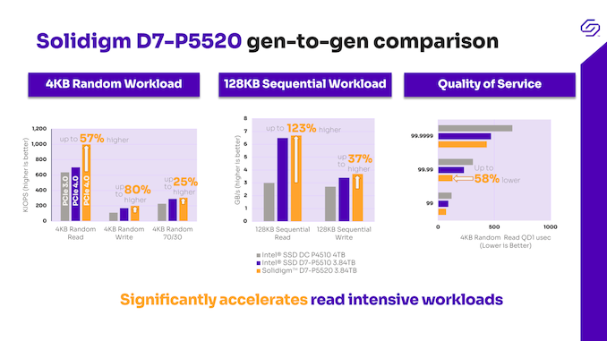
The launch of the P5520 also marks the significantly overdue introduction of EDSFF form factors for some of the D7 series drives. Along with the classic U.2 form factor that the drives have used for the last few generations, the P5520 will also be available in the E1.L and E1.S form factors. The latter is new territory for Solidigm, as even in the company’s lower-ender/higher-density D5 product lineup, they’ve only used E1.L previously. The P5520 E1.S drives, in turn, will actually come in two sizes: E1.S 9.5mm and E1.S 15mm. Both will offer the same reduced capacities – 7.68TB max versus double that for U2/E1.L – however the 15mm drive will use that space for a heatsink that the 9.5mm drive lacks the room to fit. Otherwise, the P5620 remains unchanged, and will only come in the U.2 form factor.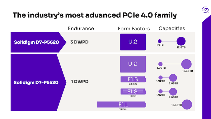
Wrapping things up, according to Solidigm the drives are already in mass production, and are even deployed with some OEMs and cloud providers.
Gallery: Solidgem D7-P5620/P5520 Press Deck


More...
-
04-26-22, 07:53 PM #11478
Anandtech: Kioxia Announces XG8 Client SSDs: PCIe 4.0 and BiCS5 For OEMs
Kioxia this morning is rolling out its next-generation of full-size client SSDs, the XG8 family. Like its predecessors, the XG8 is aimed at the OEM market, for customers who are after a full M.2 2280-sized drive and are looking for better performance than the company’s more integrated and compact BG-series drives. Notable features for the latest-generation drive include a PCIe 4.0-capable controller, as well as capacities as high as 4TB.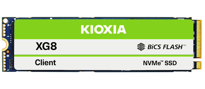
And while we’d normally use the company’s previous-generation drive as a baseline to illustrate what’s new with the latest drive, today’s announcement of the XG8 is a bit weird, even by Kioxia’s own OEM-centric standards. The predecessor to the XG8 is the XG7, which was launched in November of 2020 with a very similar feature set: a PCIe 4.0 M.2 2280 SSD with capacities up to 4TB. However, for reasons we’re still not entirely clear on, the XG7 only saw a very limited deployment among OEMs, to the point that Kioxia never even put together a proper product page for the part. As a result, the company is taking a mulligan of sorts and is starting fresh with the XG8, positioning it as the successor to the PCIe 3/BiCS4-based XG6.
Starting with the basics, the XG8 is a M.2 2280 form factor SSD with a PCIe 4.0 x4 connection. Kioxia is using their 5th generation, 112-layer BiCS5 NAND, with capacities ranging from 512GB up to 4TB. That NAND is being paired with their own in-house controller, which offers NVMe 1.4 support as well as the option for the usual OEM-centric security features such as TCG Pyrite 2.01 and TCG Opal 2.01.Kioxia XG8 SSD Specifications Capacity 512 GB 1 TB 2 TB 4 TB Form Factor M.2 2280 Interface PCIe Gen4 x4, NVMe 1.4 NAND Flash 112L BiCS5 3D TLC
Kioxia classifies the drive as a high-end product – particularly in relation to the BG5 – though as this is again by OEM standards, it’s a bit up in the air by enthusiast standards. Unfortunately, Kioxia isn’t providing any hard performance figures in advance of today’s announcement, so we don’t even have on-paper numbers to go by. For the moment, Kioxia is primarily throwing around 2x the performance of the XG6, most of which I’d expect to come from the switch to PCIe 4.0 and the additional host-to-controller bandwidth that affords.
Based on the lack of specification information and the fact that so many figures line up with the absentee XG7, it’s not at all clear what sets the XG8 apart from its more recent sibling. Presumably something has changed, if only to avoid another misfire, but at this point we’d just be guessing. Though it is notable that this drive family appears to be doing away with the ‘P’ designation that Kioxia used for high capacity drives in previous generations (e.g. XG6-P), as there is no mention of that sub-family of drives this time around.
Finally, this is probably one of the last BiCS5 client drives we’ll see from Kioxia. The WD/Kioxia joint venture has been producing BiCS5 NAND since late 2020, and according to recent WD earnings calls, 162L BiCS6 is expected to go into mass production late this year.
In the meantime, the XG8 is now sampling to Kioxia’s customers, and should start showing up in OEM laptops and desktops soon.
More...
-
04-28-22, 09:44 PM #11479
Anandtech: Intel Reports Q1 2022 Earnings: Improved Enterprise Sales Buoy Weaker Clie
Kicking off our coverage of the first earnings season of the year for the tech industry, we as always start with Intel. The blue-hued blue-chip company is the first out of the gate to report their results for the first quarter of 2022, with Intel reporting something of a mixed quarter. With revenue down on a yearly basis – thanks in large part to softer client sales – Intel is no longer on a hot streak of setting records. At the same time, however, the company has dialed back its lofty expectations accordingly, and as a result was still able to slightly edge out its Q1 guidance.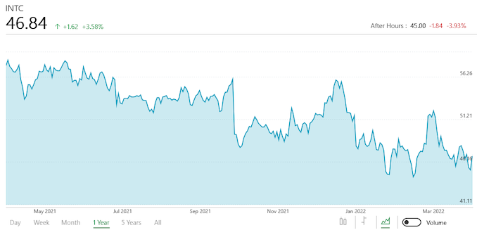
For the first quarter of 2022, Intel booked $18.4B in revenue, a drop of 7% from the year-ago quarter. Buffering the company against this revenue drop on a GAAP basis has been an improvement in both operating income and net income, both of which benefitted from some one-off restructuring and investment gains (McAfee equity sale). As a result, Intel booked $8.1B in net income on a GAAP basis, which is a 141% improvement on the year. Otherwise, stripping things back to non-GAAP financials, things more closely mirror the overall revenue picture with a 35% decline in income.
More...
-
04-29-22, 08:59 PM #11480
Anandtech: Intel: Meteor Lake Chiplet SoC Up and Running
Alongside Intel’s regular earnings report yesterday, the company also delivered a brief up on the state of one of their most important upcoming products, Meteor Lake. Intel’s first chiplet/tile-based SoC, which completed initial development last year, has now completed power-on testing and more. The news is not unexpected, but for Intel it still marks a notable milestone, and is important proof that both Meteor Lake and the Intel 4 process remain on track.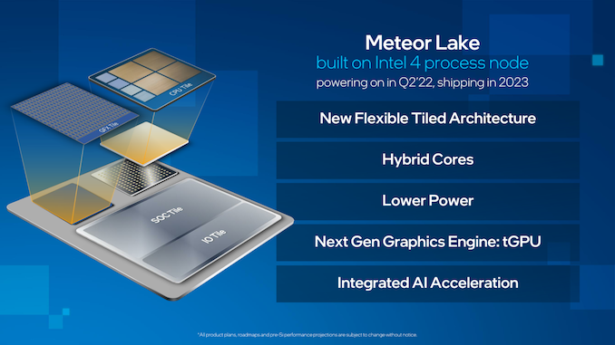
Meteor Lake, which is slated to be the basis of Intel’s 14th generation Core processors in 2023, is an important chip for the company on several levels. In terms of design, it is the first chiplet-based (or as Intel likes to put it, “disaggregated”) mass-market client SoC from the company. Intel’s roadmap for the Core lineup has the company using chiplet-style SoCs on a permanent basis going forward, so Meteor Lake is very important for Intel’s design and architecture teams as it’s going to be their first crack at client chiplets – and proof as to whether they can successfully pull it off.
Meanwhile Meteor Lake is also the first client part that will be built on the Intel 4 process, which was formerly known as Intel’s 7nm process. Intel 4 will mark Intel’s long-awaited (and delayed) transition to using EUV in patterning, making it one of the most significant changes to Intel’s fab technology since the company added FinFETs a decade ago. Given Intel’s fab troubles over the past few years, the company is understandably eager to show off any proof that its fab development cycle is back on track, and that they are going to make their previously declared manufacturing milestones.
As for this week’s power-on announcement, this is in-line with Intel’s earlier expectations. At the company’s 2022 investor meeting back in February, in the client roadmap presentation Intel indicated that they were aiming for a Q2’22 power-on.
We have officially powered-on our first disaggregated product: Meteor Lake. An incredible milestone resulting from the efforts of so many across @intel. Congratulations, team! pic.twitter.com/eKvHzDqSiuIn fact, it would seem that Intel has slightly exceeded their own goals. While in a tweet put out today by Michelle Johnston Holthaus, the recently named EVP and GM of Intel’s Client Computing Group, announced that Meteor Lake had been powered on, comments from CEO Pat Gelsinger indicate that Meteor Lake is doing even better than that. According to Gelsinger’s comments on yesterday’s earnings call, Meteor Lake has also been able to boot Windows, Chrome, and Linux. So while there remains many months of bring-up left to go, it would seem that Meteor Lake’s development is proceeding apace.
— Michelle Johnston Holthaus (@MJHolthaus) April 29, 2022
But that will be a story for 2023. Intel will first be getting Raptor Lake out the door later this year. The Alder Lake successor is being built on the same Intel 7 process as Alder Lake itself, and will feature an enhanced version of the Alder Lake architecture.
More...


 Quote
QuoteThread Information
Users Browsing this Thread
There are currently 19 users browsing this thread. (0 members and 19 guests)


Bookmarks