

Results 11,521 to 11,530 of 12091
Thread: Anandtech News
-
06-21-22, 11:02 AM #11521
Anandtech: Lenovo ThinkStation P360 Ultra Melds Desktop Alder Lake and NVIDIA Profess
Over the last decade or so, advancements in CPU and GPU architectures have combined extremely well with the relentless march of Moore's Law on the silicon front. Together, these have resulted in hand-held devices that have more computing power than huge and power-hungry machines from the turn of the century. On the desktop front, small form-factor (SFF) machines are now becoming a viable option for demanding professional use-cases. CAD, modeling, and simulation capabilities that required big iron servers or massive tower workstations just a few years back are now capable of being served by compact systems.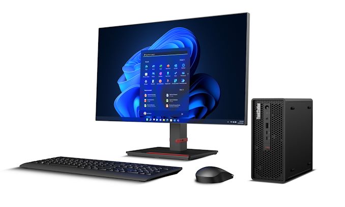
Workstation notebooks integrating top-end mobile CPUs and professional graphics solutions from AMD (FirePro) or NVIDIA (Quadro Mobile / RTX Professional) have been around since the mid-2000s. The advent of UCFF and SFF PCs has slowly brought these notebook platforms to the desktop. Zotac was one of the early players in this market, and continues to introduce new products in the Zotac ZBOX Q Series. The company has two distinct lines - one with a notebook CPU and a professional mobile GPU (with a 2.65L volume), and another with a workstation CPU (Xeons up to 80W) and a professional mobile GPU (with a 5.85L volume).
Today, Lenovo is also entering the SFF workstation PC market with its ThinkStation P360 Ultra models. The company already has tiny workstations that do not include support for discrete GPUs, and that is fixed in the new Ultra systems. Featuring desktop Alder Lake with an Intel W680 chipset (allowing for ECC RAM option), these systems also optionally support discrete graphics cards - up to NVIDIA RTX A5000 Mobile. Four SODIMM slots allow for up to 128GB of ECC or non-ECC DDR5-4000 memory. Two PCIe Gen 4 x4 M.2 slots and a SATA III port behind a 2.5" drive slot are also available, with RAID possibility for the M.2 SSDs. Depending on the choice of CPU and GPU, Lenovo plans to equip the system with one of three 89% efficiency external power adapters - 170W, 230W, or 300W.
The front panel has a USB 3.2 Gen 2 Type-A and two Thunderbolt 4 Type-C ports, as well as a combo audio jack. The vanilla iGPU version has four USB 3.2 Gen 2 Type-A ports, three DisplayPort 1.4 ports, and two RJ-45 LAN ports (1x 2.5 GbE, and 1x 1 GbE). On the WLAN front, the non-vPro option is the Wi-Fi 6 AX201, while the vPro one is the Wi-Fi 6E AX211. In addition to the PCIe 4.0 x16 expansion slot for the discrete GPU, the system also includes support for a PCIe 3.0 x4 card such as the Intel I350-T2 dual-port Gigabit Ethernet Adapter.
With dimensions of 87mm x 223mm x 202mm, the whole package comes in at 3.92L. In order to cram the functionality into such a chassis, Lenovo has employed a custom dual-sided motherboard with a unique cooling solution, as indicated in the teardown picture above. A blower fan is placed above the two M.2 slots to ensure that thte PCIe Gen 4 M.2 SSDs can operate without any thermal issues.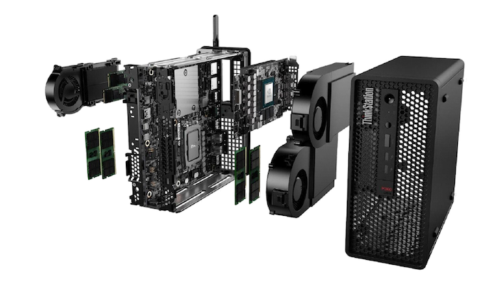
As is usual for Lenovo's business / professional-oriented PCs, these systems are tested to military grade requirements and come with ISV certifications fro companies such as Autodesk, ANSYS, Dassault, PTC, Siemens, etc. Pricing starts at $1299 for the base model without a discrete GPU.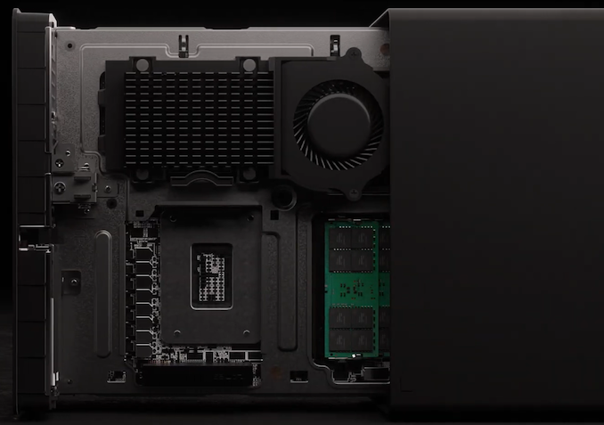
The ThinkStation P360 Ultra joins Lenovo's already-announced P360 Tiny and the P360 Tower models. The P360 Tiny doesn't support discrete GPUs, while the P360 Tower goes overboard with support for 3.5" drives, and up to four PCIe expansion cards, along with a 750W PSU. Most workstation use-cases can get by without all those bells and whistles. Additional options for the end consumer are always welcome, and that is where the P360 Ultra comes into play.
More...
-
06-22-22, 06:51 PM #11522
Anandtech: AMD Updates Ryzen Embedded Series, R2000 Series With up to Four Cores and
One area of AMD's portfolio that perhaps doesn't garner the same levels of attention as its desktop, mobile, and server products is its embedded business. In early 2020, AMD unveiled its Ryzen Embedded R1000 platform for the commercial and industrial sectors and the ever-growing IoT market, with low-powered processors designed for low-profile systems to satisfy the mid-range of the market.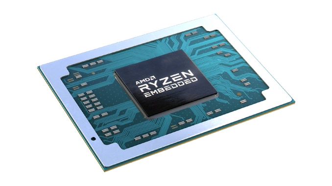
At Embedded World 2022 in Nuremberg, Germany, AMD has announced its next-generation of Ryzen Embedded SoCs, the R2000 series. Offering four different SKUs ranging from 2C/4T up to 4C/8T, which is double the core count of the previous generation, AMD claims that the R2000 series features up to 81% higher CPU and graphics performance.
The AMD Ryzen Embedded R2000 Series compared to the previous generation (R1000), now has double the core count, with a generational swing from Zen to the more efficient and higher performance Zen+ cores. All four SKUs announced feature a configurable TDP, with the top SKU, the R2544, operating at between 35 and 54 W. More in line with the lower power target of these SoCs, the bottom SKU (R2312) has a configurable TDP of between 12 and 35 W.
Another element delivering additional performance compared to the previous generation is better iGPU performance via increasing the number of Radeon Vega graphics compute units. The entry R2312 SKU comes with 3 CUs, while the R2544 comes with 8 CUs. The Ryzen Embedded R2000 series also benefits from newer video decode and display processor blocks, bringing support for decoding 4Kp60 video and driving up to three 4K displays.AMD Ryzen Embedded R2000-Series APUs AnandTech Core/
ThreadBase
Freq (MHz)1T Boost
Freq (MHz)Memory
SupportL2
CacheL3
CacheGPU
CU'sTDP
Range
(W)Launch
(Expected)R2544 4 8 3350 3700 DDR4-3200 2 MB 4 MB 8 35-54 October 22 R2514 4 8 2100 3700 DDR4-2667 2 MB 4 MB 8 12-35 October 22 R2314 4 4 2100 3500 DDR4-2667 2 MB 4 MB 6 12-35 In Production R2312 2 4 2700 3500 DDR4-2400 1 MB 2 MB 3 12-25 In Production
AMD has also equipped the SoCs with 16 PCIe Gen 3 lanes on the R2314, R2514, and R2544 SKUs, while the R2312 gets eight. The R2000 series has support for two SATA 3.0 ports, up to six USB ports with a mixture of USB 3.2 G2 and USB 2.0, and OS support for Microsoft Windows 11/10 and Linux Ubuntu LTS.
The application benefits of AMD's Ryzen Embedded R2000 series include the commercial and industrial sectors, as well as robotics, with a planned product availability of up to 10 years, ensuring a long life cycle for each product. Some of AMD's Ryzen Embedded R2000's Ecosystem partners include Advantech for its gaming and gambling machines, as well as DFI, IBASE, and Sapphire, so these new SoCs are already being adopted and planned into existing thin-client and small form factor systems.
AMD states that the Ryzen Embedded R2544 (4C/8T) and R2514 (4C/8T) will be available sometime in October 22, while the R2314 and R2312 SKUs are currently in production.
Source: AMD
More...
-
06-23-22, 07:50 AM #11523
Anandtech: The Gigabyte UD1000GM PG5 1000W PSU Review: Prelude to ATX 3.0
In today's review, we are taking a look at the first-ever PSU released with the new 12VHPWR connector, the GIGABYTE UD1000GM PG5. Although the unit is not ATX v3.0 compliant, GIGABYTE upgraded one of their currently available platforms to provide for a single 600W video card connector in an effort to entice early adopters.
More...
-
06-27-22, 04:36 PM #11524
Anandtech: As HPC Chip Sizes Grow, So Does the Need For 1kW+ Chip Cooling
One trend in the high performance computing (HPC) space that is becoming increasingly clear is that power consumption per chip and per rack unit is not going to stop with the limits of air cooling. As supercomputers and other high performance systems have already hit – and in some cases exceeded these limits – power requirements and power densities have continued to scale up. And based on the news from TSMC's recent annual technology symposium, we should expect to see this trend continue as TSMC lays the groundwork for even denser chip configurations.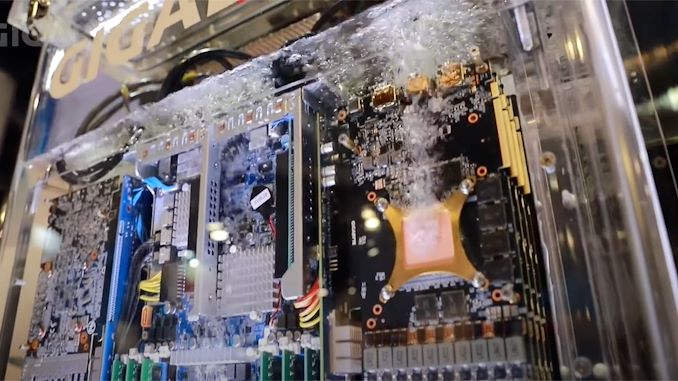
The problem at hand is not a new one: transistor power consumption isn't scaling down nearly as quickly as transistor sizes. And as chipmakers are not about to leave performance on the table (and fail to deliver semi-annual increases for their customers), in the HPC space power per transistor is quickly growing. As an additional wrinkle, chiplets are paving the way towards constructing chips with even more silicon than traditional reticle limits, which is good for performance and latency, but even more problematic for cooling.
Enabling this kind of silicon and power growth has been modern technologies like TSMC'a CoWoS and InFO, which allow chipmakers to build integrated multi-chiplet system-in-packages (SiPs) with as much a double the amount of silicon otherwise allowed by TSMC's reticle limits. By 2024, advancements of TSMC's CoWoS packaging technology will enable building even larger multi-chiplet SiP, with TSMC anticipating stitching together upwards of four reticle-sized chiplets, This will enable tremendous levels of complexity (over 300 billion transistor per SiP is a possibility that TSMC and its partners are looking at) and performance, but naturally at the cost of formidable power consumption and heat generation.
Already, flagship products like NVIDIA's H100 accelerator module require upwards of 700W of power for peak performance. So the prospect of multiple, GH100-sized chiplets on a single product is raising eyebrows – and power budgets. TSMC envisions that several years down the road there will be multi-chiplet SiPs with a power consumption of around 1000W or even higher, Creating a cooling challenge.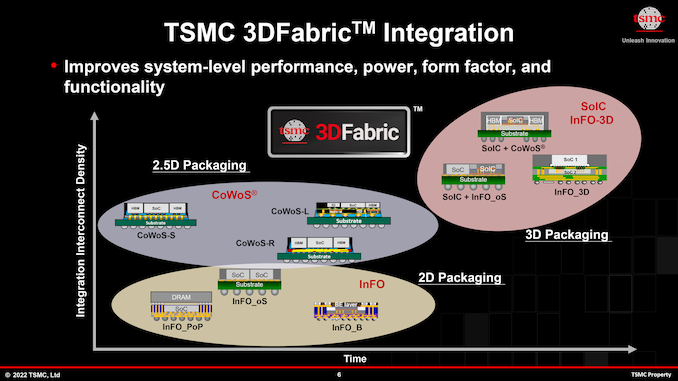
At 700W, H100 already requires liquid cooling; and the story is much the same for the chiplet based Ponte Vecchio from Intel, and AMD's Instinct MI250X. But even traditional liquid cooling has its limits. By the time chips reach a cumulative 1 kW, TSMC envisions that datacenters will need to use immersion liquid cooling systems for such extreme AI and HPC processors. Immersion liquid cooling, in turn, will require rearchitecting datacenters themselves, which will be a major change in design and a major challenge in continuity.
The short-tem challenges aside, once datacenters are setup for immersion liquid cooling, they will be ready for even hotter chips. Liquid immersion cooling has a lot of potential for handling large cooling loads, which is one reason why Intel is investing heavily in this technology in an attempt to make it more mainstream.
In addition to immersion liquid cooling, there is another technology that can be used to cool down ultra-hot chips — on-chip water cooling. Last year TSMC revealed that it had experimented with on-chip water cooling and said that even 2.6 kW SiPs could be cooled down using this technology. But of course, on-chip water cooling is an extremely expensive technology by itself, which will drive costs of those extreme AI and HPC solutions to unprecedented levels.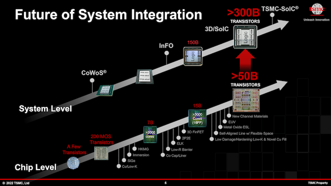
None the less, while the future isn't set in stone, seemingly it has been cast in silicon. TSMC's chipmaking clients have customers willing to pay a top dollar for those ultra-high-performance solutions (think operators of hyperscale cloud datacenters), even with the high costs and technical complexity that entails. Which to bring things back to where we started, is why TSMC has been developing CoWoS and InFO packaging processes on the first place – because there are customers ready and eager to break the reticle limit via chiplet technology. We're already seeing some of this today with products like Cerebras' massive Wafer Scale Engine processor, and via large chiplets, TSMC is preparing to make smaller (but still reticle-breaking) designs more accessible to their wider customer base.
Such extreme requirements for performance, packaging, and cooling not only push producers of semiconductors, servers, and cooling systems to their limits, but also require modifications of cloud datacenters. If indeed massive SiPs for AI and HPC workloads become widespread, cloud datacenters will be completely different in the coming years.
More...
-
06-29-22, 11:25 PM #11525
Anandtech: ASRock Releases Raptor Lake BIOS Updates For Its 600 Series Motherboards
While Intel has yet to officially announce its next (13th) generation of Core processors, this isn't stopping motherboard manufacturers from releasing products for them. Always eager to slide ahead of the competition and spur on new sales towards the later half of a platform's lifecycle, mobo makers are already releasing BIOSes that support Intel's future chips – parts which, officially speaking, don't even exist (yet).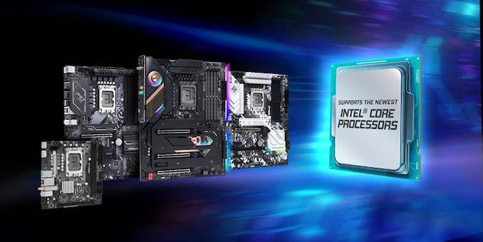
Leading this charge is ASRock, who today has released a wave of new BIOSes for its 600 series motherboards designed to support Intel's next generation of processors. Looking to the future, the wave of BIOS updates is the vast majority of its first-generation LGA1700 motherboards, including their Z690, H670, B660, and H610 models.
At present, Intel has not officially announced its Raptor Lake processors yet, which are set to be Intel's next-generation of processors for desktops. This is an interesting move from ASRock, which means users currently with an ASRock 600-series motherboard can update the firmware now and not have to worry about installing the 'next-gen' later on.
ASRock's EZ Update utility, alongside its models with BIOS Flashback, can install the update with a USB stick with the core file on it. However, it remains to be seen if pre-existing 600-series boards will be updated at the retail/distribution level before the launch of Raptor Lake.
The biggest question, though, is why right now? Intel hasn't gone as far as announcing its 13th Gen Core series yet, although it is expected to be sometime by the end of this year. Officially, Intel has kept things about the upcoming Raptor Lake processors under wraps, and there is still very little to go on outside of unconfirmed sources and 'leaks.'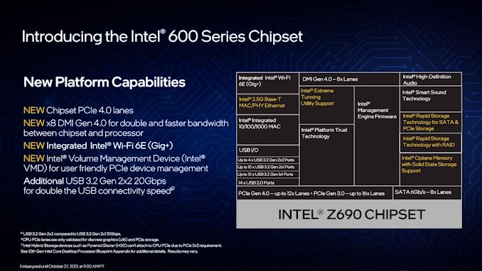
The current Intel Z690 chipset features and specifications
It's also worth noting that Intel is likely to announce a new motherboard chipset for its 13th Gen Core series processors, likely named Z790 following previous launches, which will also be on the LGA 1700 socket. This is much like with the release of the Z590 chipset, which also featured support for 11th and 10th Generation Core series processors.
Outside of ASRock's announcement, other motherboard vendors have been tight-lipped about the upcoming 13th Generation Core series processors and Intel. It remains to be seen if other vendors now choose to follow suit with ASRock in releasing firmware for unannounced processors, especially seeing as there are usually teething problems with launch day firmware, let alone firmware released months in advance.
Source: ASRock
More...
-
06-29-22, 11:25 PM #11526
Anandtech: TSMC: N2 To Start With Just GAAFETs, Add Backside Power Delivery Later
When TSMC initially introduced its N2 (2 nm class) process technology earlier this month, the company outlined how the new node would be built on the back of two new cutting-edge fab techniques: gate-all-around transistors, and backside power rails. But, as we've since learned from last week's EU symposium, TSMC's plans are a bit more nuanced than first announced. Unlike some of their rivals, TSMC will not be implementing both technologies in the initial version of their N2 node. Instead, the first iteration of N2 will only be implementing gate-all-around transistors, with backside power delivery to come with a later version of the node.
So far, TSMC has mentioned two distinctive features of N2: nano sheet gate-all-around (GAA) transistors, and backside power rails. GAA transistors have two unique advantages over FinFETs: they solve many challenges associated with the leakage current since GAAFET's channels are horizontal and are surrounded by gates around all four sides. Meanwhile, backside power rail enabled improved power delivery to transistors, which increases performance and lowers power consumption.
But, as it turns out, TSMC is not planning to start with both nanosheet GAA transistors and backside power rails in the initial generation of its N2 process technology. As disclosed by the company last week at their EU symposium, the first generation of N2 will only feature gate-all-around transistors. Backside power delivery, on the other hand, will come later with more advanced implementations of N2.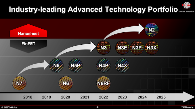
At this point the company hasn't said too much as to why they're not rolling out backside power delivery as part of their initial N2 node. But, in discussing the bifurcation, TSMC has noted that backside power delivery will ultimately add additional process steps, which the company is seemingly looking to avoid on their first try with GAAFETs.
The lack of backside power delivery in the original version of the N2 fabrication technology perhaps explains rather moderate performance improvement of N2 when compared to N3E node. While for high-performance computing (CPUs, accelerators, etc.) a 10% to 15% performance improvement at the same power and complexity does not seem to be impressive, a 25% to 30% power drop at the same speed and complexity seems to be very good for mobile applications.
*Chip density published by TSMC reflects 'mixed' chip density consisting of 50% logic, 30% SRAM, and 20% analog.Advertised PPA Improvements of New Process Technologies
Data announced during conference calls, events, press briefings and press releasesTSMC N5
vs
N7N3
vs
N5N3E
vs
N5N2
vs
N3EPower -30% -25-30% -34% -25-30% Performance +15% +10-15% +18% +10-15% Chip Density* ? ? ~1.3X >1.1X Volume
ManufacturingQ2 2022 H2 2022 Q2/Q3 2023 H2 2025
Considering that TSMC always offers multiple versions of its nodes, that TSMC has several variants planned for N2 is not all that surprising. Nonetheless, it is a bit odd to see that TSMC is taking a rather long road to backside power delivery.
Compared and contrasted to the competition, this will end up being a notable difference from how rival Intel is planning to handle their own GAAFET/backside power transition with the Intel 20A process. Intel intends to introduce its GAA RibbonFET transistors and PowerVia interconnects together in mid-2024 – going so far as to create an internal pseudo node just to focus on RibbonFET development. TSMC, on the other hand, is taking a more cautious approach to risks and innovations, one which potentially has TSMC moving at a slower pace, but is also an approach that has traditionally been a better fit for TSMC's need to deliver more constant and consistent updates to its fab offerings.
And while we're still a few years out, it will be interesting to see what this means for the competitiveness of TSMC's first-generation N2 node. Will a GAAFET process without backside power delivery be at a meaningful disadvantage? Per current schedules, we'll find out the answer to that in the second half of 2025, when TSMC's first N2 node is slated to enter high-volume manufacturing (HVM).
More...
-
06-30-22, 01:42 PM #11527
Anandtech: The AMD Ryzen 7 5800X3D Review: 96 MB of L3 3D V-Cache Designed For Gamers
The level of competition in the desktop CPU market has rarely been as intensive as it has been over the last couple of years. When AMD brought its Ryzen processors to market, it forced Intel to reply, and both have consistently battled in multiple areas, including core count, IPC performance, frequency, and ultimate performance. The constant race to improve products, stay ahead of the competition, and meet customers' changing needs has also sent the two companies off of the beaten paths at times, developing even wilder technologies in search of that competitive edge.
In the case of AMD, one such development effort has culminated with 3D V-Cache packaging technology, which stacks a layer of L3 cache on top of the existing CCD's L3 cache. Owing to the fact that while additional cache is beneficial to performance, large quantities of SRAM are, well, large, AMD has been working on how to place more L3 cache on a CPU chiplet without blowing out the die size altogether. The end result of that has been the stacked V-Cache technology, which allows the additional cache to be separately fabbed and then carefully placed on top of a chip to be used as part of a processor.
For the consumer market, AMD's first V-Cache equipped product is the Ryzen 7 5800X3D. Pitched as the fastest gaming processor on the market today, AMD's unique chip offers eight cores/sixteen threads of processing power, and a whopping 96 MB of L3 cache onboard. Essentially building on top of the already established Ryzen 7 5800X processor, the aim from AMD is that the additional L3 cache on the 5800X3D will take gaming performance to the next level – all for around $100 more than the 5800X.
With AMD's new gaming chip in hand, we've put the Ryzen 7 5800X3D through CPU suite and gaming tests to see if it is as good as AMD claims it is.
More...
-
06-30-22, 01:42 PM #11528
Anandtech: Samsung Starts 3nm Production: The Gate-All-Around (GAAFET) Era Begins
Capping off a multi-year development process, Samsung’s foundry group sends word this morning that the company has officially kicked off production on its initial 3nm chip production line. Samsung’s 3nm process is the industry’s first commercial production process node using gate-all-around transistor (GAAFET) technology, marking a major milestone for the field of silicon lithography, and potentially giving Samsung a major boost in its efforts to compete with TSMC.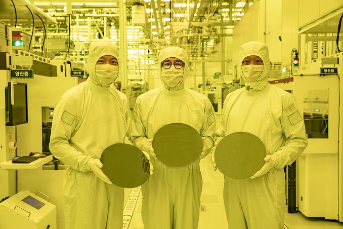
The relatively spartan announcement from Samsung, which comes on the final day of Q2, announces that Samsung has begun production of chips on a GAAFET-enabled 3nm production line. The company is not disclosing the specific version of the node used here, but based on previous Samsung roadmaps, this is undoubtedly Samsung’s initial 3GAE process – essentially, Samsung’s earliest process node within a family. According to Samsung, the line will initially be used to produce chips for “high performance, low power computing”, with mobile processors to come later. Samsung’s early process nodes are traditionally reserved for the company’s internal use, so while Samsung isn’t announcing any specific 3nm chips today, it’s only a matter of time until we see a 3nm SoC announces from Samsung LSI.
Samsung has, for the most part, been quiet about its progress on 3nm/GAAFET this year. The last significant news we heard from the company on the matter was several months ago at the company’s Foundry Forum event, where the company reiterated plans to get 3GAE into production by the end of 2022. Given the previous silence and the cutting-edge nature of the technology, there had been more than some concern that 3GAE would be delayed past 2022 – adding on to delays that pushed the tech out of its original 2021 launch window – but with today’s announcement Samsung seems to want to put that to rest.
With that said, the devil is in the detail in these announcements, especially as to what’s said versus not said. Taken literally, today’s announcement from Samsung notably does not include any mention of “high volume” manufacturing, which is the traditional milestone for when a process node is ready for commercial use. So by merely saying 3nm is in production, Samsung’s announcement leaves the company with a fair bit of wiggle room with regards to just how many chips they’re capable of producing – and at what yields. The company was producing test chips back in 2021, so the matter is more nuanced than just firing up the fab, so the line between PR and productization is fuzzy, to say the least.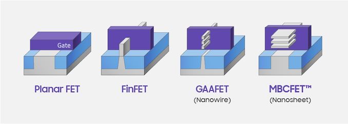
Still, today’s announcement is a major moment for Samsung, who has been working on 3nm/GAAFET technology since before 2019, when they initially announced the technology. Samsung’s specific flavor of GAA transistor technology is Multi Bridge Channel FET (MBCFET), which is a nanosheet-based implementation. Nanosheet-based FETs are extremely customizable, and the width of the nanosheet is a key metric in defining the power and performance characteristics: the higher the width, the higher the performance (at higher power). As a result, transistor designs that focus on low power can use smaller nanosheets, while logic that requires higher performance can go for the wider sheets.
Along with today’s production announcement, Samsung has also offered some updated size and performance figures comparing 3GAE to older nodes. Officially, 3GAE can offer 45% reduced power consumption or 23% improved performance compared to Samsung’s 5nm process (the company doesn’t state which flavor), with an overall reduction in feature size of 16%. These figures are notably different from Samsung’s previous (2019) figures, which compared the tech to Samsung’s 7LPP node. Given the change in baselines, it’s not clear at this point whether 3GAE is living up to Samsung’s initial claims, or if they’ve had to back off a bit for the initial version of their 3nm technology.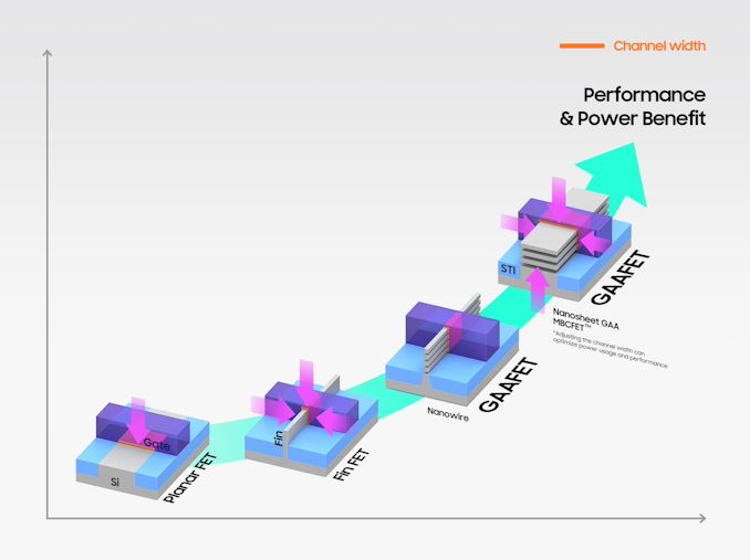
What is clear, however, is that Samsung has more significant improvements in mind for the second iteration of 3nm, which we know is 3GAP(lus). According to today’s press release, Samsung is expecting a 50% power reduction or 30% performance improvement versus the same 5nm baseline, with a much greater 35% area reduction. Today’s announcement doesn’t offer a date for 3GAP, but per previous roadmaps, 3GAP is expected to land around a year after 3GAE. 3GAP is also when we expect to see Samsung open the door to outside customers, though given the harsh competitive environment, nothing should be taken for granted.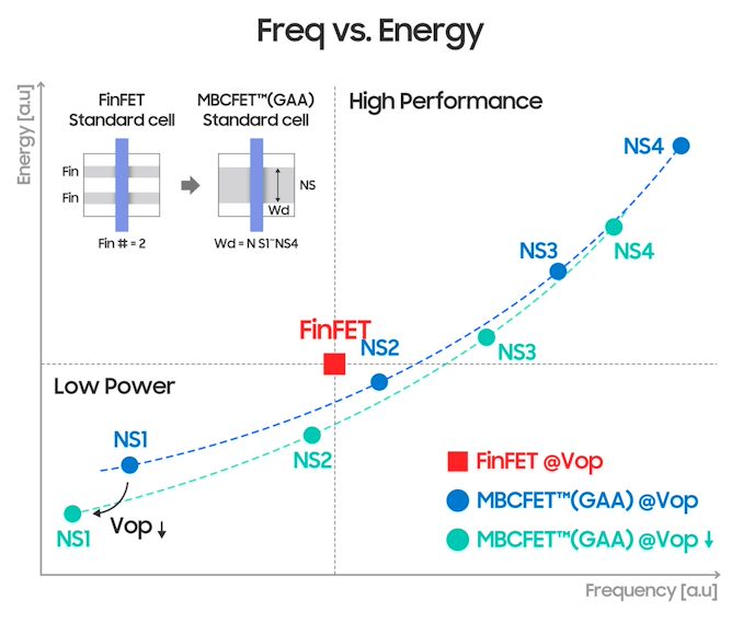
The launch of Samsung’s 3nm process tech comes as the company is working to regain its footing against arch rival TSMC, who has clearly pulled into the lead in the 5nm/4nm generation. The gap between TSMC and Samsung has been wide enough that major customers such as Qualcomm have been porting high-performance chips like the Snapdragon 8 series from Samsung to TSMC, and at this point Samsung has seen few major 5nm/4nm wins compared to TSMC. If everything goes well, being the first fab with GAAFET tech could give Samsung a temporary-but-material advantage over TSMC, whose 3nm process is still using older FinFET-style transistors. But in order to pull that off, Samsung will need to reverse their earlier technical problems and deliver a performant, high-yielding process that’s far enough ahead to woo skeptical customers.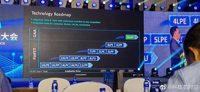
Samsung Process Roadmap (July 2021)
Gallery: Samsung Starts 3nm GAAFET Production


More...
-
07-05-22, 07:19 AM #11529
Anandtech: The AmazonBasics Aurora Vista 1500 UPS Review: Passable Power
AmazonBasics is a private label of products owned by Amazon. The subsidiary was founded back in 2009 and initially offered only basic products, such as cables and office consumables. More and more products are being added under the AmazonBasics label every day. Today, Amazon retails thousands of products under the AmazonBasics label, ranging from paperclips to living room sets. The only common point amongst all of these products is that they are very aggressively priced, usually selling for significantly less than any other competitive product from an established brand.
In this review, we are having a look at a very popular low-cost UPS that Amazon distributes under the AmazonBasics label, the AmazonBasics Aurora Vista 1500VA. Much like its name suggests, it is a very basic design with minimal features, yet it is very aggressively priced. Taking the renowned Amazon customer service into account, it seems like an amazing deal for that kind of output.
More...
-
07-06-22, 10:50 AM #11530
Anandtech: Samsung MUF-256DA USB-C Flash Drive Review: Thumb-Sized Performance Consis
Portable SSDs have seen great demand over the last few years. Advancements in flash technology and controllers has resulted in compact drives delivering blistering speeds. These advancements have also had their effects on the ubiquitous thumb drives. Samsung's MUF-256DA is a compact USB Type-C flash drive available in capacities ranging from 64GB to 256GB. Today's review attempts to figure out how this USB flash drive (UFD) with a native flash controller stacks up against other native controller offerings in the market.
More...


 Quote
QuoteThread Information
Users Browsing this Thread
There are currently 19 users browsing this thread. (0 members and 19 guests)


Bookmarks