

Results 11,581 to 11,590 of 12089
Thread: Anandtech News
-
10-06-22, 09:09 PM #11581
Anandtech: AMD Issues Early Q322 Financial Results: Misses Guidance By $1B as Client
Underscoring a difficult second half of the year that seems to be shaping up for the entire tech industry, AMD this afternoon has become the latest tech company to warn investors that revenues for the quarter are going to come in significantly under previous guidance. Releasing a preliminary third quarter financial results statement, AMD is reporting that revenues for the quarter will come in at around $5.6 billion, which is over $1 billion below AMD’s previous guidance of $6.7 billion. Driving this unexpected drop in revenues is an exceptionally weak client market, with revenues down 40% versus Q3’21 and resulting in what’s traditionally AMD’s largest market segment by revenue becoming their smallest.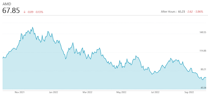
More...
-
10-10-22, 11:29 AM #11582
Anandtech: Samsung Foundry Outlines Roadmap Through 2027: 1.4 nm Node, 3x More Capaci
Samsung outlined its foundry business roadmap for the next five years at its Foundry Forum event last week. The company plans to introduce its next generation fabrication technologies in a timely manner and intends to make chips on its 1.4 nm (14 angstroms) manufacturing process by 2027. Also, the company will keep investing in new manufacturing capacity going forward as it strives to strengthen its position in the foundry market.
New Nodes Incoming
Samsung has been introducing new production nodes and/or variants on production nodes every 12 – 18 months for several years now, and plans to keep its rather aggressive pace going forward. Though the company’s roadmap illustrates, fanfare aside, that it is now taking longer to develop new fabrication processes. The company’s second-generation 3 nm-class gate-all-around (3GAP) technology is now set to arrive sometime in 2024. Meanwhile, Samsung Foundry intends to be ready with its 2 nm (20 angstroms) node in 2025, and with its 1.4 nm-branded fabrication process in 2027.
"With the company's success of bringing the latest [3 nm-class] process technology to mass production, Samsung will be further enhancing gate-all-around (GAA) based technology and plans to introduce the 2 nm process in 2025 and 1.4 nm process in 2027," a statement by Samsung reads.
Painting some very broad strokes, compared to those of Intel and TSMC, it seems like TSMC is a little bit more conservative (which is something expected when you are the world's largest contrast maker of microelectronics). Whereas Intel is more aggressive (which is again expected given the company's position in the market of semiconductors). Meanwhile, naming of fabrication processes these days is essentially aspiratory, with little connection to their real physical measures. Which is why comparing different semiconductor companies' roadmaps is an imprecise metric at best.Chip Fab Roadmaps
Data announced during conference calls, events, press briefings and press releasesHVM Start 2023 2024 2025 2026 2027 Intel Process Intel 3 Intel 20A Intel 18A ? ? FET FinFET RibbonFET + PowerVia ? ? EUV 0.33 NA EUV 0.55 High-NA EUV Samsung Process 3GAE 3GAP 2.0 nm 1.4 nm FET GAAFET ? ? ? EUV 0.33 NA EUV ? ? ? TSMC Process N3E/N3P N3S/N3X N2 N2? FET FinFET GAAFET GAAFET with backside power delivery (?) EUV 0.33 NA EUV ? ? ?
In addition to new 'general' nodes, Samsung plans to expand its process technology optimization programs for each specific application as well as customized services for customers, the company said.
Meanwhile, one of the things that Samsung notably did not mention in its press release concerning its 1.4 nm node is usage of High-NA equipment. Intel, for its part, plans to use High-NA starting its Intel 18A node (in 2024), where it will eventually be supplanting the EUV multi-patterning used on initial 18A production.
According to Samsung, the adoption of new process technologies and demand for new fabrication processes will be driven by already known mega trends — AI, autonomous vehicles, automotive applications in general, HPC, 5G, and eventual 6G connectivity. Keeping in mind that Samsung is a large industrial conglomorate with many divisions, many of applications that it intends to address with future process nodes are its own.
The company disclosed last week that its LSI Business (chip development division) currently offers around 900 products, which include SoCs, image sensors, modems, display driver IC (DDI), power management IC (PMIC), and security solutions. Going forward the company plans to put even more efforts into development of performance-demanding IP, including CPU and GPU, by working closer with its industry partners (which presumably includes Arm and AMD).
Expanded Production Capacity
Offering state-of-the-art production technologies is good, but to produce those advanced chips in sufficient quantities to meet market demands is equally important. To that end, Samsung announced that the company will also continue to invest heavily into building out additional production capacity. In the recent years Samsung's semiconductor capacity CapEx was around $30 billion a year and it does not look like the firm plans to put a cap on its spendings (though it is noteworthy that it does not disclose how much money it intends to spend).
Samsung plans to expand its production capacity for its 'advanced' process technologies by more than three-fold by 2027. While the companies is not naming the nodes it considers "advanced", we would expect a significant addition of its EUV capacity in the next five years – especially as more ASML EUV machines become available. Meanwhile, the company will adopt 'Shell-First' tactics in its expansion and construct buildings and clean rooms first, and add equipment later on depending on market conditions.
Samsung's new fab under construction near Taylor, Texas, will be one of the company's main vehicles to add capacity in the coming years. The shell-first site will start to produce chips in 2024. And as the company adds new tools to the fab and build new phases, production capacity of the site will further increase.
Source: Samsung
More...
-
10-10-22, 11:28 PM #11583
Anandtech: Micron Announces 20-Year Plan To Build $100 Billion U.S. Fab Complex
Now that the U.S. government has finally settled the matter of whether it would be providing subsidies to entice chip fabs to setup shop within the U.S., those fabs and chip makers are starting to hammer out their domestic investment plans. Of all of the proposals revealed so far, Micron's new proposal stands to be the most ambitious. Last week the company announced plans to build the largest chip production complex in the history of the U.S. in central New York state. The plan will span 20 years of construction and upgrades, with a total price tag expected to hit around $100 billion by the time Micron is finished in the 2040s.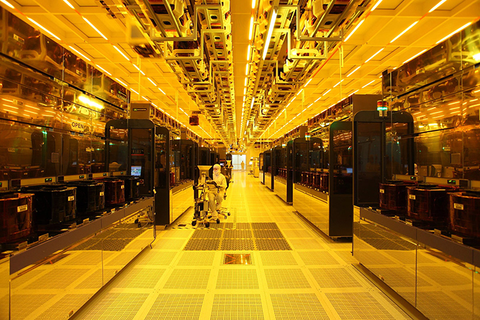
Micron's new site near Clay, New York, will not only be the company's largest campus ever built, but will also be the largest chip fab in the USA. The new Micron campus will produce DRAM using leading-edge process technologies and is expected to eventually include four 600,000 feet2 (55,700 meters2) clean rooms. Which, to provide some context, is roughly eight-times the clean room space of GlobalFoundries' Fab 8. The new fab complex will complement Micron's already announced campus near Boise, Idaho, that is expected to start coming online starting in 2025. Both sites will be instrumental to meet Micron's goal to produce 40% of its DRAM in the U.S. over the next decade.
According to Micron, the company's investments in its New York production facility will total $100 billion when fully built, and it will create some 9,000 Micron jobs along with some 41,000 indirect jobs. The first phase of the Clay, New York, project is expected to cost Micron around $20 billion in total over the rest of this decade. The DRAM maker expects to get $5.5 billion in incentives from the state of New York over the life of the project, as well as federal grants and tax credits from the CHIPS and Science Act. In addition, Micron and the state of New York will also invest $500 million over the next 20+ years in community and workforce development.
Micron plans to start site preparation work in 2023 and start construction in 2024. The facility ramp up is set to begin in the second half of the decade based on industry demand for DRAM devices.
Broadly speaking, fab complexes with eye-popping price tags are quickly becoming the norm in the fab industry as the cost of building and equipping successive generations of fabs continues to balloon. And while Micron is not the first company to plan for a twelve digit price tag for a new fab complex (Intel's new fab complex in Ohio is officially expected to cost around $100 billion when completed), Micron's announcement is notable in that unlike Intel and TSMC, Micron isn't a logic producer. So the company's $100 billion plans are entirely for memory, a relatively bold commitment for a conservative company that's competing in the tech industry's classic commodity market.
Bearing in mind that the new fab in in Onondaga County, New York, is not set to come online until the later half of the decade, it is too early for Micro to reveal which process technologies and types of products it will produce. The only thing that the company says is that this will be a leading-edge facility that will produce advanced DRAM products (think 64Gb DDR5 chips, DDR6 DRAMs, next-generation HBM, etc.) using EUV-enabled production nodes.
"Micron will leverage the diverse, highly educated and skilled talent in New York as we look to build our workforce in the Empire State," said Sanjay Mehrotra, chief executive of Micron. "This historic leading-edge memory megafab in Central New York will deliver benefits beyond the semiconductor industry by strengthening U.S. technology leadership as well as economic and national security, driving American innovation and competitiveness for decades to come."
Source: Micron
More...
-
10-13-22, 07:10 AM #11584
Anandtech: The Iceberg Thermal IceSLEET G6 Stealth Review: Top-Tier Colossal Tower Co
In today's review, we are taking a look at the flagship product of Iceberg Thermal, a relatively new US-based company. The IceSLEET G6 Stealth cooler that we are putting to the test today is a behemoth of a CPU cooler, intended to bring quiet cooling to users who want the very best but without the added complexity of liquid-based coolers.
More...
-
10-14-22, 04:37 PM #11585
Anandtech: NVIDIA Scrubs GeForce RTX 4080 12GB Launch; 16GB To Be Sole RTX 4080 Card
In a short post published on NVIDIA’s website today, the company has announced that it is “unlaunching” their planned GeForce RTX 4080 12GB card. The lowest-end of the initially announce RTX 40 series cards, the RTX 4080 12GB had attracted significant criticism since it’s announcement for bifurcating the 4080 tier between two cards that didn’t even share a common GPU. Seemingly bowing to the pressure of those complaints, NVIDIA has removed the card from their RTX 40 series lineup, as well as cancelling its November launch.
NVIDIA’s brief message reads as follows:
The RTX 4080 12GB is a fantastic graphics card, but it’s not named right. Having two GPUs with the 4080 designation is confusing.NVIDIA is not providing any further details about their future plans for the AD104-based video card at this time. However given the circumstances, it’s a reasonable assumption right now that NVIDIA now intends to launch it at a later time, with a different part number.
So, we’re pressing the “unlaunch” button on the 4080 12GB. The RTX 4080 16GB is amazing and on track to delight gamers everywhere on November 16th.
If the lines around the block and enthusiasm for the 4090 is any indication, the reception for the 4080 will be awesome.
Taking a look at the specifications of the cards, it’s easy to see why NVIDIA’s core base of enthusiast gamers were not amused. While both RTX 4080 parts shared a common architecture, they did not share a common GPU. Or, for that matter, common performance.NVIDIA GeForce Specification Comparison RTX 4090 RTX 4080 16GB RTX 4080 12GB
(Cancelled)CUDA Cores 16384 9728 7680 ROPs 176 112 80 Boost Clock 2520MHz 2505MHz 2610MHz Memory Clock 21Gbps GDDR6X 22.4Gbps GDDR6X 21Gbps GDDR6X Memory Bus Width 384-bit 256-bit 192-bit VRAM 24GB 16GB 12GB Single Precision Perf. 82.6 TFLOPS 48.7 TFLOPS 40.1 TFLOPS Tensor Perf. (FP16) 330 TFLOPS 195 TFLOPS 160 TFLOPS Tensor Perf. (FP8) 660 TFLOPS 390 TFLOPS 321 TFLOPS TDP 450W 320W 285W L2 Cache 72MB 64MB 48MB GPU AD102 AD103 AD104 Transistor Count 76.3B 45.9B 35.8B Architecture Ada Lovelace Ada Lovelace Ada Lovelace Manufacturing Process TSMC 4N TSMC 4N TSMC 4N Launch Date 10/12/2022 11/16/2022 Never Launch Price MSRP: $1599 MSRP: $1199 Was: $899
The RTX 4080 12GB, as it was, would have been based on the smaller AD104 GPU, rather than the AD103 GPU used for the 16GB model. In practice, this would have caused the 12GB model to deliver only about 82% of the former’s shader/tensor throughput, and just 70% of the memory bandwidth. A sizable performance gap that NVIDIA’s own figures ahead of the launch have all but confirmed.
NVIDIA, for its part, is no stranger to overloading a product line in this fashion, with similarly-named parts delivering unequal performance and the difference denoted solely by their VRAM capacity. This was a practice that started with the GTX 1060 series, and continued with the RTX 3080 series. However, the performance gap between the RTX 4080 parts was far larger than anything NVIDIA has previously done, bringing a good deal more attention to the problems that come from having such disparate parts sharing a common product name.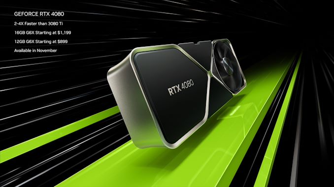
Of equal criticism has been NVIDIA’s decision to sell an AD104 part as an RTX 4080 card to begin with. Traditionally in NVIDIA’s product stack, the next card below the xx80 card is some form of xx70 card. And while video card names and GPU identifiers are essentially arbitrary, NVIDIA’s early performance figures painted a picture of a card that would have performed a lot like the kind of card most people would expect from the RTX 4070 – delivering performance upwards of 20% (or more) behind the better RTX 4080, and on-par with the last-generation flagship, the RTX 3090 Ti. In other words, there has been a great deal of suspicion within the enthusiast community that NVIDIA was attempting to sell what otherwise would have been the RTX 4070 as an RTX 4080, while carrying a higher price to match.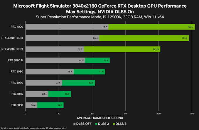
In any case, those plans are now officially scuttled. Whatever NVIDIA has planned for their AD104-based RTX 40 series card is something only the company knows at this time. Meanwhile come November 16th when the RTX 4080 series launches, the 16GB AD103-based cards will be the only offerings available, with prices starting at $1199.
More...
-
10-14-22, 04:37 PM #11586
Anandtech: Microsoft: DirectStorage 1.1 with GPU Decompression Finally on Its Way
As part of this week’s Microsoft Ignite developers conference, Microsoft’s DirectX team has published a few blog posts offering updates on the state of various game development-related projects. The biggest and most interesting of these is an update on DirectStorage, Microsoft’s API for enabling faster game asset loading. In short, the long-awaited 1.1 update, which adds support for GPU asset decompression, is finally on its way, with Microsoft intending to release the API to developers by the end of this year.
More...
-
10-19-22, 12:22 PM #11587
Anandtech: Intel Builds On USB4 v2 for 120 Gbps Next Generation Thunderbolt
The DisplayPort 2.1 specifications were officially released by VESA on Monday, and this was followed up by USB-IF's announcement of the release of the 80 Gbps USB4 v2 specifications yesterday. These have have brought to fore the significant engineering efforts put into creating a unified protocol capable of handling the external I/O bandwidth requirements of tomorrow's computing systems. Today, Intel is announcing the demonstration of early prototypes for next-generation Thunderbolt based on the USB4 v2 and DisplayPort 2.1 specifications.
Intel's donation of the Thunderbolt 3 specifications to the USB promoters group to form the basis of USB4 has had its share of pros and cons. On one hand, the convergence of the Type-C connector ecosystem theoretically achieved the goal of minimizing end-user confusion, and the royalty-free spec for PCIe tunneling opened up the market to other silicon vendors like ASMedia. However, it also created consumer angst as most of the attractive features of USB4 (such as the 40Gbps bandwidth and compatibility with PCIe tunneling) were entirely optional features. That said, it did enable Intel to market Thunderbolt ports as the Type-C that could do it all. Intel's demonstration of Next Generation Thunderbolt also included a sneak peek into its specifications, even though certain aspects are yet to be finalized. Before delving deeper into Intel's press release, a quick recap of the 80 Gbps USB4 v2 specifications announcement is necessary.
USB4 v2 Updates
USB4 v2 builds upon the multi-protocol tunneling architecture introduced in USB4 by doubling the available bandwidth while maintaining the same port / pins layout and cable structure. This has been achieved by moving the physical layer signal encoding to PAM3 (described in detail in our coverage of 80 Gbps 'Thunderbolt 5' last year). This means that existing 40Gbps USB4 cables will be able to support 80Gbps operation also.
The USB4 v2 specifications now allow tunneling of DisplayPort 2.1 signals and up to four PCIe 4.0 lanes. The data and display protocol updates also make it more efficient, with USB data tunneling capable of exceeding 20 Gbps.
One of the key updates in the move to support DisplayPort 2.1 tunneling relates to the maximum total bandwidth for four lanes in UHBR 20 transmission mode. This translates to 80 Gbps, essentially leaving nothing spare on the transmit side for any other protocol. To handle this, USB4 v2 introduces the concept of asymmetric links. In general, a USB4 link uses two bonded high-speed differential signaling pairs to transmit and receive data, allowing for 40 Gbps duplex operation (40 Gbps transmit and 40 Gbps receive) in the symmetric case. However, the lane initialization process can optionally configure the link to have 3 transmitters and one receiver on one side, and 3 receivers and one transmitter on the other. Combined with the higher data rates thanks to PAM3, this can allow the host to send out 120 Gbps, while lowering the receive bandwidth to 40 Gbps. High-resolution displays can be reliably driven without too much of a sacrifice of the bandwidth available on the transmit side for other purposes (like high-speed storage).
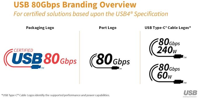
The power delivery specifications have also been updated to match the updates made in USB4 v2, and new logo guidelines have been issued for consumer-facing equipment.
Next-Generation Thunderbolt
Thunderbolt has seen incredible momentum over the last couple of years - triggered mainly by the integration of Thunderbolt controllers inside the high-volume notebook processors starting with Ice Lake. The combination of data, video, and power delivery in one port / cable makes it beneficial to a host of use-cases. In particular, the increasing popularity of hybrid work / hot-desking (monitors / networking etc. behind a dock, allowing multiple employees to just plug in their Thunderbolt-equipped systems at different times) has also served as a fillip to Thunderbolt adoption in the business / office space. Gamers and content creators have an incredible thirst for I/O bandwidth that is served well by Thunderbolt.
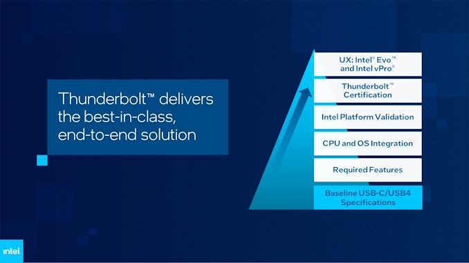
As mentioned earlier, Next Generation Thunderbolt takes the USB4 v2 specifications as baseline and makes all of the attractive optional features into mandatory ones. On top of this, Intel's integration of Thunderbolt into the notebook processors ensures that the implementation is power efficient on the host side. Making Thunderbolt mandatory for Intel Evo and vPro notebooks further cements Intel's leadership in the USB4 v2 space.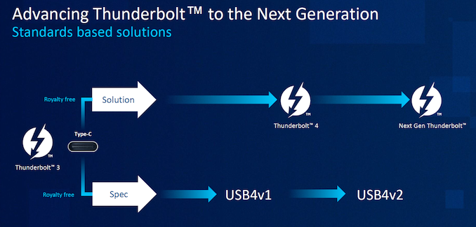
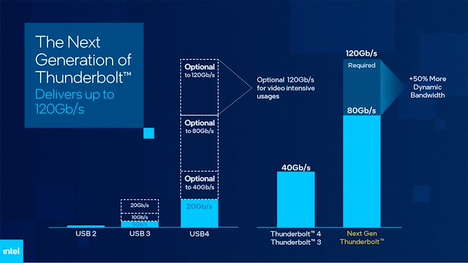

The dynamic bandwidth rebalancing feature allowing tunneling of the highest bandwidth DisplayPort 2.1 streams while still allowing usage of high-bandwidth peripherals is one of the most exciting features of USB4 v2 that is sure to be available in systems equipped with the Next Generation Thunderbolt ports.
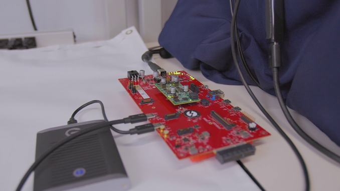
Intel's demonstration included both host and device implementations, with the host configuration shown in the beginning. A discrete GPU's DisplayPort output is fed into the host controller board, and two Type-C cables fork off, one ostensibly to the display, and another to a dock (device) with a SSD attached.
Aspects such as power delivery limits (Thunderbolt 3 / 4 support up to 15W by default) for the Next-Generation Thunderbolt ports will be clarified in the near future. Intel did not provide any information related to market availability.
Based on a glance through the USB4 v2 specifications and Intel's description of Next-Generation Thunderbolt, it is clear that Thunderbolt ports will continue to remain the Type-C port that does it all.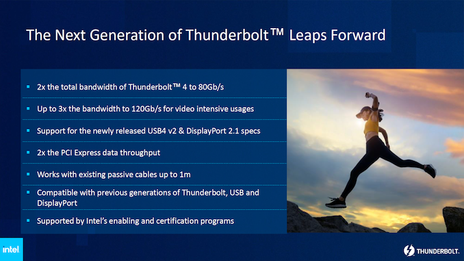
More...
-
10-20-22, 09:50 AM #11588
Anandtech: Intel Core i9-13900K and i5-13600K Review: Raptor Lake Brings More Bite
Today marks the release of Intel’s 13th Gen Core series, codenamed Raptor Lake. The first models to be unleashed into retail channels are all overclockable parts, with six SKUs across the Core i9, i7, and i5 product segments. While we’ve seen Intel’s heterogeneous or hybrid design with the launch of Intel’s Alder Lake (12th Gen Core) products, the latest Raptor Lake core brings a very similar design to the table, but with subtle improvements designed to help give Intel the leading edge in the desktop market.
First of these is a ‘new’ Raptor Cove performance (P) core using a refined Intel 7 manufacturing process with some subtle yet critical improvements to the LGA1700 platform to help increase generational performance. Perhaps the most significant benefit comes from adding more efficiency (E) cores, with the flagship SKU, the Core i9-13900K, bringing a total of 24-cores (8P+16E). Which means Intel has effectively doubled the number of efficiency cores on the die.
While there are plenty of talking points, ultimately, the proof, or in this case, performance, is in the pudding. With AMD pulling the trigger on its new Zen 4 core built on TSMC’s 5 nm process, does Intel’s 13th generation Core processors have what it takes to go toe-to-toe with the impressive Ryzen 7000? We aim to discover how Raptor Lake shapes up in our review of the Core i9-13900K and the more affordable Core i5-13600K.
More...
-
10-20-22, 02:20 PM #11589
Anandtech: AMD Announces Radeon RDNA 3 GPU Livestream Event for November 3rd
Following on the heels of AMD’s CPU-centric event back in August, AMD today has sent out a press release announcing that they will be holding a similar event in November for their Radeon consumer graphics business. Dubbed “together we advance_gaming”, the presentation is slated to be all about AMD Radeon, with a focus on the upcoming RDNA 3 graphics architecture and all the performance and power efficiency benefits it will bring. The event is set to kick off on November 3rd at 1pm PT (20:00 UTC), with undisclosed AMD executives presenting details.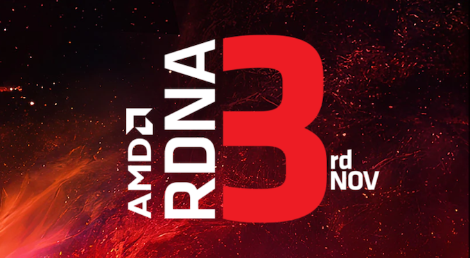
Like the Ryzen event in August, next month’s Radeon event appears to be AMD gearing up for the launch of its next generation of consumer products – this time on the GPU side of matters. Back at the start of the summer, AMD confirmed that RDNA 3 architecture products were scheduled to arrive this year, so we have been eagerly awaiting the arrival of AMD’s next generation of video cards.
Though unlike AMD’s CPU efforts, the company has been far more mum about its next-gen GPU efforts. So details in advance on what will presumably be the Radeon RX 7000 series have been limited. The biggest items disclosed thus far are that AMD is targeting another 50% increase in performance-per-watt, and that these new GPUs (Navi 3x) will be made on a 5nm process (undoubtedly TSMC’s). Past that, AMD hasn’t given any guidance on what to expect for performance.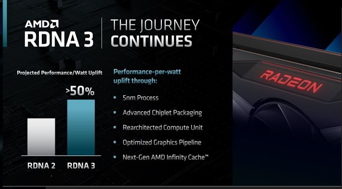
One interesting aspect, however, is that AMD has confirmed that they will be employing chiplets with this generation of products. To what extent, and whether that’s on all parts or just some, remains to be seen. But chiplets are in some respects the holy grail of GPU construction, because they give GPU designers options for scaling up GPUs past today’s die size (reticle) and yield limits. That said, it’s also a holy grail because the immense amount of data that must be passed between different parts of a GPU (on the order of terabytes per second) is very hard to do – and very necessary to do if you want a multi-chip GPU to be able to present itself as a single device.
We’re also apparently in store for some more significant upgrades to AMD’s overall GPU architecture. Though what exactly a “rearchitected compute unit” and “optimized graphics pipeline” fully entail remains to be seen.
Thankfully we should have our answer here in two weeks. The presentation is slated to air on November 3rd at 1pm Pacific, on AMD’s YouTube channel. And of course, be sure to check out AnandTech for a full rundown and analysis of AMD’s announcements.
More...
-
10-27-22, 08:07 AM #11590
Anandtech: ONYX BOOX Tab Ultra ePaper Tablet Launches with Qualcomm Snapdragon 662
The e-Paper market has enjoyed steady growth over the last decade, starting with the introduction of the Amazon Kindle back in 2007. While there are many vendors attempting to make a mark in the technology required in this space, E-Ink's offerings have ruled the roost.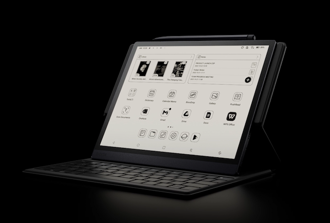
The most popular category of products using E-Ink's technology has undoubtedly been eBook readers. Recently, digital notebooks and notepads have also emerged as a significant driver in E-Ink's expansion. These products take the regular e-reader and add support for an electronic pen / stylus. These products were initially quite expensive and targeted business professionals dealing with huge amounts of paperwork and requiring note-taking support (such as lawyers). The Sony DPT lineup (review) became one of the leading products in this category. As the market expanded, vendors such as reMarkable and ONYX also started putting out compelling products - expanding the target market to creative professionals and students as well. This category became truly mass-market a few months back with the introduction of Amazon's Kindle Scribe (and slated to start shipping in time for the holiday season).
ONYX has been serving the e-reader market since 2006. They have an extensive lineup of e-readers (both grayscale and color), e-Paper tablets with note-taking support, and even E-Ink monitors. Today, the company is launching a new category - ePaper Tablet PCs. The first product in this lineup is the ONYX BOOX Tab Ultra - a 10.3" unit complete with a 16MP rear-facing camera. A first for E-Ink devices, ONYX envisages the camera being used to OCR documents in the field without the need for an external device as an intermediary. The device targets professional use-cases. It must be noted that ONYX already carries the BOOX Note Air 2 Plus that carries most of the same features, but geared towards the home / casual consumer.
The ONYX BOOX Tab Ultra is the first e-reader model from ONYX to utilize the company's proprietary fast refresh algorithm implemented using a separate hardware module on the board. The company has been using this on its Mira lineup of E-Ink monitors, and its use in the e-reader is supposed to improve user experience with web content. Scrolling, in particular, has been a weak point of E-Ink tablets due to the low refresh rate. The actual improvements delivered by the ONYX 'BSR' (BOOX Super Refresh) algorithm in this aspect needs hands-on evaluation for further analysis. The system supports four different modes for different tasks - reading books doesn't require fast refreshing and can utilize the 'HD Mode', while typing requires a 'Balance Mode'. A 'Fast Mode' is available for web browsing, and an 'Ultrafast Mode' for generic Android applications.
The BOOX Tab Ultra utilizes a Qualcomm Snapdragon 662 SoC (4x Kyro Gold (A73-class) @ 2GHz + 4x Kyro Silver (A53-class) @ 1.8 GHz, along with an Adreon 610 GPU), and comes with a specialized version of Android 11 (including Play Store support). The unit is equipped with a 6300 mAh battery, 4GB of LPDDR4x DRAM, and 128GB of eMMC flash storage. The USB-C port in the system also supports OTG functionality, and a micro-SDXC card slot. A keyboard case with a magnetic holder for the Tab Ultra is also available.
ONYX has a reputation for long support cycles, and provides regular firmware updates to augment the functionality of its ePaper tablets. Recent firmware updates have brought a more tablet-like experience in the user interface - a home screen with apps along with a favorites dock at the bottom. ONYX claims that the use of Android in its tablets (compared to custom OSes in other products such as the Kindle Scribe and reMarkable tablets) enables its customers to take advantage of the host of personal knowledge management apps available for note taking and data collection. Another recently added functionality relates to the association of different pages in different documents using easily-created tags.
The ONYX BOOX Tab Ultra is available for pre-order today and comes with a $600 price tag. The company is also simultaneously releasing the Nova Air 2 7.8" e-Paper tablet with stylus support at $400 and the Leaf 2 7" e-reader at $200. ONYX has typically not hesitated in trying out innovative ideas on the e-Paper front (they were one of the first vendors to bring out color e-readers), and equipping an e-reader / digital notebook with a rear camera is yet another interesting play from the company. The new products expand ONYX's target market and build upon its position as one of the leading E-Ink product vendors in the market in the face of rising competition.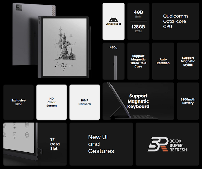
More...


 Quote
QuoteThread Information
Users Browsing this Thread
There are currently 8 users browsing this thread. (0 members and 8 guests)


Bookmarks