

Results 11,811 to 11,820 of 12089
Thread: Anandtech News
-
07-21-23, 05:36 PM #11811
Anandtech: TSMC: 3nm Chips for Smartphones and HPCs Coming This Year
While TSMC formally started mass production of chips on its N3 (3nm-class) process technology late last year, the company is set to finally ship the first revenue wafers in the current quarter. During the most recent earnings call with analysts and investors, the company said that demand for 3 nm products was steady, and that numerous designs for smartphones and high-performance applications are incoming later this year. Furthermore, N3E manufacturing node is on track for high-volume manufacturing later this year.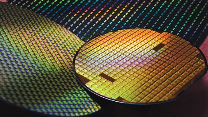
"We are seeing robust demand for N3 and we expect a strong ramp of N3 in the second half of this year, supported by both HPC and smartphone applications," said C.C. Wei, chief executive officer of TSMC, during the company's earnings. Call with financial analysts and investors.
Previously the company never commented on applications that use its initial N3 fabrication process, but for now it actually disclosed that devices that are in mass production are designed for smartphones as well as HPC applications, which is a vague term which TSMC uses to describe everything from handheld game consoles all the way to heavy-duty smartphone SoCs.
For customer privacy reasons, TSMC does not disclose which customers are using N3. Though historically, Apple has been TSMC's alpha client for its leading-edge process technologies, so they're the most likely candidate to be the biggest consumer of TSMC's N3 output.
TSMC's baseline N3 node (aka N3B) is an expensive technology to use. It features up to 25 EUV layers (according to China Renaissance and SemiAnalysis) with TSMC using EUV double-patterning on some of them to make for higher logic and SRAM transistor density than N5. EUV steps are expensive in general, and EUV double patterning drives those costs up further, which is why this fabrication process is only expected to be used by a handful of customers who are not as concerned about the high expenditure required.
For those who are more cost sensitive, there is N3E, which can 'only' use up to 19 EUV layers and does not use EUV double patterning. Good news is that TSMC expects to commence mass production on this node to Q4 2023.
N3E has passed qualification and achieved performance and yield target and will start volume production in the fourth quarter of this year," said Wei.
Source: TSMC
More...
-
07-24-23, 10:45 AM #11812
Anandtech: AMD Launches Ryzen 5 7500F in China: Zen 4 With no Integrated Graphics
Over the weekend, AMD officially listed the Ryzen 5 7500F processor on their website. Although initial reports pointed towards a China-only release, and at present, that much is true, the Ryzen 5 7500F is heading towards global availability, at least according to AMD. With a reported MSRP of around $179, the Ryzen 5 7500F is currently the cheapest Zen 4-based desktop processor. It comes with six Zen 4 cores and is similar in specifications to the Ryzen 5 7600, albeit with a few variances. Most importantly, it doesn't feature AMD's RDNA 2 integrated graphics, as seen on other Ryzen 7000 SKUs.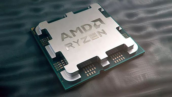
When AMD initially launched their Ryzen 7000 desktop processors based on their latest Zen 4 microarchitecture in September last year, they received many performance and power efficiency plaudits. One area that didn't shine so brightly was in value, as AMD's Ryzen 7000 processors only support DDR5, and at the time, AMD's new (at the time) AM5 platform was hardly cheap. Fast forward to now, and AMD looks to rectify that with their first sub $200 chip based on Zen 4, the Ryzen 5 7500F.
*Price as reported by Toms Hardware & TechPowerUpAMD Ryzen 5 Series Line-Up (Sub $300) AnandTech Cores
ThreadsBase
FreqTurbo
FreqMemory
SupportL3
CacheTDP PPT Price $ Ryzen 5 7600X 6C / 12T 4.7 GHz 5.3 GHz DDR5-520032 MB 105 W 142 W $299 Ryzen 5 7600 6C / 12T 3.8 GHz 5.1 GHz DDR5-520032 MB 65 W 88 W $227 Ryzen 5 7500F 6C / 12T 3.7 GHz 5.0 GHz [COLOR=text-align: center]DDR5-5200[/COLOR]32 MB 65 W 88 W $179?*
Despite only being available at the time of writing in the Chinese market, the AMD Ryzen 5 7500F benefits from six Zen 4 cores (and 12 threads), as well as a base frequency of 3.7 GHz and a turbo of up to 5.0 GHz. As with other Ryzen 5 models, such as the 7600X and 7600, the 7500F also has 32 MB of L3 cache. It also aligns with the more efficient Ryzen 5 7600 and, as such, has a 65 W base TDP with a Package Power Tracking (PPT) of up to 88 W.
The most significant difference between the Ryzen 5 7500F and the other Ryzen 7000 series processors is it seems to be the first Zen 4-based CPU to omit integrated graphics. Although the other Ryzen 7000 series chips use RDNA 2-based integrated graphics, which, although not good enough to game with at decent frame rates, does provide other benefits as it is more than powerful enough to operate typical desktop work. The Ryzen 5 7500F does retain all the other benefits of the Zen 4 and AM5 platform, such as 28 x PCIe 5.0 lanes and support for a fully-fledged high-performance PCIe 5.0 x4 M.2 SSD.
All currently associated reviews of the Ryzen 5 7500F are from Chinese and South Korean media outlets. As we mentioned, this is because, technically, the only place users can currently buy this chip is in China. Still, things point to a subsequent global launch further down the line or imminently in other regions such as North America and Europe.
More...
-
07-24-23, 06:20 PM #11813
Anandtech: Cadence Buys Memory and SerDes PHY Assets from Rambus
In a surprising turn of events, Cadence and Rambus entered into a definitive agreement late last week for Cadence to buy memory physical interface IP and SerDes businesses from Rambus. As a result, Cadence will get a comprehensive portfolio of memory PHY IP and an established client base. Meanwhile, with the sale of its PHY and SerDes assets, Rambus will now solely focus on licensing digital IP.
Historically, Rambus developed memory technologies, including RDRAM and XDR DRAM. At some point, the company patented fundamental technologies enabling SDRAM, DDR SDRAM, and their successors. Doing this allowed them to effectively sue virtually all memory makers and designers of memory controllers (including AMD and Nvidia) and make them pay license fees.
Over time the company began to license memory controllers and PHY. It became a one-stop shop for chip developers needing a turnkey memory, PCIe, or MIPI solution for their designs. Nowadays, it is possible to come to Rambus and get one of the industry's best memory controllers and silicon-proven interfaces. But while Rambus plans to retain memory and interface controllers and everything logic-related, it intends to get rid of its PHY and SerDes IP assets and sell them to Cadence.
Getting silicon-proven PHY and SerDes IP assets and clients for Cadence makes perfect sense.
"The acquisition of the Rambus PHY IP broadens Cadence's well-established enterprise IP portfolio and expands its reach across geographies and vertical markets, such as the aerospace and defense market, providing complete subsystem solutions that meet the demands of our worldwide customers," said Boyd Phelps, senior vice president and general manager of the IP Group at Cadence.
But the rationale behind Rambus's decision to sell PHY and SerDes business is less obvious. On the one hand, memory PHY and SerDes businesses require Rambus to invest in expensive tape-outs on the latest nodes, and this requires capital and increases risks as Rambus has to compete against companies like Cadence and Synopsys that are larger and have more money. On the other hand, Rambus can be a one-stop shop for memory controllers and PHY, which has advantages (i.e., Rambus can charge a premium).
Meanwhile, without needing to keep its physical IP assets up to date, Rambus can now focus on licensing pure technologies and no longer invest in physical IP like PHY or SerDes.
"With this transaction, we will increase our focus on market-leading digital IP and chips and expand our roadmap of novel memory solutions to support the continued evolution of the data center and AI," said Sean Fan, senior vice president and chief operating officer at Rambus.
The transaction is projected to have a negligible impact on the revenue and earnings of each company for this year. The anticipated closing date is in the third quarter of 2023, subject to specific closing conditions.
Source: Cadence
More...
-
07-25-23, 12:56 PM #11814
Anandtech: TACC's Stampede3 Supercomputer Uses Intel's Xeon Max with HBM2E and Ponte
The Texas Advanced Computing Center (TACC) unveiled its latest Stampede supercomputer for open science research projects, Stampede3. TACC anticipates that Stampede3 will come online this fall and will deliver its full performance in early 2024. The supercomputer will be a crucial component of the U.S. National Science Foundation’s (NSF) ACCESS scientific supercomputing ecosystem, and it is projected to serve the open science community from 2024 until 2029.
The third-generation Stampede cluster, which will be built by Dell, will incorporate 560 nodes equipped with Intel's Sapphire Rapids generation Xeon CPU Max processors, each offering 56 CPU cores and 64GB of on-package HBM2E memory. Surprisingly, TACC is going to be operating these nodes in HBM-only mode, so no additional DRAM will be attached to the CPU nodes – all of their memory will come from the on-chip HBM stacks.
With these specifications, Stampede3 is expected to have a peak performance of approximately 4 FP64 PetaFLOPS, while offering nearly 63,000 general-purpose cores. In addition, TACC also plans to install 10 Dell PowerEdge XE9640 servers with 40 Intel Data Center GPU Max compute GPUs for artificial intelligence and machine learning workloads.
Given this layout, the bulk of Stampede3's compute performance will be supplied by CPUs. This makes Stampede3 a bit of a rarity in this day and age, as most high-performance systems are GPU driven, leaving Stampede3 as one of the last supercomputers that relies almost solely on general-purpose CPUs.
And while the current cluster is primarily focused on CPU performance, TACC is also going to use the Intel GPUs in the latest Stampede revamp to investigate on how to incorporate larger numbers of GPUs into future versions of the system. For now, most of TACC's AI tasks are run on its Lone Star systems, which is powered by hundreds Nvidia A100 compute GPUs. So the organization's aim is to explore whether a portion of this workload can be transferred to Intel's Ponte Vecchio.
We are going to put in a small system with exploratory capability using Intel Ponte Vecchio," said Dan Stanzione, executive director of TACC. "We are still negotiating exactly how much of that will have, but I would say a minimum of 40 nodes and maximum of a hundred or so. […] We are just putting a couple of racks of Ponte Vecchio out there to see how people work with it."
Stampede3 will leverage 400 Gb/s Omni-Path Fabric technology that will enable a backplane bandwidth of 24TB/s. This setup will allow the machine to efficiently scale and minimize latencies, making it well-suited for various applications requiring simulations.
TACC also plans to reincorporate nodes from the previous version, Stampede2, which were based on older-generation Xeon Scalable CPUs. This integration will enhance the capacity of Stampede3 for high-memory applications, high-throughput computing, interactive workloads, and other previous-generation applications. In total, the new supercomputer system will feature 1,858 compute nodes with over 140,000 cores, more than 330 TBs of RAM, new storage capacity of 13 PBs, and a peak performance close to 10 PetaFLOPS.
Sources: TACC, HPCWire
More...
-
07-25-23, 12:56 PM #11815
Anandtech: Intel Unveils AVX10 and APX Instruction Sets: Unifying AVX-512 For Hybrid
Intel has announced two new x86-64 instruction sets designed to bolster and offer more performance in AVX-based workloads with their hybrid architecture of performance (P) and efficiency (E) cores. The first of Intel's announcements is their latest Intel Advanced Performance Extensions, or Intel APX as it's known. It is designed to bring generational, instruction set-driven improvements to load, store and compare instructions without impacting power consumption or the overall silicon die area of the CPU cores.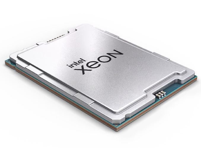
Intel has also published a technical paper detailing their new AVX10, enabling both Intel's performance (P) and efficiency (E) cores to support the converged AVX10/256-bit instruction set going forward. This means that Intel's future generation of hybrid desktop, server, and workstation chips will be able to support multiple AVX vectors, including 128, 256, and 512-bit vector sizes throughout the entirety of the cores holistically.
Intel Advanced Performance Extensions (APX): Going Beyond AVX and AMX
Intel has published details surrounding its new Advanced Performance Extensions, or APX for short. The idea behind APX is to allow access to more registers and improve overall general-purpose performance. They are designed to provide better efficiency when using x86-based instruction sets, allowing access to more registers. New features such as doubling the general-purpose registers from 16 to 32 enable compilers to keep more values within the registers, with Intel claiming 10% fewer loads and 20% fewer stores when the code is compiled for APX versus the same code for x86-64 using Intel 64; this is Intel's 64-bit compatibility mode for x86 instruction sets.
The idea behind doubling the number of GPRs from 16 with x86-64 to the 32 GPRs available with the Intel APX is that more data can be held close by, avoiding the need to read and write further into the different levels of cache and memory. Having more GPR also means that it should theoretically require less access to slower areas, such as DRAM, which takes longer and uses more power.
Despite effectively abandoning its MPX (Memory Protection Extensions), the Intel APX can effectively use the existing area set aside for MPX for what it calls XSAVE. Touching more on XSAVE, Intel's APX general purpose registers (GPRs) are XSAVE-enabled, which means they can automatically be saved and restored by XSAVE and XRSTOR sequences during context switches. Intel also states by default that these don't change the size or layout, which means they can take up the same space left behind for the now-defunct Intel MPX registers.
Another essential feature of Intel's APX is its support for three-operand instruction formats, a subset of the x86 instruction set specifying the data being operated on. APX introduces new instructions optimized for predicted loads, including a novel 64-bit absolute jump instruction. Compared to older examples that used EVEX, a 4-byte extension to VEX, APX transforms single register operands into three, effectively reducing the need for additional register move instructions. As a result, APX compiled code achieves a claimed 10% increase in efficiency, requiring 10% fewer instructions than previous ISAs.
Intel AVX10: Pushing AVX-512 through 256-bit and 512-bit Vectors
One of the most significant updates to Intel's consumer-focused instruction sets since the introduction of AVX-512 is Intel's Advanced Vector Extension 10 (AVX10). On the surface, it looks to bring forward AVX-512 support across all cores featured in their heterogeneous processor designs.
The most significant and fundamental change introduced by AVX10 compared to the previous AVX-512 instruction set is the incorporation of previously disabled AVX-512 instruction sets in future examples of heterogeneous core designs, exemplified by processors like the Core i9-12900K and the current Core i9-13900K. This enables support for AVX-512 in these processors. Currently, AVX-512 is exclusively supported on Intel Xeon performance (P) cores.
Examining the core concept of AVX10 it signifies that consumer-based desktop chips will now have full AVX-512 support. Although performance (P) cores have the theoretical capability to support 512-bit wide vectors if Intel desires (Intel has currently confirmed support is up to 256-bit vectors), efficiency (E) cores are restricted to 256-bit vectors. Nevertheless, as a whole, the entire chip will be capable of supporting complete AVX-512 instruction sets across all of the cores, whether they are fully-fledged performance or lower-powered efficiency cores.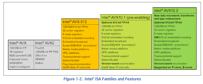
Image Source: Intel
Touching on performance, within the AVX10 technical paper, Intel states the following:
- Intel AVX2-compiled applications, re-compiled to Intel AVX10, should realize performance gains without the need for additional software tuning.
- Intel AVX2 applications sensitive to vector register pressure will gain the most performance due to the 16 additional vector registers and new instructions.
- Highly-threaded vectorizable applications are likely to achieve higher aggregate throughput when running on E-core-based Intel Xeon processors or on Intel® products with performance hybrid architecture.
Intel further claims that their chips, already utilizing 256-bit vectors as an example, will maintain similar performance levels when compiled onto AVX10 at the 256-bit ISO vector length. However, the true potential of AVX10 comes to light when leveraging the more substantial 512-bit vector length, promising the best AVX10 instruction set performance attainable. This aligns with introducing new AVX10 libraries and enhanced tool support, enabling application developers to compile newer AI and scientific-focused codes for optimal benefits. Additionally, this means preexisting libraries can be recompiled with AVX10/256 compatibility and, when possible, further optimized to exploit the larger vector units for better performance throughput.
In Intel's first phase of AVX10 (AVX10.1), this will be introduced for early software enablement and will support the subset of Intel's AVX-512 instruction sets, with Granite Rapids (6th Gen Xeon) performance (P) cores being the first cores to be forward compatible with AVX10. It is worth noting that AVX10.1 will not enable 256-bit embedded routing. As such, AVX10.1 will serve as an introduction to AVX10 to enable forward compatibility and implementation of the new versioning enumeration scheme.
Intel's 6th Gen Xeons, codenamed Granite Rapids, will enable AVX10.1, and future chips after this will bring fully-fledged AVX10.2 support, with AVX-512 also being supported to allow for compatibility for legacy instruction sets and applications compiled with them. It is worth noting that despite Intel AVX10/512 including all of Intel's AVX-512 instructions, applications compiled to Intel AVX-512 with vector lengths limited to 256-bit are not guaranteed to work with an AVX10/256 processor due to differences in the supported mask register width.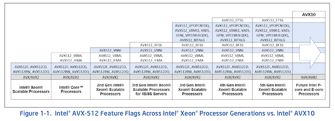
Image source: Intel
While initial support of the AVX10 instruction set is more of a transitional phase in AVX10.1, it's when AVX10.2 finally rolls out will be where AVX10 will start to show cause and effect in performance and efficiency, at least with compatible instruction sets associated with AVX10. AVX10, by default, will allow developers that recompile their preexisting code to work with AVX10, as new processors with AVX10 won't be able to run AVX-512 binaries as they previously would have. Intel is finally looking toward the future.
The introduction of AVX10 completely replaces the AVX-512 superset. Once AVX10 is widely available through Intel's future product releases, there's technically no need to use AVX-512 going forward. One challenge this presents is that software developers who have specifically compiled libraries specifically for 512-bit wide vectors will need to recompile the code as previously mentioned to properly work with the 256-bit wide vectors that AVX10 holistically supports across the cores.
While AVX-512 isn't going anywhere as an instruction set, it's worth highlighting that AVX10 is backward compatible, which is an essential aspect of supporting instruction sets with various vector widths such as 128, 256, and 512-bit where applicable. Developers can recompile code and libraries for the broader transition and convergence to the AVX10 unified instruction set going forward.
Intel is committing to supporting a maximum vector size of at least 256-bit on all Intel processors in the future. Still, it remains to be seen which SKUs (if any) and the underlying architecture will support full 512-bit vector sizes in the future, as this is something Intel hasn't officially confirmed at any point.
The meat and veg of Intel's new AVX10 instruction set will come into play when AVX10.2 is phased in, officially bringing 256-bit instruction vector support across all cores, whether performance and/or efficiency cores. This also marks the inclusion of 128-bit, 256-bit, and 512-bit integer divisions across both the performance and efficiency cores, and as such, will support full vector extensions based on the specification of each core.
More...
-
07-26-23, 12:52 PM #11816
Anandtech: Rapidus Wants to Supply 2nm Chips to Tech Giants, Challenge TSMC
It has been a couple of decades since a Japanese fab has offered a leading-edge chip manufacturing process. Even to this day, none of the Japanese chipmakers have made it as far as adopting FinFETs, something that U.S. and Taiwanese companies adopted in early-to-mid-2010s. But Rapidus, a semiconductor consortium backed by the Japanese government and large conglomerates, plans to leapfrog several generations of nodes and start 2nm production in 2027. Interestingly, the company aims to serve world's leading tech giants, challenging TSMC, IFS, and Samsung Foundry.
The endeavor is both extremely challenging and tremendously expensive. Modern fabrication technologies are expensive to develop in general. To cut down its R&D costs, Rapidus teamed up with IBM, which has done extensive research in such fields as transistor structures as well as chip materials. But in addition to developing a viable 2nm fabrication process, Rapidus will also have to build a modern semiconductor fabrication facility, which is an expensive venture. Rapidus itself projects that it will need approximately $35 billion to initiate pilot 2nm chip production in 2025, and then bring that to high-volume manufacturing in 2027.
To recover the massive R&D and fab construction costs, Rapidus will need to produce its 2nm chips in very high volumes. As demand from Japanese companies alone may not suffice, Rapidus is looking for orders from international corporations like Apple, Google, and Meta.
"We are looking for a U.S. partner, and we have begun discussions with some GAFAM [Google, Apple, Facebook, Amazon and Microsoft] corporations," Atsuyoshi Koike, chief executive of Rapidus, told Nikkei. "Specifically, there is demand [for chips] from data centers [and] right now, TSMC is the only company that can make the semiconductors they envision. That is where Rapidus will enter."
Despite escalating chip design costs, the number of companies opting to develop their own custom system-on-chips for artificial intelligence (AI) and high-performance computing (HPC) applications is growing these days. Hyperscalers like AWS, Google, and Facebook have already developed numerous chips in-house to replace off-the-shelf offerings from companies like AMD, Intel, and NVIDIA with something that suits them better.
These companies typically rely on TSMC since the latter tends to offer competitive nodes, predictable yields, and the ability to re-use IP across various products. So securing orders from a tech giant is challenging for a new kid on the block. But Rapidus' strategy is not completely unfounded, as the number of hyperscalers that need custom silicon is growing and one or two may opt for Rapidus if the Japanese company can provide competitive technology, high yields, and fair pricing.
With that said, however, Rapidus is also making it clear that the company does not plan to emulate TSMC's entire business model, where they'd serve a wide range of clients like TSMC does. Instead, Rapidus intends to start with about five customers, then gradually expand to 10, and then see if it wants and can serve more.
"Our business model is not that of TSMC, which manufactures for every client," said Koike. "We will start with around five companies at most, then eventually grow to 10 companies, and we'll see if we'll increase the number beyond that."
It is unclear whether such a limited client base can generate enough demand and revenue to recover Rapidus' massive investment needed to kick-start 2nm production by 2027. It is also going to be a challenge to secure even five significant 2nm orders by 2027 given the limited number of companies ready to invest in chips to be made on a leading-edge technology and competition from established players like TSMC, Samsung Foundry, and IFS.
However, from the Japanese government's perspective, Rapidus is seen as a catalyst for revitalizing Japan's advanced semiconductor supply chain, rather than a money making machine in and of itself. So even if the 2nm project was not an immediate success, it can be justified as a stepping stone towards creating more opportunities for local chip designers.
As for revenue, Koike predicts that quotes for its 2nm chips will be 10 times greater than for chips currently made by Japanese firms, which is of course a significant change for the Japanese chip industry. This is not particularly surprising though, as the most advanced process technology available in Japan today is 45nm, which these days is a very inexpensive node as it is used on fully depreciated fabs and does not require any new equipment.
Sources: Nikkei, DigiTimes
More...
-
07-26-23, 12:52 PM #11817
Anandtech: Micron Unveils HBM3 Gen2 Memory: 1.2 TB/sec Memory Stacks For HPC and AI P
Micron today is introducing its first HBM3 memory products, becoming the latest of the major memory manufacturers to start building the high bandwidth memory that's widely used in server-grade GPUs and other high-end processors. Aiming to make up for lost time against its Korean rivals, Micron intends to essentially skip "vanilla" HBM3 and move straight on to even higher bandwidth versions of the memory they're dubbing "HBM3 Gen2", developing 24 GB stacks that run at over 9 GigaTransfers-per-second. These new HBM3 memory stacks from Micron will target primarily AI and HPC datacenter, with mass production kicking off for Micron in early 2024.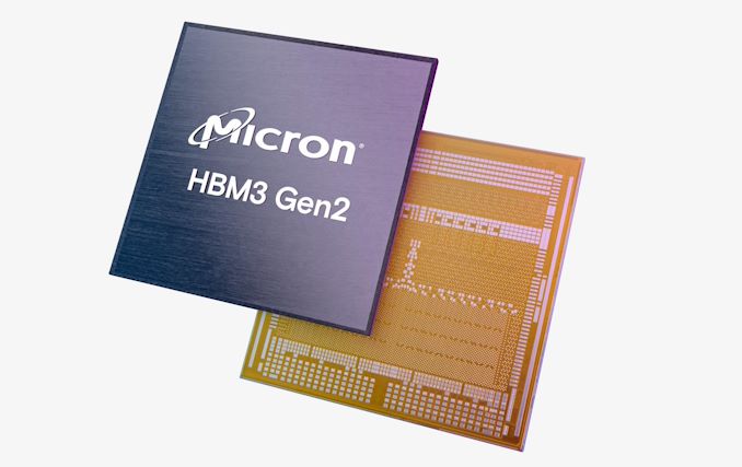
Micron's 24 GB HBM3 Gen2 modules are based on stacking eight 24Gbit memory dies made using the company's 1β (1-beta) fabrication process. Notably, Micron is the first of the memory vendors to announce plans to build HBM3 memory with these higher-density dies, while SK hynix offers their own 24 GB stacks, the company is using a 12-Hi configuration of 16Gbit dies. So Micron is on track to be the first vendor to offer 24 GB HBM3 modules in the more typical 8-Hi configuration. And Micron is not going to stop at 8-Hi 24Gbit-based HBM3 Gen2 modules, either, with the company saying that they plan to introduce even higher capacity class-leading 36 GB 12-Hi HBM3 Gen2 stacks next year.
Besides taking the lead in density, Micron is also looking to take a lead in speed. The company expects its HBM3 Gen2 parts to hit date rates as high as 9.2 GT/second, 44% higher than the top speed grade of the base HBM3 specification, and 15% faster than the 8 GT/second target for SK hynix's rival HBM3E memory. The increased data transfer rate enables each 24 GB memory module to offer peak bandwidth of 1.2 TB/sec per stack.
Micron says that 24GB HBM3 Gen2 stacks will enable 4096-bit HBM3 memory subsystems with a bandwidth of 4.8 TB/s and 6096-bit HBM3 memory subsystems with a bandwidth of 7.2 TB/s. To put the numbers into context, Nvidia's H100 SXM features a peak memory bandwidth of 3.35 TB/s.
High frequencies aside, Micron's HBM3 Gen2 stacks are otherwise drop-in compatible with current HBM3-compliant applications (e.g., compute GPUs, CPUs, FPGAs, accelerators). So device manufacturers will finally have the option of tapping Micron as an HBM3 memory supplier as well, pending the usual qualification checks.HBM Memory Comparison "HBM3 Gen2" HBM3 HBM2E HBM2 Max Capacity 24 GB 24 GB 16 GB 8 GB Max Bandwidth Per Pin 9.2 GT/s 6.4 GT/s 3.6 GT/s 2.0 GT/s Number of DRAM ICs per Stack 8 12 8 8 Effective Bus Width 1024-bit Voltage 1.1 V? 1.1 V 1.2 V 1.2 V Bandwidth per Stack 1.2 TB/s 819.2 GB/s 460.8 GB/s 256 GB/s
Under the hood, Micron's goal to jump into an immediate performance leadership position within the HBM3 market means that they need to one-up their competition from a technical level. Among other changes and innovations to accomplish that, the company increased the number of through-silicon vias (TSVs) by two times compared to shipping HBM3 products. In addition, Micron shrunk the distance between DRAM devices in its HBM3 Gen2 stacks. These two changes to packaging reduced thermal impendence of these memory modules and made it easier to cool them down. Yet, the increased number of TSVs can bring other advantages too.
Given that Micron uses 24 Gb memory devices (rather than 16 Gb memory devices) for its HBM3 Gen2 stacks, it is inevitable that it had to increase the number of TSVs to ensure proper connectivity. Yet, doubling the number of TSVs in an HBM stack can enhance overall bandwidth (and shrink latency), power efficiency, and scalability by facilitating more parallel data transfers. It also improves reliability by mitigating the impact of single TSV failures through data rerouting. However, these benefits come with challenges such as increased manufacturing complexity and increased potential for higher defect rates (already an ongoing concern for HBM), which can translate to higher costs.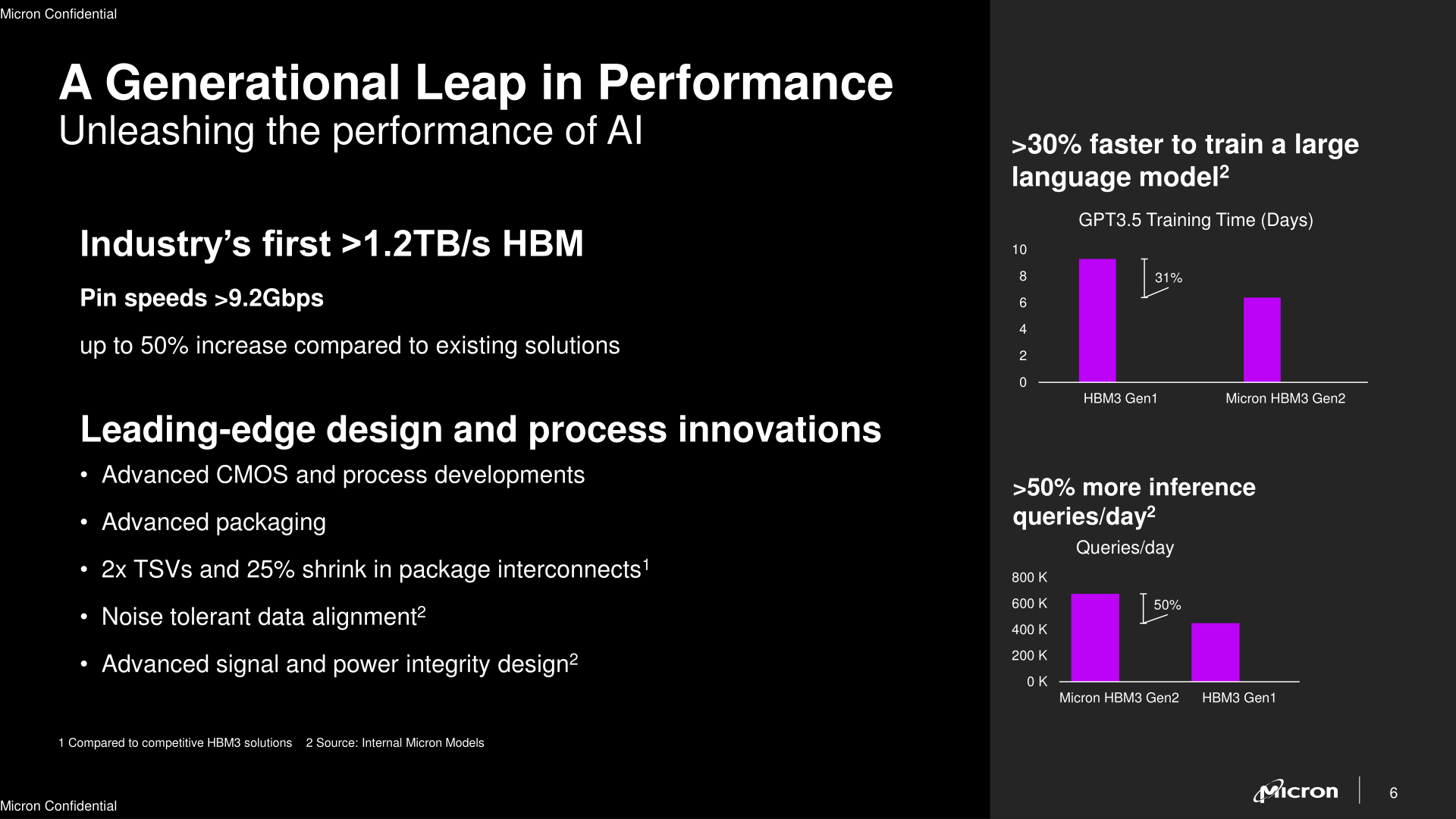
Just like other HBM3 memory modules, Micron's HBM3 Gen2 stacks feature Reed-Solomon on-die ECC, soft repair of memory cells, hard-repair of memory cells as well as auto error check and scrub support.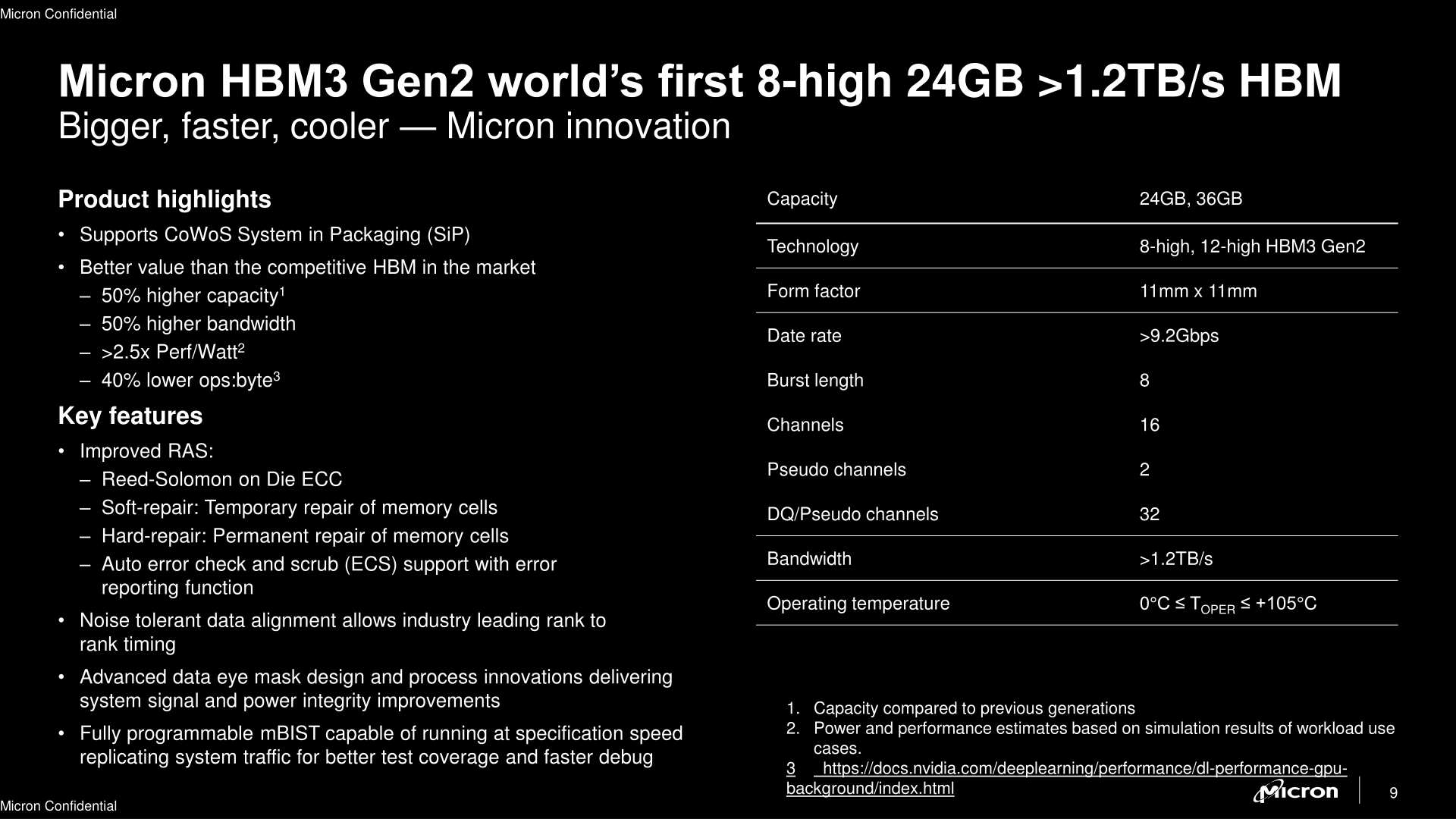
Micron says it will mass produce its 24 GB HBM3 modules starting in Q1 2024, and will start sampling its 12-Hi 36GB HBM3 stacks around this time as well. The latter will enter high volume production in the second half of 2024.
To date, the JEDEC has yet to approve a post-6.4GT/second HBM3 standard. So Micron's HBM3 Gen2 memory, as well as SK hynix's rival HBM3E memory, are both off-roadmap standards for the moment. Given the interest in higher bandwidth HBM memory and the need for standardization, we'd be surprised if the group didn't eventually release an updated version of the HBM3 standard that Micron's devices will conform to. Though as the group tends to shy away from naming battles ("HBM2E" was never a canonical product name for faster HBM2, despite its wide use), it's anyone's guess how this latest kerfuffle over naming will play out.
Beyond their forthcoming HBM3 Gen2 products, Micron is also making it known that the company already working on HBMNext (HBM4?) memory. That iteration of HBM will provide 1.5 TB/s – 2+ TB/s of bandwidth per stack with capacities ranging from 36 GB to 64 GB.
More...
-
07-27-23, 05:52 PM #11818
Anandtech: Micron Publishes Updated DRAM Roadmap: 32 Gb DDR5 DRAMs, GDDR7, HBMNext
In addition to unveiling its first HBM3 memory products yesterday, Micron also published a fresh DRAM roadmap for its AI customers for the coming years. Being one of the world's largest memory manufacturers, Micron has a lot of interesting things planned, including high-capacity DDR5 memory devices and modules, GDDR7 chips for graphics cards and other bandwidth-hungry devices, as well as HBMNext for artificial intelligence and high-performance computing applications.
32 Gb DDR5 ICs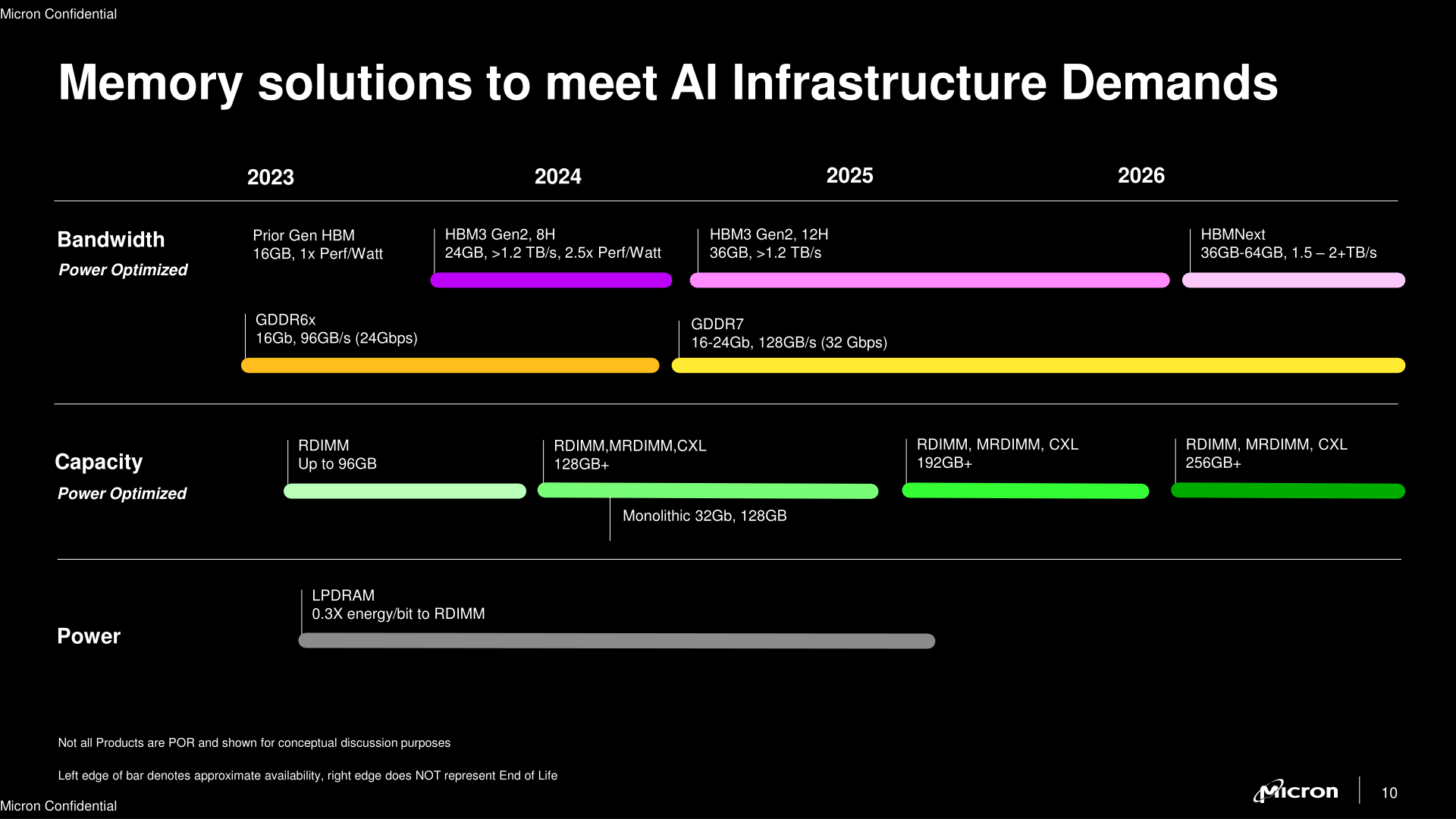
We all love inexpensive high-capacity memory modules, and it looks like Micron has us covered. Sometimes in the late first half of 2024, the company plans to roll-out its first 32 Gb DDR5 memory dies, which will be produced on the company's 1β (1-beta) manufacturing process. This is Micron's latest process node and which does not use extreme ultraviolet lithography, but rather relies on multipatterning.
32 Gb DRAM dies will enable Micron to build 32 GB DDR5 modules using just eight memory devices on one side of the module. Such modules can be made today with Micron's current 16 Gb dies, but this requires either placing 16 DRAM packages over both sides of a memory module – driving up production costs – or by placing two 16 Gb dies within a single DRAM package, which incurs its own costs due to the packaging required. 32 Gb ICs, by comparison, are easier to use, so 32 GB modules based on denser DRAM dies will eventually lead to lower costs compared to today's 32 GB memory sticks.
But desktop matters aside, Micron's initial focus with their higher density dies will be to build even higher capacity data center-class parts, including RDIMMs, MRDIMMs, and CXL modules. Current high performance AI models tend to be very large and memory constrained, so larger memory pools open the door both to even larger models, or in bringing down inference costs by being able to run additional instances on a single server.
For 2024, Micron is planning to release 128GB DDR5 modules based on these new dies. In addition, the company announced plans for 192+ GB and 256+ GB DDR5 modules for 2025, albeit without disclosing which chips these are set to use.
Meanwhile, Micron's capacity-focused roadmap doesn't have much to say about bandwidth. While it would be unusual for newer DRAM dies not to clock at least somewhat higher, memory manufacturers as a whole have not offered much guidance about future DDR5 memory speeds. Especially with MRDIMMs in the pipeline, the focus is more on gaining additional speed through parallelism, rather than running individual DRAM cells faster. Though with this roadmap in particular, it's clear that Micron is more focused on promoting DDR5 capacity than promoting DDR5 performance.
GDDR7 in 1H 2024
Micron was the first larger memory maker to announce plans to roll out its GDDR7 memory in the first half of 2024. And following up on that, the new roadmap has the the company prepping 16 Gb and 24 Gb GDDR7 chips for late Q2 2024.
As with Samsung, Micron's plans for their first generation GDDR7 modules do not have them reaching the spec's highest transfer rates right away (36 GT/sec), and instead Micron is aiming for a more modest and practical 32 GT/sec. Which is still good enough to enable upwards of 50% greater bandwidth for next-generation graphics processors from AMD, Intel, and NVIDIA. And perhaps especially NVIDIA, since this roadmap also implies that we won't be seeing a GDDR7X from Micron, meaning that for the first time since 2018, NVIDIA won't have access to a specialty GDDR DRAM from Micron.
HBMNext in 2026
In addition to GDDR7, which will be used by graphics cards, game consoles, and lower-end high-bandwidth applications like accelerators and networking equipment, Micron is also working on the forthcoming generations of its HBM memory for heavy-duty artificial intelligence (AI) and high-performance computing (HPC) applications.
Micron expects its HBMNext (HBM4?) to be available in 36 GB and 64 GB capacities, which points to a variety of configurations, such as 12-Hi 24 Gb stacks (36 GB) or 16-Hi 32 Gb stacks (64 GB), though these are pure speculations at this point. As for performance, Micron is touting 1.5 TB/s – 2+ TB/s of bandwidth per stack, which points to data transfer rates in excess of 11.5 GT/s/pin.
More...
-
07-28-23, 12:31 AM #11819
Anandtech: AMD Announces Ryzen 9 7945HX3D: Ryzen Mobile Gets 3D V-Cache
For this year's ChinaJoy expo, AMD is taking to the show to announce a new and very special mobile CPU for high-end, desktop replacement-class laptops: the Ryzen 9 7945HX3D, AMD's first V-cache-equipped mobile CPU. Slated to launch on August 22nd, the new chip is set to break new ground for AMD in the mobile space, all the while giving gamers an even more potent CPU for high-end gaming laptops.
Based on AMD's cutting-edge 3D V-Cache packaging technology, which places an additional slice of L3 cache on top of the existing L3 cache on the core complex die (CCD), the Ryzen 9 7945HX3D marks the first time AMD has brought their extended L3 cache technology to the mobile space. And like the Ryzen desktop parts already featuring this cache, such as the Ryzen 9 7950X3D, AMD's aim is to offer buyers – and especially gamers – a top-end part that can offer even better performance in select classes of workloads that can take advantage of the additional cache.
The Ryzen 9 7945HX3D is joining AMD's current lineup of desktop replacement-class mobile SKUs, the Ryzen 7045HX 'Dragon Range' series, as its new flagship mobile part. First introduced earlier this year, the AMD Ryzen 7045HX series is designed to offer desktop-grade hardware and desktop-like performance, marking the first time in the Zen era that AMD has offered its desktop silicon in a mobile chip. The entirety of the 7045HX series is based on repacked desktop silicon, and the new Ryzen 9 7945HX3D is no exception – for all practical purposes, we're essentially looking at a mobilized version of AMD flagship desktop part, the Ryzen 9 7950X3D.
More...
-
07-28-23, 07:53 AM #11820
Anandtech: Seagate Ships First Commercial HAMR Hard Drives
Seagate announced this week that it had begun the first commercial revenue shipments of its next-generation HAMR hard drives, which are being shipped out as part of Seagate's latest Corvault storage systems. This commercialization marks an important milestone in the HDDs market, as heat-assisted magnetic recording (HAMR) is expected to enable hard drives with capacities of 50 TB and beyond. Meanwhile, HDDs employing perpendicular magnetic recording (PMR) and shingled magnetic recording (SMR) technologies are expected to remain on the market for the foreseeable future.
"We shipped our first HAMR-based Corvault system for revenue as planned during the June quarter," said Gianluca Romano, chief financial officer of Seagate, at the company's earnings call. "We expect broader availability of these CORVAULT systems by the end of calendar 2023."
Seagate officially disclosed in early June that its first HAMR-based HDDs feature a 32 TB capacity and use a familiar 10-platter platform. Meanwhile, the company refrained from releasing specific capacity details of the HAMR hard drives used in these revenue Corvault systems.
Beyond Corvault systems, Seagate also shipped its HAMR-based hard drives to key customers among hyper scalers for testing and evaluation. Hyperscalers, due to their extensive storage requirements, are expected to benefit significantly from capacity points exceeding 30 TB. Though with the new technology at hand, as well as slightly higher power requirements for HAMR drives than standard PMR and SMR hard drives, the hyperscalers are also playing it safe and thoroughly validating the drives to ensure consistent performance.
Seagate's initial 32 TB HAMR hard drives will use the company's 10-platter platform, a system already proven and currently in use. Using an established platform, Seagate effectively mitigates numerous potential points of failure, potentially ensuring predictable production yield. This is smart, given the introduction of new media and write heads with its HAMR hard drives. The same 10-platter platform is expected to be used for 36 TB, 40 TB, and even larger-capacity hard drives in the future with as few alterations as possible.
"[We are] delivering on our 30+ TB HAMR product development and qualification milestones, with volume ramp on track to begin in early calendar 2024," said Dave Mosley, chief executive officer of Seagate."[…] Initial customer qualifications are progressing well. We are on track to begin volume ramp in early calendar 2024. We are also preparing qualifications with more customers, including testing for lower capacity drives targeting VIA and enterprise OEM workloads."
Even though high-volume production of HAMR hard drives is slated to begin in roughly half a year, Seagate also reaffirmed its plans for another generation of PMR and SMR hard drives during the call. These HDDs target customers not yet ready to switch to HAMR technology.
According to Seagate, they plan to introduce 24TB+ drives featuring PMR technology with two-dimensional magnetic recording (TDMR) read heads and SMR+TDMR in the near future.
"Development efforts on what may be our last PMR product are nearing completion and will extend drive capacities into the mid-to-upper 20TB range," Mosley said.
More...


 Quote
Quote


Thread Information
Users Browsing this Thread
There are currently 26 users browsing this thread. (0 members and 26 guests)


Bookmarks