

Results 12,011 to 12,020 of 12089
Thread: Anandtech News
-
01-25-24, 07:18 PM #12011
Anandtech: Intel's First High-Volume Foveros Packaging Facility, Fab 9, Starts Operat
Intel this week has started production at Fab 9, the company's latest and most advanced chip packaging plant. Joining Intel's growing collection of facilities in New Mexico, Fab 9 is tasked with packaging chips using Intel's Foveros technology, which is currently used to build the company's latest client Core Ultra (Meteor Lake) processors and Data Center Max GPU (Ponte Vecchio) for artificial intelligence (AI) and high-performance computing (HPC) applications.
The fab near Rio Rancho, New Mexico, cost Intel $3.5 billion to build and equip. The high price tag of the fab – believed to be the single most expensive advanced packaging facility ever built – underscores just how serious Intel is regarding its advanced packaging technologies and production capacity. Intel's product roadmaps call for making significant use of multi-die/chiplet designs going forward, and coupled with Intel Foundry Services customers' needs, the company is preparing for a significant jump in production volumes for Foveros, EMIB, and other advanced packaging techniques.
Intel's Foveros is a die-to-die stacking technology that uses a base die produced using the company's low-power 22FFL fabrication process and chiplet dies stacked on top of it. The base die can act like an interconnection between the dies it hosts, or can integrate certain I/O or logic. The current generation Foveros supports bumps that are as small as 36 microns and can enable up to 770 connections per square millimeter, but as the bumps become 25 and 18 microns eventually, the technology will increase connection density and performance (both in terms of bandwidth and in terms of supported power delivery).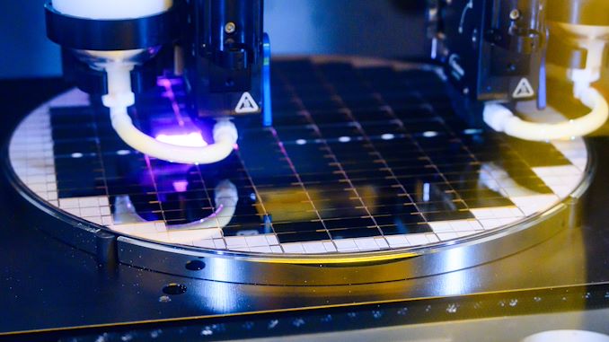
A Foveros base die can be as big as 600 mm2, but for applications that require base dies larger than 600 mm2 (such as those used for datacenter products), Intel can stitch multiple base dies together using co-EMIB packaging technology.
Finally coming into full production, the new Fab 9 (which has inherited its name from what was once a 6-inch wafer lithography fab) is slated to be Intel's crown jewel for Foveros chip packaging for at least the next couple of years. While the company has "advanced packaging" capabilities in Malaysia (PGAT) as well, those facilities are currently only tooled for EMIB production, meaning that all of Intel's Foveros packaging is taking place on its New Mexico campus. As Intel's first high-volume Foveros packaging facility, the additional capacity should greatly expand Intel's total Foveros packaging throughput, though the company isn't providing specific volume figures.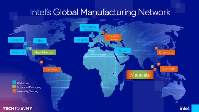
With Intel's Fab 11x directly next door, the pair of facilities are also Intel's first co-located packaging advanced packaging site, allowing Intel to cut down on how many dies they have to import from other Intel fabs. Though as Fab 11x is not an Intel 4 facility, in the case of Meteor Lake it is only suitable for producing the 22FFL base die. Intel is still importing the Intel 4-built CPU die (Oregon & Ireland), as well as the TSMC-manufactured graphics, SoC, and I/O dies (Taiwan).
"Today, we celebrate the opening of Intel's first high-volume semiconductor operations and the only U.S. factory producing the world's most advanced packaging solutions at scale," said Keyvan Esfarjani, Intel executive vice president and chief global operations officer. "This cutting-edge technology sets Intel apart and gives our customers real advantages in performance, form factor and flexibility in design applications, all within a resilient supply chain. Congratulations to the New Mexico team, the entire Intel family, our suppliers, and contractor partners who collaborate and relentlessly push the boundaries of packaging innovation."
More...
-
01-26-24, 10:32 AM #12012
Anandtech: TeamGroup Reveals 14GB/s Innogrit IG5666-Based T-Force Ge Pro PCIe 5.0 SSD
Virtually all client SSDs with a PCIe 5.0 x4 interface released to date use Phison's PS5026-E26 controller. Apparently, TeamGroup decided to try something different and introduced a drive powered by a completely different platform, the Innogrit IG5666. The T-Force Ge Pro SSD not only uses an all-new platform, but it also boasts with fast 3D NAND to enable a sequential read speed of up to 14 GB/s, which almost saturates the PCIe 5.0 x4 bus.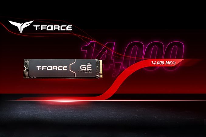
TeamGroup's T-Force Ge Pro PCIe 5.0 SSDs will be among the first drives to use the Innogrit IG5666 controller, which packs multiple cores that can handle an LDPC ECC algorithm with a 4096-bit code length, features low power consumption, has eight NAND channels, is made on a 12 nm-class process technology, and has a PCIe 5.0 x4 host interface. The drives will be available in 1 TB, 2 TB, and 4 TB configurations as well as will rely on high-performance 3D TLC NAND memory with a 2400 MT/s interface speed to guarantee maximum performance.
Indeed, 2 TB and 4TB T-Force Ge Pro drives are rated for an up to 14,000 MB/s sequential read speed as well as an up to 11,800 MB/s sequential write speed, which is in line with the highest-end SSDs based on the Phison E26 controller. Meanwhile, TeamGroup does not disclose random performance offered by these SSDs.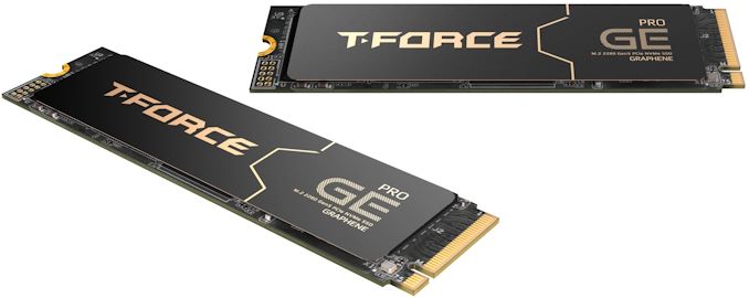
What is noteworthy is that to T-Force Ge Pro drives are equipped with a simplistic graphene heatspreader, which is said to be enough to sustain such high-performance levels under loads. Usage of such a cooler makes it easy to fit a T-Force Ge Pro into almost any system, a major difference with many of Phison E26-based drives. Of course, only reviews will reveal whether such a cooling system is indeed enough to properly cool the SSDs, but the fact that TeamGroup decided to go with a thin cooler is notable.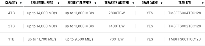
TeamGroup is set to offer its T-Force Ge Pro SSDs with a five-year warranty. Amazon, Newegg, and Amazon Japan will start taking pre-orders on these drives on February 9, 2024. Prices are currently unknown.
More...
-
01-30-24, 03:17 AM #12013
Anandtech: AMD Ryzen 7 8700G and Ryzen 5 8600G Review: Zen 4 APUs with RDNA3 Graphics
One of the most desired desktop chips designed for low-cost systems has been AMD's APUs or Accelerated Processing Units. The last time we saw AMD launch a series of APUs for desktops was back in 2021, with the release of their Cezanne-based Ryzen 5000G series, which combined Zen 3 cores with Radeon Vega-based integrated graphics. During CES 2024, AMD announced the successor to Cezanne, with new Phoenix-based APUs, aptly named the Ryzen 8000G series.
The latest Ryzen 8000G series is based on their mobile Phoenix architecture and has been refitted for AMD's AM5 desktop platform. Designed to give users and gamers on a budget a pathway to build a capable yet cheaper system without the requirement of a costly discrete graphics card hanging over their head, the Ryzen 8000G series consists of three SKUs, ranging from an entry-level Phoenix 2 based Zen 4 and Zen 4c hybrid chip, all the way to a full Zen 4 8C/16T model with AMD's latest mobile RDNA3 integrated graphics.
The Ryzen 7 8700G with 8C/16T, 16 MB of L3 cache, and AMD's Radeon 780M graphics are sitting at the top of the pile. The other chip we're taking a look at today is the middle-of-the-road AMD Ryzen 5 8600G, which has a 6C/12T configuration with fully-fledged mobile Zen 4 cores, with a third option limited to just OEMs currently, with four cores, including one full Zen 4 core and three smaller and more efficient Zen 4c cores.
The other notable inclusion of AMD's Ryzen 8000G series is it brings their Ryzen AI NPU into the desktop market for the first time. It is purposely built for AI inferencing workloads such as Generative AI and is optimized and designed to be more efficient and improve AI performance.
Much of the onus on the capability of AMD's Ryzen 8000G series will be how much of an impact the switch to Zen 4 and RDNA3 integrated graphics commands over the Ryzen 5000G series with Zen 3 and Vega, which is already three years old at this point. The other element is how the mobile-based Phoenix Zen 4 cores compare to the full-fat Raphael Zen 4 cores. In our review and analysis of the AMD Ryzen 7 8700G and Ryzen 5 8600G APUs, we aim to find out.
More...
-
01-31-24, 12:14 PM #12014
Anandtech: Corsair Launches MP600 Elite: Inexpensive Phison E27T-Based Drives
While enthusiasts are now focused mostly on SSDs with a PCIe 5.0 interface, there are many people who will be just fine with drives featuring a PCIe 4.0 interface to upgrade their PlayStation 5 or PCs bought a few years ago. To address these customers, SSD makers need to offer something that offers the right balance between price and performance. This is exactly what Corsair does with its MP600 Elite devices.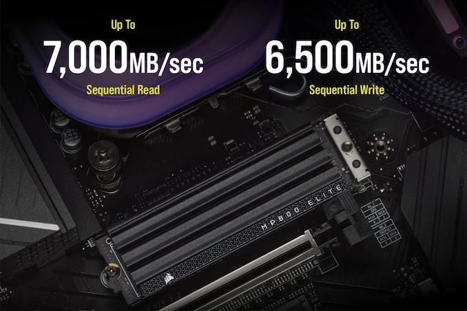
Corsair this week has released a new line of SSDs aimed at the mainstream market, the MP600 Elite. The drives are based on Phison's low-power highly-integrated PS5027-E27T platform, which is geared towards building mainstream, DRAM-less drives. The controller supports both 3D TLC and 3D QLC NAND flash via a four channel, Toggle 5.0/ONFi 5.0 interface, with data transfer rates up to 3600 MT/s. Meanwhile host connectivity is provided via a PCIe 4.0 x4 interface.
With its MP600 Elite SSDs, Corsair is not trying to offer the fastest PCIe Gen4 drives on the market, but rather attempts to offer the maximum value for 3D TLC-powered 1 TB, 2 TB as well as 4 TB configurations. The drives will offer sequential read performance of up to 7,000 MB/s and write performance of up to 6,500 MB/s, as well as random read and write speeds of up to 1,000K and 1,200K IOPS respectively, which is not bad for a PCIe Gen4 SSDs.
To maximize compatibility of its MP600 Elite drives (and make it compatible with Sony's PlayStation 5 and PlayStation 5 Slim), Corsair offers them both with a tiny aluminum heatspreader and an even thinner graphene heatspreader.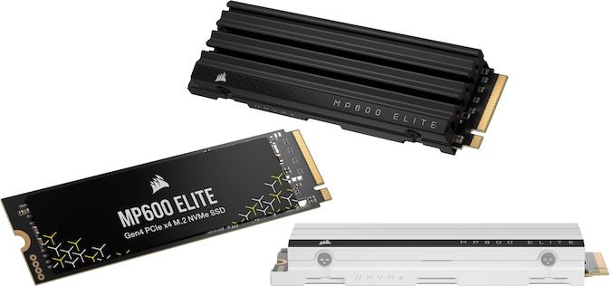
The main idea behind the Corsair MP600 Elite is its affordability: it does not require DRAM or a sophisticated cooling system, which optimizes the manufacturer's costs. Meanwhile, Corsair offers 1 TB MP600 Elite SSD with a graphene heatspreader for $89.99 and 2 TB MP600 Elite SSD with a graphene heatspreader for $164.99 (whereas versions with an aluminum heatsink are $5 cheaper), which is not particularly cheap. For example, a faster Corsair MP600 Pro LPX 2 TB costs $169.99.
Every drive is comes with a five-year warranty and can endure up to 1,200 terabytes written (TBW).
More...
-
02-02-24, 12:43 PM #12015
Anandtech: AMD Set to Fix Ryzen 8000G APU STAPM Throttling Issue, Sustained Loads Aff
Earlier this week, we published our review of AMD's latest Zen 4 based APUs, the Ryzen 7 8700G and Ryzen 5 8600G. While we saw much better gaming performance using the integrated graphics compared to the previous Ryzen 5000G series of APUs, including the Ryzen 7 5700G, the team over at Gamers Nexus has since highlighted an issue with Skin Temperature-Aware Power Management, or STAPM, for short. This particular issue is something we have investigated ourselves, and we can confirm that there is a throttling issue within the current firmware (at the time of writing) with AMD's Ryzen 8000G APUs.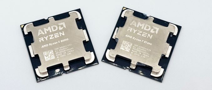
First, it's essential to understand what the Skin Temperature-Aware Power Management (STAPM) feature is and what it does. Introduced by AMD in back 2014, STAPM is a key feature within their mobile processors. STAPM extends the on-die power management by considering the processor's internal temperatures taken by on-chip thermal diodes and the laptop's surface temperature (i.e. the skin temperature). The primary goal of STAPM is to prevent laptops from becoming uncomfortably warm for users, allowing the processor to actively throttle back its heat generation based on the thermal parameters between the chassis and the processor itself.
This is where things relate directly to AMD's Ryzen 8000G series APUs. The Ryzen 8000G series of APUs is based on AMD's Phoenix silicon, which is already in use in their Ryzen Mobile 7040/8040 chips. Which means all of AMD's initial engineering for the platform was for mobile devices, and then extended to the Ryzen 8000G desktop platform. Besides the obvious physical differences, the Ryzen 8000G APUs feature a much higher 65 W TDP (88W PPT) to reflect their desktop-focused operation, making these chips the least power constrained version of Phoenix to date.
The issue is that AMD has essentially 'forgotten' to disable these STAPM features within their firmware, causing both the Ryzen 8000G APUs' Zen 4 cores and RDNA3 integrated graphics to throttle after prolonged periods of sustained load. As we can see from our investigation of the issue, in F1 2023 at 720p High settings, within 3 minutes of playing, we saw a drop in power by around 22%, which will undoubtedly impact both CPU and the integrated graphics performance during prolonged periods.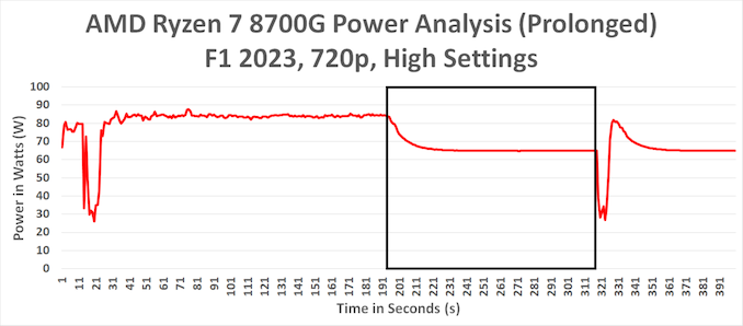
This directly affects the data in our review of the AMD Ryzen 7 8700G and Ryzen 5 8600G APUs, as the STAPM issues inherently mean that in very prolonged cases, the results may vary. Unfortunately, this issue apparently affects all AM5 motherboards and BIOSes currently available, so there's no way to properly run a Ryzen 8000G chip without STAPM throttling for the time being.
For the moment, we're putting a disclaimer on our Ryzen 8000G review, noting the issue. Once a fix is available from AMD, we'll be going back and re-testing the two chips we have to collect proper results, as well as to better quantify the performance impact of this unnecessary throttling.
Meanwhile, we reached out to AMD to confirm the issue officially, and a few minutes ago the company got back to us with a response.
"It has come to our attention that STAPM limits are being incorrectly applied to 8000 Series processors. This is causing them to drop their PPT limits under sustained load. We are working on a BIOS update to correct this behavior."The fix that AMD will seemingly apply is through updated AGESA firmware, which, from their standpoint, should be simple in practice. Perhaps the biggest outstanding question is when this fix is coming, though we can't imagine AMD taking too long with this matter.
We must also thank Gamers Nexus for highlighting and providing additional context to the STAPM-related problems from which the Ryzen 8000G APUs suffer from. The video review from Gamers Nexus of the AMD Ryzen 7 8700G and Ryzen 5 8600 APU can be found above. Once a firmware fix has been provided, we will update our data set within our review of the Ryzen 7 8700G and Ryzen 5 8600G.
More...
-
02-02-24, 12:43 PM #12016
Anandtech: AMD: Zen 5-Based CPUs for Client and Server Applications On-Track for 2024
As part of their quarterly earnings call this week, AMD re-emphasized that its Zen 5-architecture processors for both client and datacenter applications will be available this year. While the company is not making any new disclosured on products or providing a timeline beyond "later this year", the latest statement from AMD serves as a reiteration of AMD's plans, and confirmation that those plans are still on schedule.
So far, we have heard about three Zen 5-based products from AMD: the Strix Point accelerated processing units (APUs) for laptops (and perhaps eventually desktops), the Granite Ridge processors for enthusiast-grade desktops, and Turin CPUs for datacenters. During the conference call with analysts and investors, AMD's Lisa Su confirmed plans to launch Turin and Strix this year.
"Looking ahead, customer excitement for our upcoming Turin family of EPYC processors is very strong," said Lisa Su, chief executive officer of AMD, at the company's earnings call this week (via SeekingAlpha). "Turin is a drop-in replacement for existing 4th Generation EPYC platforms that extends our performance, efficiency and TCO leadership with the addition of our next-gen Zen 5 core, new memory expansion capabilities, and higher core counts."
The head of AMD also confirmed that Turin will be drop-in compatible with existing SP5 platforms (i.e., will come in an LGA 6096 package), feature more than 96 cores, and more memory expansion capabilities (i.e., enhanced support for CXL and perhaps support for innovative DIMMs). Meanwhile, the new CPUs will also offer higher per-core performance and higher performance efficiency.
As far as Strix Point is concerned, Lisa Su confirmed that this is a Zen 5 part featuring an 'enhanced RDNA 3' graphics core (also known as Navi 3.5), and an updated neural processing unit.
"Strix combines our next-gen Zen 5 core with enhanced RDNA graphics and an updated Ryzen AI engine to significantly increase the performance, energy efficiency, and AI capabilities of PCs," Su said. "Customer momentum for Strix is strong with the first notebooks on track to launch later this year."
It's notable that the head of AMD did not mention Granite Ridge CPUs foe enthusiast-grade desktops during the conference call. Though as desktop CPUs tend to have smaller margins than mobile or server parts, they are often AMD's least interesting products to investors. Despite that omission, AMD has always launched their consumer desktop chips ahead of their server chips – in part due to the longer validation times required on the latter – so Turin being confirmed for 2024 is still a positive sign for Granite Ridge.
More...
-
02-03-24, 07:48 AM #12017
Anandtech: Palit Releases Fanless Version of NVIDIA's New GeForce RTX 3050 6GB
NVIDIA today is quietly launching a new entry-level graphics card for the retail market, the GeForce RTX 3050 6GB. Based on a cut-down version of their budget Ampere-architecture GA107 GPU, the new card brings what was previously an OEM-only product to the retail market. Besides adding another part to NVIDIA's deep product stack, the launch of the RTX 3050 6GB also comes with another perk: lower power consumption thanks to this part targeting system installs where an external PCIe power connector would not be needed. NVIDIA's partners, in turn, have not wasted any time in taking advantage of this, and today Palit is releasing its first fanless KalmX board in years: the GeForce RTX 3050 KalmX 6GB.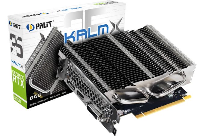
The GeForce RTX 3050 6GB is based on the GA107 graphics processor with 2304 CUDA cores, which is paired with 6GB of GDDR6 attached to a petite 96-bit memory bus (versus 128-bit for the full RTX 3050 8GB). Coupled with a boost clock rating of just 1470 MHz, the RTX 3050 6GB delivers tangibly lower compute performance than the fully-fledged RTX 3050 — 6.77 FP32 TFLOPS vs 9.1 FP32 TFLOPS — but these compromises offer an indisputable advantage: a 70W power target.
Palit is the first company that takes advantage of this reduced power consumption of the GeForce RTX 3050 6 GB, as the company has launched a passively cooled graphics card based on this part, the first in four years. The Palit GeForce RTX 3050 KalmX 6GB (NE63050018JE-1170H) uses a custom printed circuit board (PCB) that not only offers modern DisplayPort 1.4a and HDMI 2.1 outputs, but, as we still see in some entry-level cards, a dual-link DVI-D connector (a first for an Ampere-based graphics card).
The dual-slot passive cooling system with two heat pipes is certainly the main selling point of Palit's GeForce RTX 3050 KalmX 6GB. The product is pretty large though — it measures 166.3×137×38.3 mm — and will not fit into tiny desktops. Still, given the fact that fanless systems are usually not the most compact ones, this may not be a significant limitation of the new KalmX device.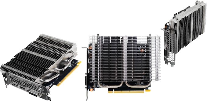
Another advantage of Palit's GeForce RTX 3050 KalmX 6GB in particular and NVIDIA's GeForce RTX 3050 6GB in general is that it can be powered entirely via a PCIe slot, which eliminates the need for an auxiliary PCIe power connectors (which are sometimes not present in cheap systems from big OEMs).
Wccftech reports that NVIDIA's GeForce RTX 3050 6GB graphics cards will carry a recommended price tag of $169 and indeed these cards are available for $170 - $180. This looks to be a quite competitive price point as the product offers higher compute performance than that of AMD's Radeon RX 6400 ($125) and Radeon RX 6500 XT ($140). Meanwhile, it remains to be seen how much will Palit charge for its uniquely positioned GeForce RTX 3050 KalmX 6GB.
More...
-
02-06-24, 09:56 AM #12018
Anandtech: AMD Unveils Their Embedded+ Architecture, Ryzen Embedded with Versal Toget
One area of AMD's product portfolio that doesn't get as much attention as the desktop and server parts is their Embedded platform. AMD's Embedded series has been important for on-the-edge devices, including industrial, automotive, healthcare, digital gaming machines, and thin client systems. Today, AMD has unveiled their latest Embedded architecture, Embedded+, which combines their Ryzen Embedded processors based on the Zen+ architecture with their Versal adaptive SoCs onto a single board.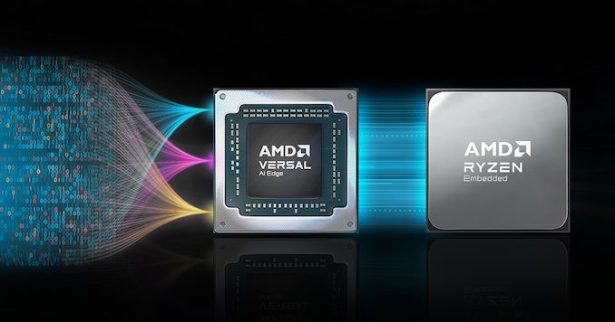
The Embedded+ architecture integrates the capabilities of their Ryzen Embedded processors with their Versal AI Edge adaptive SoCs onto one packaged board. AMD targets key areas that require good computational power and power efficiency. This synergy enables Embedded+ to handle AI inferencing and manage complex sensor data in real-time, which is crucial for applications in dynamic and demanding environments.
Giving ODMs the ability to have both Ryzen Embedded and their Versal SoCs onto a single board is particularly beneficial for industries requiring low-latency response times between hardware and software, including autonomous vehicles, diagnostic equipment in healthcare, and precision machinery in industrial automation. The AMD Embedded+ architecture can also support various workloads across different processor types, including x86 and ARM, along with AI engines and FPGA fabric, which offers flexibility and scalability of embedded computing solutions within industries.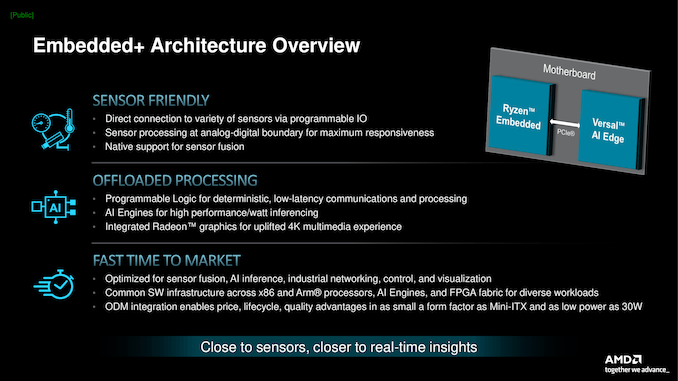
The Embedded+ platform from AMD offers plenty of compatibility with various sensor types and their corresponding interfaces. It facilitates direct connectivity with standard peripherals and industrial sensors through Ethernet, USB, and HDMI/DP interfaces. The AMD Ryzen Embedded processors within the architecture can handle inputs from traditional image sensors such as RGB, monochrome, and even advanced neuromorphic types while supporting industry-standard image sensor interfaces like MIPI and LVDS.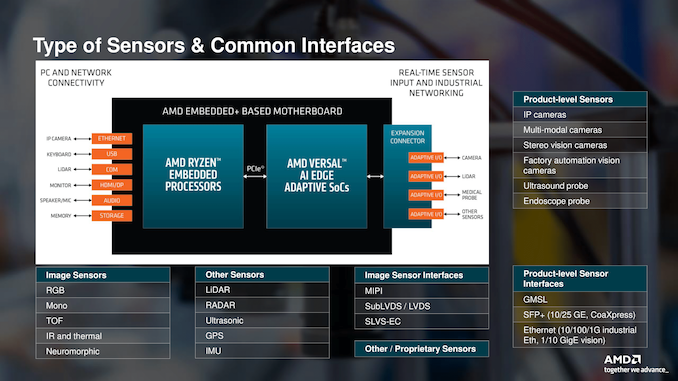
Further enhancing its capability, the AMD Versal AI Edge adaptive SoCs on the Embedded+ motherboard offer adaptable I/O options for real-time sensor input and industrial networking. This includes interfacing with LiDAR, RADAR, and other delicate and sophisticated sensors necessary for modern embedded systems in the industrial, medical, and automotive sectors. The platform's support for various product-level sensor interfaces, such as GMSL and Ethernet-based vision protocols, means it is designed and ready for integration into complex, sensor-driven systems.
AMD has also announced a new pre-integrated solution, which will be available for ODMs starting today. The Sapphire Technology VPR-4616-MB platform is a compact, Mini-ITX form factor motherboard that leverages the AMD Versal AI Edge 2302 SoC combined with an AMD Ryzen Embedded R2314 processor, which is based on Zen+ and has 4C/4T with 6 Radeon Vega compute units. It features a custom expansion connector for I/O boards, supporting a wide array of connectivity options, including dual DDR4 SO-DIMM slots with up to 64 GB capacity, one PCIe 3.0 x4 M.2 slot, and one SATA port for conventional HDDs and SSDs, The VPR-4616-MB also has a good array of networking capabilities including 2.5 Gb Ethernet and an M.2 Key E 2230 PCIe x1 slot for a wireless interface. It also supports the Linux-based Ubuntu 22.04 operating system.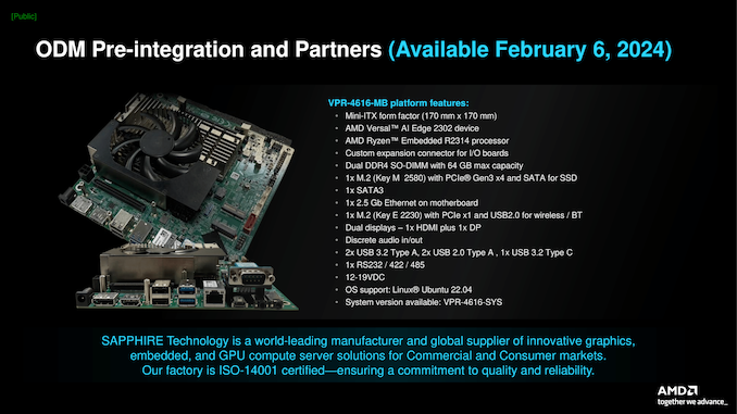
Also announced is a series of expansion boards that significantly broaden support for the Embedded+ architecture. The Octo GMSL Camera I/O board is particularly noteworthy for its ability to interface with multiple cameras simultaneously. It is undoubtedly suitable for high bandwidth vision-based systems, integral to sectors such as advanced driver-assistance systems (ADAS) and automated surveillance systems. These systems often require the integration of numerous image inputs for real-time processing and analysis, and the Octo GMSL board is engineered to meet this demand specifically.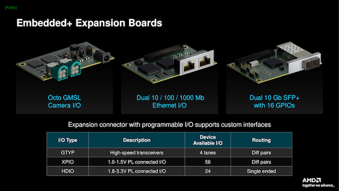
Additionally, a dual Ethernet I/O board is available, capable of supporting 10/100/1000 Mb connections, catering to environments that demand high-speed network communications. The Dual 10 Gb SFP+ board has 16 GPIOs for even higher bandwidth requirements, providing ample data transfer rates for tasks like real-time video streaming and large-scale sensor data aggregation. These expansion options broaden the scope of what the Embedded+ architecture is capable of in an edge and industrial scenario.
The Sapphire VPR-4616-MB is available for customers to purchase now and in a complete system configuration, including storage, memory, power supply, and chassis.
Gallery: AMD Embedded+ Architecture Slide Deck_thumb.png)
_thumb.png)
_thumb.png)
_thumb.png)
_thumb.png)
_thumb.png)
More...
-
02-06-24, 09:56 AM #12019
Anandtech: Sales of Client CPUs Soared in Q4 2023: Jon Peddie Research
Global client PC CPU shipments hit 66 million units in the fourth quarter of 2024, up both sequentially and year-over-year, a notable upturn in the PC processor market, according to the latest report from Jon Peddie Research. The data indicates that PC makers have depleted their CPU stocks and returned to purchases of processors from Intel during the quarter. This might also highlight that PC makers now have an optimistic business outlook.
AMD, Intel, and other suppliers shipped 66 million processors for client PCs during the fourth quarter of 2023, a 7% increase from the previous quarter (62 million) and a 22% rise from the year before (54 million). Despite a challenging global environment, the CPU market is showing signs of robust health.
70% of client PC CPUs sold in Q4 2023 were aimed at notebooks, which is up significantly from 63% represented by laptop CPUs in Q4 2022. Indeed, notebook PCs have been outselling desktop computers for years, so, unsurprisingly, the industry shipped more laptop-bound processors than desktop-bound CPUs. What is perhaps surprising is that the share of desktop CPUs in Q4 2022 shipments was 37%.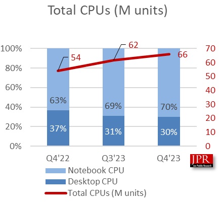
"Q4's increase in client CPU shipments from last quarter is positive news in what has been depressing news in general," said Jon Peddie, president of JPR. "The increase in upsetting news in the Middle East, combined with the ongoing war in Ukraine, the trade war with China, and the layoffs at many organizations, has been a torrent of bad news despite decreased inflation and increased GDP in the U.S. CPU shipments are showing continued gains and are a leading indicator."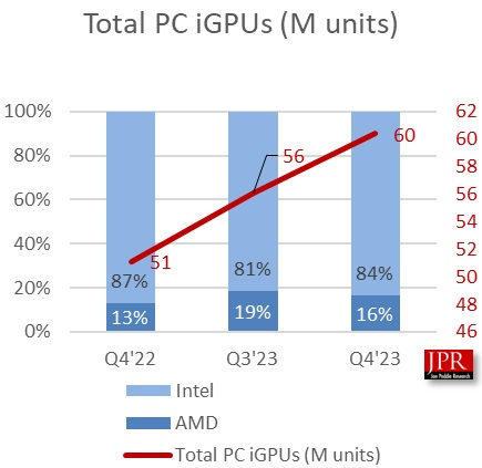
Meanwhile, integrated graphics processors (iGPUs) also grew, with shipments reaching 60 million units, up by 7% quarter-to-quarter and 18% year-over-year. Because the majority of client CPUs now feature a built-in GPU in one form or another, it is reasonable to expect shipments of iGPUs to grow along with shipments of client CPUs.
Jon Peddie Research predicts that iGPUs will dominate the PC segment, with their penetration expected to skyrocket to 98% within the next five years. This forecast may point to a future where integrated graphics become ubiquitous, though we would not expect discrete graphics cards to be extinct.
Meanwhile, the server CPU segment painted a different picture in Q4 2023, with a modest 2.8% growth from the previous quarter but a significant 26% decline year-over-year, according to JPR.
Despite these challenges, the overall positive momentum in the CPU market, as reported by Jon Peddie Research, suggests a sector that is adapting and thriving even amidst economic and geopolitical uncertainties.
More...
-
02-07-24, 02:01 AM #12020
Anandtech: TSMC to Build Second Fab in Japan: 6nm and 7nm Coming to Japan
Taiwan Semiconductor Manufacturing Co. on Tuesday formally announced plans to build a second fab in Japan. The fab will be run by Japan Advanced Semiconductor Manufacturing (JASM), a majority-owned TSMC subsidiary, and will make chips on 6 nm and 7 nm-class process technologies, which will make it the most advanced semiconductor production facility for logic chips in Japan.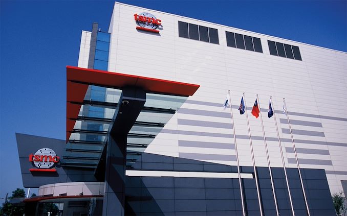
JASM is currently gearing up to start operating its first fab in Japan. This semiconductor production facility — set to be formally opened on February 24 — will be able to process up to 55,000 300-mm wafer starts per month (WSPM) using TSMC's 40 nm, 28 nm, 22 nm, 16 nm, and 12 nm-class process technologies. This fab is set to serve needs of JASM's minor investors, such as Sony, Toyota, and Denso, and other Japanese companies, such as automakers.
The new N6 and N7-capable fab will be located adjacent to JASM's upcoming fab in Kumamoto Prefecture, Japan. This facility will increase capacity of the site to over 100,000 300-mm wafer starts per month when it begins operations by the end of calendar 2027, according to TSMC. Capacity of the fab may be adjusted based on demand and other factors.
The initial Fab 23 that is coming online in the coming weeks or months was designed to address needs of Japanese companies like Sony and Toyota and ensure that they do not run into shortages of various commodity chips vital for their products yet not requiring advanced process technologies. The second fab, which is set to adopt 6 nm and 7 nm class process technologies will be able to produce considerably more sophisticated processors and will bring these production nodes for the first time in Japan. Essentially, the announcement of the new fab indicates that JASM is poised to slowly by surely catch up with TSMC's leading-edge fabs in Japan.
To build the new fab, owners of JASM will invest additional money in the venture and their total investments in the site will exceed $20 billion with 'strong support from the Japanese government,' TSMC said. As a result, JASM will be able to produce chips for a wide range of applications, including automotive, industrial, consumer and HPC-related applications.
Under the new investment agreement JASM's ownership will be divided as follows: TSMC will hold the largest stake at 86.5%, followed by SSS at 6.0%, DENSO at 5.5%, and Toyota at 2.0%.
More...


 Quote
Quote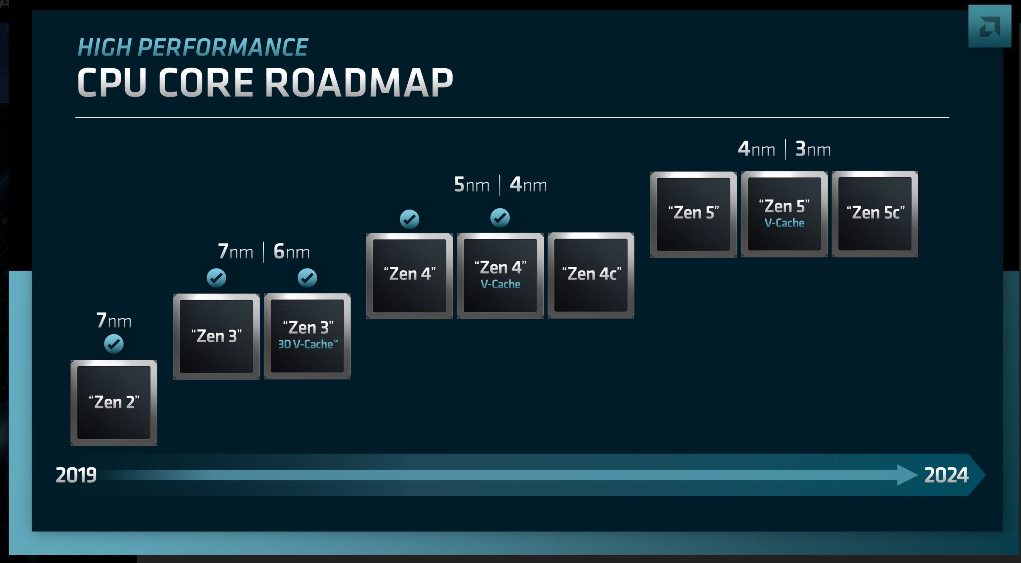
Thread Information
Users Browsing this Thread
There are currently 21 users browsing this thread. (0 members and 21 guests)


Bookmarks