

Results 12,031 to 12,040 of 12089
Thread: Anandtech News
-
02-20-24, 03:08 PM #12031
Anandtech: Capsule Review: AlphaCool Apex Stealth Metal 120mm Fan
Alphacool, a renowned name in the realm of PC cooling solutions, recently launched their Apex Stealth Metal series of cooling fans. Prior to their launch, the new fans had amassed a significant amount of hype in the PC community, in part because of the unfortunate misconception that the entire fan would be made out of metal.
Regardless of whether they're made entirely out of metal or not, however, these fans are notable for their unique construction, combining a metallic frame with plastic parts that are decoupled from the metal. This design choice not only contributes to the fan's aesthetic appeal but also plays a role in its operational efficiency.
The series includes two distinct models, the Apex Stealth Metal 120 mm and the Apex Stealth Metal Power 120 mm, distinguished primarily by their maximum rotational speeds. The former reaches up to 2000 RPM, while the latter, designed for more demanding applications, can achieve a remarkable 3000 RPM. Available in four color options – White, Matte Black, Chrome, and Gold – these fans offer a blend of style and functionality, making them a versatile choice for various PC builds.
More...
-
02-20-24, 03:08 PM #12032
Anandtech: Crucial T705 Gen5 NVMe SSD: A 14.5 GBps Consumer Flagship with 2400 MT/s 2
Crucial is unveiling the latest addition to its Gen5 consumer NVMe SSD lineup today - the T705 PCIe 5.0 M.2 2280 NVMe SSD. It takes over flagship duties from the Crucial T700 released last year. The company has been putting focus on the high-end consumer SSD segment in the last few quarters. The T700 was one of the first to offer more than 12 GBps read speeds, and the T705 being launched today is one of the first drives available for purchase in the 14+ GBps read speeds category.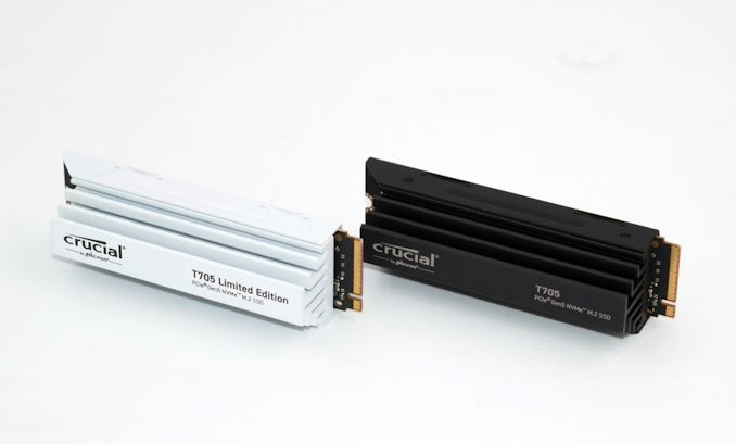
The Crucial T705 utilizes the same platform as the T700 from last year - Phison's E26 controller with Micron's B58R 232L 3D TLC NAND. The key difference is the B58R NAND operating at 2400 MT/s in the new T705 (compared to the 2000 MT/s in the T700). Micron's 232L NAND process has now matured enough for the company to put out 2400 MT/s versions with enough margins. Similar to the T700, this drive is targeted towards gamers, content creators, and professional users as well as data-heavy AI use-cases.
The move to 2400 MT/s NAND has allowed Crucial to claim an increase in the performance of the drive in all four corners - up to 20% faster random writes, and 18% higher sequential reads. Additionally, Crucial also claims more bandwidth in a similar power window for the new drive.
The T705 is launching in three capacities - 1TB, 2TB, and 4TB. Both heatsink and non-heatsink versions are available. Crucial is also offering a white heatsink limited edition for the 2TB version. This caters to users with white-themed motherboards that are increasingly gaining market presence.
Phison has been pushing DirectStorage optimizations in its high-end controllers, and it is no surprise that the T705 advertises the use of Phison's 'I/O+ Technology' to appeal to gamers. Given its high-performance nature, it is no surprise that the E26 controller needs to be equipped with DRAM for managing the flash translation layer (FTL). Crucial is using Micron LPDDR4 DRAM (1GB / TB of flash) in the T705 for this purpose.
Crucial is confident that the supplied passive heatsink is enough to keep the T705 from heavy throttling under extended use. The firmware throttling kicks in at 81C and protective shutdown at 90C. Flash pricing is not quite as low as it was last year, and the 2400 MT/s flash allows Micron / Crucial to place a premium on the product. At the 4TB capacity point, the drive can be purchased for as low as 18¢/GB, but the traditional 1TB and 2TB ones go for 20 - 26 ¢/GB depending on the heatsink option.Crucial T705 Gen5 NVMe SSD Specifications Capacity 1 TB 2 TB 4 TB Model Numbers CT1000T705SSD3 (Non-Heatsink)
CT1000T705SSD5 (Heatsink)CT2000T705SSD3 (Non-Heatsink)
CT2000T705SSD5 (Black Heatsink)
CT2000T705SSD5A (White Heatsink)CT4000T705SSD3 (Non-Heatsink)
CT4000T705SSD5 (Heatsink)Controller Phison PS5026-E26 NAND Flash Micron B58R 232L 3D TLC NAND at 2400 MT/s Form-Factor, Interface Double-Sided M.2-2280, PCIe 5.0 x4, NVMe 2.0 Sequential Read 13600 MB/s 14500 MB/s 14100 MB/s Sequential Write 10200 MB/s 12700 MB/s 12600 MB/s Random Read IOPS 1.4 M 1.55 M 1.5 M Random Write IOPS 1.75 M 1.8 M 1.8 M SLC Caching Dynamic (up to 11% of user capacity) TCG Opal Encryption Yes Warranty 5 years Write Endurance 600 TBW
0.33 DWPD1200 TBW
0.33 DWPD2400 TBW
0.33 DWPDMSRP $240 (24¢/GB) (Non- Heatsink)
$260 (26¢/GB) (Heatsink)$400 (20¢/GB) (Non- Heatsink)
$440 (22¢/GB) (Black Heatsink)
$484 (24.2¢/GB) (White Heatsink)$714 (17.85¢/GB) (Non- Heatsink)
$730 (18.25¢/GB) (Heatsink)
There are a number of Gen5 consumer SSDs slated to appear in the market over the next few months using the same 2400 MT/s B58R 3D TLC NAND and Phison's E26 controller (Sabrent's Rocket 5 is one such drive). The Crucial / Micron vertical integration on the NAND front may offer some advantage for the T705 when it comes to the pricing aspect against such SSDs. That said, the Gen5 consumer SSD market is still in its infancy with only one mass market (Phison E26) controller in the picture. The rise in consumer demand for these high-performance SSDs may coincide with other vendors such as Innogrit (with their IG5666) and Silicon Motion (with their SM2508) gaining traction. Currently, Crucial / Micron (with their Phison partnership) is the only Tier-1 vendor with a high-performance consumer Gen5 SSD portfolio, and the T705 cements their leadership position in the category further.
More...
-
02-21-24, 12:56 PM #12033
Anandtech: IFS Reborn as Intel Foundry: Expanded Foundry Business Adds 14A Process To
5 nodes in 4 years. This is what Intel CEO Pat Gelsinger promised Intel’s customers, investors, and the world at large back in 2021, when he laid out Intel’s ambitious plan to regain leadership in the foundry space. After losing Intel’s long-held spot as the top fab in the world thanks to compounding delays in the 2010s, the then-new Intel CEO bucked calls from investors to sell off Intel’s fabs, and instead go all-in on fabs like Intel has never done before, to become a top-to-bottom foundry service for the entire world to use.
Now a bit over two years later, and Intel is just starting to see the first fruits from that aggressive roadmap, both in terms of technologies and customers. Products based on Intel’s first EUV-based node, Intel 4, are available in the market today, and its high-volume counterpart, Intel 3, is ready as well. Meanwhile, Intel is putting the final touches on its first Gate-All-Around (GAAFET)/RibbonFET for 2024 and 2025. It’s a heady time for the company, but it’s also a critical one. Intel has reached the point where they need to deliver on those promises – and they need to do so in a very visible way.
To that end, today Intel’s Foundry group – the artist formally known as Intel Foundry Services – is holding its first conference, Direct Connect. And even more than being a showcase for customers and press, this is Intel’s coming-out party for the fab industry as a whole, where Intel’s foundry (and only Intel’s foundry) gets the spotlight, a rarity in the massive business that is Intel.
More...
-
02-21-24, 12:56 PM #12034
Anandtech: Arm Announces Neoverse V3 and N3 CPU Cores: Building Bigger and Moving Fas
A bit over 5 years ago, Arm announced their Neoverse initiative for server, cloud, and infrastructure CPU cores. Doubling-down on their efforts to break into the infrastructure CPU market in a big way, the company set about an ambitious multi-year plan to develop what would become a trio of CPU core lineups to address different segments of the market – ranging from the powerful V series to the petite E series core. And while things have gone a little differently than Arm initially projected, they’re hardly in a position to complain, as the Neoverse line of CPU cores has never been as successful as it is now. Custom CPU designs based on Neoverse cores are all the rage with cloud providers, and the broader infrastructure market has seen its own surge.
Now, as the company and its customers turn towards 2024 and a compute market that is in the throes of another transformative change due to insatiable demand for AI hardware, Arm is preparing to release its next generation of Neoverse CPU core designs to its customers. And in the process, the company is reaching the culmination of the original Neoverse roadmap.
This morning the company is taking the wraps off of the V3 CPU architecture (codename Poseidon) for high-performance systems, as well as the N3 CPU architecture (codename Hermes) for balanced systems. These designs are now ready for customers to begin integrating into their own chip designs, with both the individual CPU core designs as well as the larger Neoverse Compute Subsystems (CSS) available. Between the various combinations of IP configurations, Arm is looking to offer something for everyone, and especially chip designers who are looking to integrate ready-made IP for a quick turnaround in developing their own chips.
With that said, it should be noted that today’s announcement is also a lighter one than what we’ve come to expect from previous Neoverse announcements. Arm isn’t releasing any of the deep architectural details on the new Neoverse platforms today, so while we have the high-level details on the hardware and some basic performance estimates, the underlying details on the CPU cores and their related plumbing is something Arm is keeping to themselves until a later time.
More...
-
02-22-24, 12:00 PM #12035
Anandtech: Arm and Samsung to Co-Develop 2nm GAA-Optimized Cortex Cores
Arm and Samsung this week announced their joint design-technology co-optimization (DTCO) program for Arm's next-generation Cortex general-purpose CPU cores as well as Samsung's next-generation process technology featuring gate-all-around (GAA) multi-bridge-channel field-effect transistors (MBCFETs).
"Optimizing Cortex-X and Cortex-A processors on the latest Samsung process node underscores our shared vision to redefine what’s possible in mobile computing, and we look forward to continuing to push boundaries to meet the relentless performance and efficiency demands of the AI era," said Chris Bergey, SVP and GM, Client Business at Arm.
Under the program, the companies aim to deliver tailored versions of Cortex-A and Cortex-X cores made on Samsung's 2 nm-class process technology for various applications, including smartphones, datacenters, infrastructure, and various customized system-on-chips. For now, the companies does not say whether they aim to co-optimize Arm's Cortex cores for Samsung's 1st generation 2 nm production node called SF2 (due in 2025), or the plan is to optimize these cores for all SF2-series technologies, including SF2 and SF2P.
GAA nanosheet transistors with channels that are surrounded by gates on all four sides have a lot of options for optimization. For example, nanosheet channels can be widened to increase drive current and boost performance or shrunken to reduce power consumption and cost. Depending on the application, Arm and Samsung will have plenty of design choices.
Keeping in mind that we are talking about Cortex-A cores aimed at a wide variety of applications as well as Cortex-X cores designed specifically to deliver maximum performance, the results of the collaborative work promise to be quite decent. In particular, we are looking forward Cortex-X cores with maximized performance, Cortex-A cores with optimized performance and power consumption, and Cortex-A cores with reduced power consumption.
Nowadays collaboration between IP (intellectual property) developers, such as Arm, and foundries, such as Samsung Foundry, is essential to maximize performance, reduce power consumption, and optimize transistor density. The joint work with Arm will ensure that Samsung's foundry partners will have access to processor cores that can deliver exactly what they need.
More...
-
02-23-24, 01:07 AM #12036
Anandtech: AMD CEO Dr. Lisa Su to Deliver Opening Keynote at Computex 2024
Taiwan External Trade Development Council (TAITRA), the organizer of Computex, announced today that Dr. Lisa Su, AMD's chief executive officer, will give the trade show's Opening Keynote. Su's speech is set for the morning of June 3, 2024, shortly before the formal start of the show. According to AMD, the keynote talk will be "highlighting the next generation of AMD products enabling new experiences and breakthrough AI capabilities from the cloud to the edge, PCs and intelligent end devices."
This year's Computex is focused on six key areas: AI computing, Advanced Connectivity, Future Mobility, Immersive Reality, Sustainability, and Innovations. Being a leading developer of CPUs, AI and HPC GPUs, consumer GPUs, and DPUs, AMD can talk most of these topics quite applicably.
As AMD is already mid-cycle on most of their product architectures, the company's most recent public roadmaps have them set to deliver major new CPU and GPU architectures before the end of 2024 with Zen 5 CPUs and RDNA 4 GPUs, respectively. AMD has not previously given any finer guidance on when in the year to expect this hardware, though AMD's overall plans for 2024 are notably more aggressive than the start of their last architecture cycle in 2022. Of note, the company has previously indicated that it intends to launch all 3 flavors of the Zen 5 architecture this year – not just the basic core, but also Zen 5c and Zen 5 with V-Cache – as well as a new mobile SoC (Strix Point). By comparison, it took AMD well into 2023 to do the same with Zen 4 after starting with a fall 2022 launch for those first products.
This upcoming keynote will be Lisa Su's third Computex keynote after her speeches at Computex 2019 and Computex 2022. In both cases she also announced upcoming AMD products.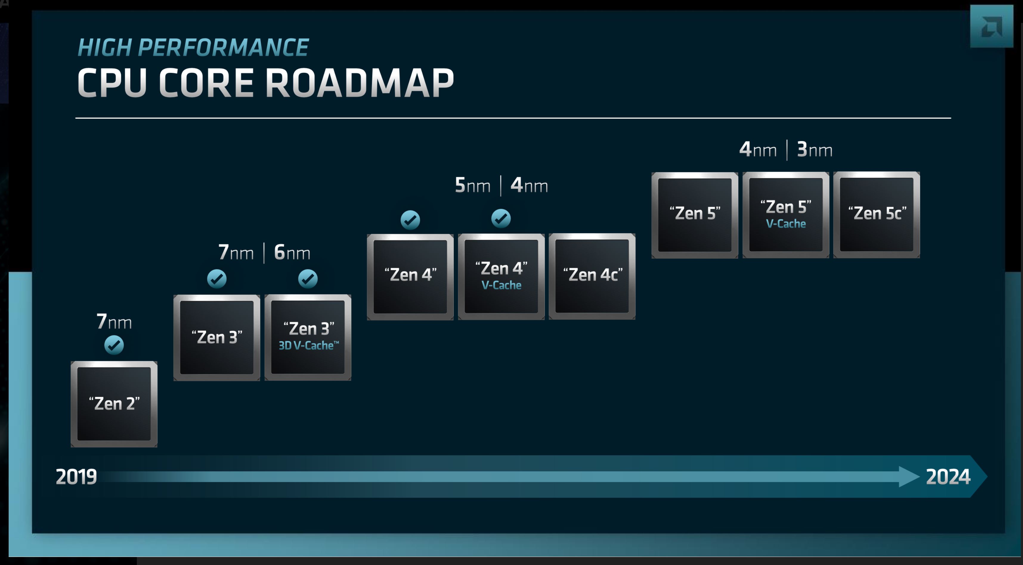
AMD 2022 Financial Analyst Day CPU Core Roadmap
In 2019, she showcased performance improvements of then upcoming 3rd Generation Ryzen desktop processors and 7nm EPYC datacenter processors. Lisa Su also highlighted AMD's advancements in 7nm process technology, showcasing the world's first 7nm gaming GPU, the Radeon VII, and the first 7nm datacenter GPU, the Radeon Instinct MI60.
In 2022, the head of AMD offered a sneak peek at the then-upcoming Ryzen 7000-series desktop processors based on the Zen 4 architecture, promising significant performance improvements. She also teased the next generation of Radeon RX 7000-series GPUs with the RDNA 3 architecture.
More...
-
02-23-24, 09:34 AM #12037
Anandtech: AMD Fixed the STAPM Throttling Issue, So We Retested The Ryzen 7 8700G and
When we initially reviewed the latest Ryzen 8000G APUs from AMD last month, the Ryzen 7 8700G and Ryzen 5 8600G, we became aware of an issue that caused the APUs to throttle after a few minutes. This posed an issue for a couple of reasons, the first being it compromised our data to reflect the true capabilities of the processors, and the second, it highlighted an issue that AMD forgot to disable from their mobile series of Pheonix chips (Ryzen 7040) when implementing it over to the desktop.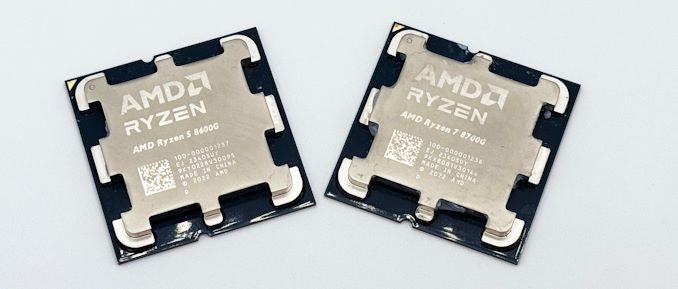
We updated the data in our review of the Ryzen 7 8700G and Ryzen 5 8600G to reflect performance with STAPM on the initial firmware and with STAPM removed with the latest firmware. Our updated and full review can be accessed by clicking the link below:
As we highlighted in our Ryzen 8000G APU STAPM Throttling article, AMD, through AM5 motherboard vendors such as ASUS, has implemented updated firmware that removes the STAPM limitation. Just to quickly recap the Skin Temperature-Aware Power Management (STAPM) feature and what it does, AMD introduced it in 2014. STAPM itself is a feature implemented into their mobile processors. It is designed to extend the on-die power management by considering the processor's internal temperatures taken by on-chip thermal diodes and the laptop's surface temperature (i.e., the skin temperature).
The aim of STAPM is to prevent laptops from becoming uncomfortably warm for users, allowing the processor to actively throttle back its heat generation based on the thermal parameters between the chassis and the processor itself. The fundamental issue with STAPM in the case of the Ryzen 8000G APUs, including the Ryzen 7 8700G and Ryzen 5 8600G, is that these are mobile processors packaged into a format for use with the AM5 desktop platform. As a desktop platform is built into a chassis that isn't placed on a user's lap, the STAPM feature becomes irrelevant.
As we saw when we ran a gaming load over a prolonged period of time on the Ryzen 7 8700G with the firmware available at launch, we hit power throttling (STAPM) after around 3 minutes. As we can see in the above chart, power dropped from a sustained value of 83-84 W down to around 65 W, representing a drop in power of around 22%. While we know Zen 4 is a very efficient architecture at lower power values, overall performance will drop once this limit is hit. Unfortunately, AMD forgot to remove STAPM limits when transitioning Pheonix to the AM5 platform.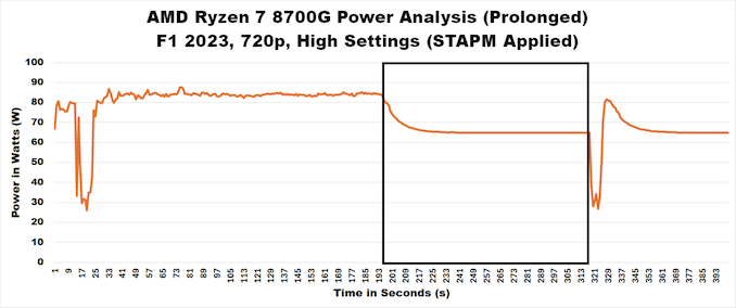
Retesting the same game (F1 2023) at the same settings (720p High) with the firmware highlighting that STAPM had been removed, we can see that we aren't experiencing any of the power throttling we initially saw. We can see power is sustained for over 10 minutes of testing (we did test for double this), and we saw no drops in package power, at least not from anything related to STAPM. This means for users on the latest firmware on whatever AM5 motherboard is being used, power and, ultimately, performance remain consistent with what the Ryzen 7 8700G should have been getting at launch.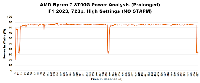
The key question is, does removing the STAPM impact our initial results in our review of the Ryzen 7 8700G and Ryzen 5 8600G? And if so, by how much, or if at all? We added the new data to our review of the Ryzen 7 8700G and Ryzen 5 8600G but kept the initial results so that users can see if there are any differences in performance. Ultimately, benchmark runs are limited to the time it takes to run them, but in real-world scenarios, tasks such as video rendering and longer sustained loads are more likely to show gains in performance. After all, a drop of 22% in power is considerable, especially over a task that could take an hour.
Using one of our longer benchmarks, such as Blender 3.6, to highlight where performance gains are notable when using the latest firmware with the STAPM limitations removed, we saw an increase in performance of around 7.5% on the Ryzen 7 8700G with this removed. In the same benchmark, we saw an increase of around 4% on the Ryzen 5 8600G APU.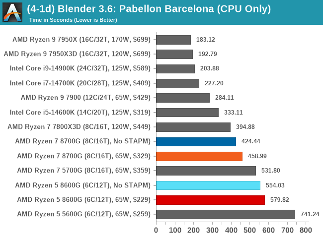
Over all of the Blender 3.6 tests in the rendering section of our CPU performance suite, performance gains hovered between 2 and 4.4% on the Ryzen 5 8600G, and between 5 and 7.5% on the Ryzen 8700G, which isn't really free performance, it's the performance that should have been there to begin with at launch.
Looking at how STAPM affected our initial data, we can see that the difference in World of Tanks at 768p Minumum settings had a marginal effect at best through STAPM by around 1%. Given how CPU-intensive World of Tanks is, and combining this with integrated graphics, the AMD Ryzen APUs (5000G and 8000G) both shine compared to Intel's integrated UHD graphics in gaming. Given that gaming benchmarks are typically time-limited runs, it's harder to identify performance gains. The key to takeaway here is that with the STAPM limitation removed, the performance shouldn't drop over sustained periods of time, so our figures above and our updated review data aren't compromised.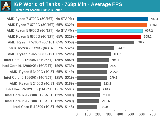
Regarding gaming with a discrete graphics card, we saw no drastic changes in performance, as highlighted by our Total War Warhammer 3 at 1440p Ultra benchmark. Across the board, in our discrete graphics results with both the Ryzen 7 8700G and the Ryzen 5 8600G, we saw nothing but marginal differences in performance (less than 1%). As we've mentioned, removing the STAPM limitations doesn't necessarily improve performance. Still, it allows the APUs to keep the same performance level for sustained periods, which is how it should have been at launch. With STAPM applied as with the initial firmware at launch on AM5 motherboards, power would drop by around 22%, limiting the full performance capability over prolonged periods.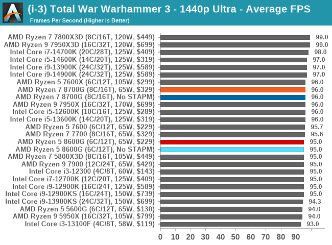
As we've mentioned, we have updated our full review of the AMD Ryzen 7 8700G and Ryzen 5 8600G APUs to reflect our latest data gathered from testing on the latest firmware. Still, we can fully confirm that the STAPM issue has been fixed and that the performance is as it should be on both chips.
You can access all of our updated data in our review of the Ryzen 7 8700G and Ryzen 5 8600G by clicking the link below.
More...
-
02-26-24, 09:28 AM #12038
Anandtech: Intel Previews Sierra Forest with 288 E-Cores, Announces Granite Rapids-D
At MWC 2024, Intel confirmed that Granite Rapids-D, the successor to Ice Lake-D processors, will come to market sometime in 2025. Furthermore, Intel also provided an update on the 6th Gen Xeon Family, codenamed Sierra Forest, which is set to launch later this year and will feature up to 288 cores designed for vRAN network operators to improve performance in boost per rack for 5G workloads.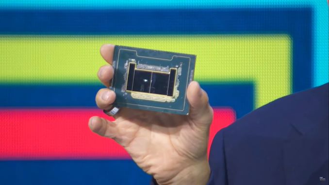
These chips are designed for handling infrastructure, applications, and AI workloads and aim to capitalize on current and future AI and automation opportunities, enhancing operational efficiency and ownership costs in next-gen applications and reflecting Intel's vision of integrating 'AI Everywhere' across various infrastructures.
Intel Sierra Forest: Up to 288 Efficiency Cores, Set for 2H 2024
The first of Intel's announcements at MWC 2024 focuses on their upcoming Sierra Forest platform, which is scheduled for the 2nd half of 2024. Initially announced in February 2022 during Intel's Investor Meeting, Intel is splitting its server roadmap into solutions featuring only performance (P) and efficiency (E) cores. We already know that Sierra Forest's new chips feature a full E-core architecture designed for maximum efficiency in scale-out, cloud-native, and contained environments.
These chips utilize CPU chiplets built on the Intel 3 process alongside twin I/O chiplets based on the Intel 7 node. This combination allows for a scalable architecture, which can accommodate increasing core counts by adding more chiplets, optimizing performance for complex computing environments.
Intel's Sierra Forest, Intel's full E-core designed Xeon processor family, is anticipated to significantly enhance power efficiency with up to 288 E-cores per socket. Intel also claims that Sierra Forest is expected to deliver 2.7 times the performance-per-rack compared to an unspecified platform from 2021; this could be either Ice Lake or Cascade Lake, but Intel didn't mention which.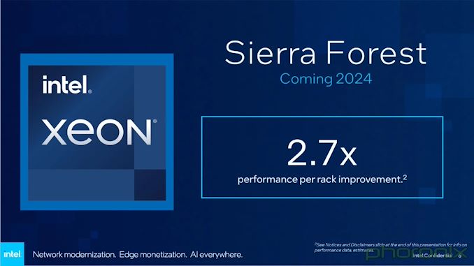
Additionally, Intel is promising savings of up to 30% in Infrastructure Power Management with Sierra Forest as their Infrastructure Power Manager (IPM) application is now available commercially for 5G cores. Power manageability and efficiency are growing challenges for network operators, so IPM is designed to allow network operators to optimize energy efficiency and TCO savings.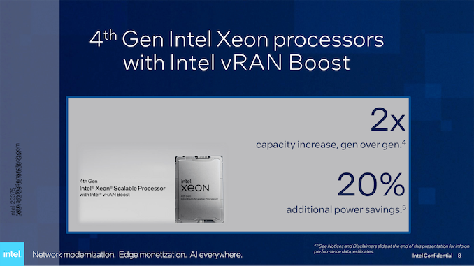
Intel also includes vRAN, which is vital for modern mobile networks, and many operators are forgoing opting for specific hardware and instead leaning towards virtualized radio access networks (vRANs). Using vRAM Boost, which is an integrated accelerator within Xeon Processors, Intel states that the 4th Gen Xeon should be able to reduce power consumption by around 20% while doubling the available network capacity.
Intel's push for 'AI Everywhere' is also a constant focus here, with AI's role in vRAM management becoming more crucial. Intel has announced the vRAM AI Developer Kit, which is available to select partners. This allows partners and 5G network providers to develop AI models to optimize for vRAM applications, tailor their vRAN-based functions to more use cases, and adapt to changes within those scenarios.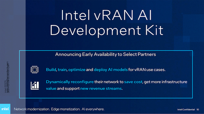
Intel Granite Rapids-D: Coming in 2025 For Edge Solutions
Intel's Granite Rapids-D, designed for Edge solutions, is set to bolster Intel's role in virtual radio access network (vRAN) workloads in 2025. Intel also promises marked efficiency enhancements and some vRAN Boost optimizations similar to those expected on Sierra Forest. Set to follow on from the current Ice Lake-D for the edge; Intel is expected to use the performance (P) cores used within Granite Rapids server parts and optimize the V/F curve designed for the lower-powered Edge platform. As outlined by Intel, the previous 4th generation Xeon platform effectively doubled vRAN capacity, enhancing network capabilities while reducing power consumption by up to 20%.
Granite Rapids-D aims to further these advancements, utilizing Intel AVX for vRAN and integrated Intel vRAN Boost acceleration, thereby offering substantial cost and performance benefits on a global scale. While Intel hasn't provided a specific date (or month) of when we can expect to see Granite Rapids-D in 2025, Intel is currently in the process of sampling these next-gen Xeon-D processors with partners, aiming to ensure a market-ready platform at launch.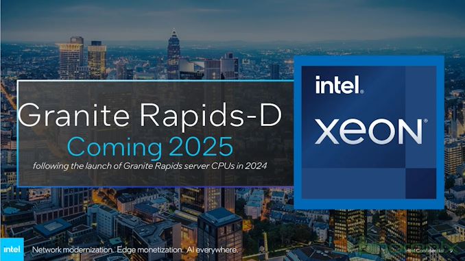
Gallery: Intel Sierra Forest and Granite Rapids-D Slide Deck MWC 2024


Related Reading- Hot Chips 2023: Intel Details More on Granite Rapids and Sierra Forest Xeons
- Intel Updates Data Center Roadmap: Xeons on Track - Emerald in Q4'23, Sierra Forest in H1'24
- IFS Reborn as Intel Foundry: Expanded Foundry Business Adds 14A Process to Roadmap
More...
-
02-26-24, 10:25 PM #12039
Anandtech: Micron Kicks Off Production of HBM3E Memory
Micron Technology on Monday said that it had initiated volume production of its HBM3E memory. The company's HBM3E known good stack dies (KGSDs) will be used for Nvidia's H200 compute GPU for artificial intelligence (AI) and high-performance computing (HPC) applications, which will ship in the second quarter of 2024.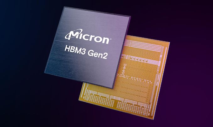
Micron has announced it is mass-producing 24 GB 8-Hi HBM3E devices with a data transfer rate of 9.2 GT/s and a peak memory bandwidth of over 1.2 TB/s per device. Compared to HBM3, HBM3E increases data transfer rate and peak memory bandwidth by a whopping 44%, which is particularly important for bandwidth-hungry processors like Nvidia's H200.
Nvidia's H200 product relies on the Hopper architecture and offers the same computing performance as the H100. Meanwhile, it is equipped with 141 GB of HBM3E memory featuring bandwidth of up to 4.8 TB/s, a significant upgrade from 80 GB of HBM3 and up to 3.35 TB/s bandwidth in the case of the H100.
Micron's memory roadmap for AI is further solidified with the upcoming release of a 36 GB 12-Hi HBM3E product in March 2024. Meanwhile, it remains to be seen where those devices will be used.
Micron uses its 1β (1-beta) process technology to produce its HBM3E, which is a significant achievement for the company as it uses its latest production node for its data center-grade products, which is a testament to the manufacturing technology.
Starting mass production of HBM3E memory ahead of competitors SK Hynix and Samsung is a significant achievement for Micron, which currently holds a 10% market share in the HBM sector. This move is crucial for the company, as it allows Micron to introduce a premium product earlier than its rivals, potentially increasing its revenue and profit margins while gaining a larger market share.
"Micron is delivering a trifecta with this HBM3E milestone: time-to-market leadership, best-in-class industry performance, and a differentiated power efficiency profile," said Sumit Sadana, executive vice president and chief business officer at Micron Technology. "AI workloads are heavily reliant on memory bandwidth and capacity, and Micron is very well-positioned to support the significant AI growth ahead through our industry-leading HBM3E and HBM4 roadmap, as well as our full portfolio of DRAM and NAND solutions for AI applications."
Source: Micron
More...
-
02-27-24, 09:24 AM #12040
Anandtech: Samsung Launches 12-Hi 36GB HBM3E Memory Stacks with 10 GT/s Speed
Samsung announced late on Monday the completion of the development of its 12-Hi 36 GB HBM3E memory stacks, just hours after Micron said it had kicked off mass production of its 8-Hi 24 GB HBM3E memory products. The new memory packages, codenamed Shinebolt, increase peak bandwidth and capacity compared to their predecessors, codenamed Icebolt, by over 50% and are currently the world's fastest memory devices.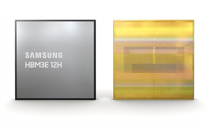
As the description suggests, Samsung's Shinebolt 12-Hi 36 GB HBM3E stacks pack 12 24Gb memory devices on top of a logic die featuring a 1024-bit interface. The new 36 GB HBM3E memory modules feature a data transfer rate of 10 GT/s and thus offer a peak bandwidth of 1.28 GB/s per stack, the industry's highest per-device (or rather per-module) memory bandwidth.
Meanwhile, keep in mind that developers of HBM-supporting processors tend to be cautious, so they will use Samsung's HBM3E at much lower data transfer rates to some degree because of power consumption and to some degree to ensure ultimate stability for artificial intelligence (AI) and high-performance computing (HPC) applications.
To make its Shinebolt 12-Hi 36 GB HBM3E memory stacks, Samsung had to use several advanced technologies. First, the 36 GB HBM3E memory products are based on memory devices made on Samsung's 4th generation 10nm-class (14nm) fabrication technology, which is called and uses extreme ultraviolet (EUV) lithography.Samsung HBM Memory Generations HBM3E
(Shinebolt)HBM3
(Icebolt)HBM2E
(Flashbolt)HBM2
(Aquabolt)Max Capacity 36GB 24 GB 16 GB 8 GB Max Bandwidth Per Pin 9.8 Gb/s 6.4 Gb/s 3.6 Gb/s 2.0 Gb/s Number of DRAM ICs per Stack 12 12 8 8 Effective Bus Width 1024-bit Voltage ? 1.1 V 1.2 V 1.2 V Bandwidth per Stack 1.225 TB/s 819.2 GB/s 460.8 GB/s 256 GB/s
Secondly, to ensure that 12-Hi HBM3E stacks have the same z-height as 8-Hi HBM3 products, Samsung used its advanced thermal compression non-conductive film (TC NCF), which allowed it to achieve the industry's smallest gap between memory devices at seven micrometers (7 µm). By shrinking gaps between DRAMs, Samsung increases vertical density and mitigates chip die warping. Furthermore, Samsung uses bumps of various sizes between the DRAM ICs; smaller bumps are used in areas for signaling. In contrast, larger ones are placed in spots that require heat dissipation, which improves thermal management.
Samsung estimates that its 12-Hi HBM3E 36 GB modules can increase the average speed for AI training by 34% and expand the number of simultaneous users of inference services by more than 11.5 times. However, the company has not elaborated on the size of the LLM.
Samsung has already begun providing samples of the HBM3E 12H to customers, with mass production scheduled to commence in the first half of this year.
Source: Samsung
More...


 Quote
QuoteThread Information
Users Browsing this Thread
There are currently 10 users browsing this thread. (0 members and 10 guests)


Bookmarks