

Results 12,051 to 12,060 of 12089
Thread: Anandtech News
-
03-07-24, 04:25 PM #12051
Anandtech: V-Color Has New RDIMM Octo-Kits For Threadripper 7000 CPUs: 768 GB Kits St
V-Color has launched several EXPO-certified DDR5 RDIMM memory kits for AMD's Ryzen Threadripper 7000 Pro and non-Pro platforms. The new RDIMM memory kits, which only come in an eight-DIMM configuration, will enable workstation users to push the limits on the WRX90 platform with frequencies up to DDR5-7200 and memory kit capacities up to a staggering 768 GB (8 x 96 GB).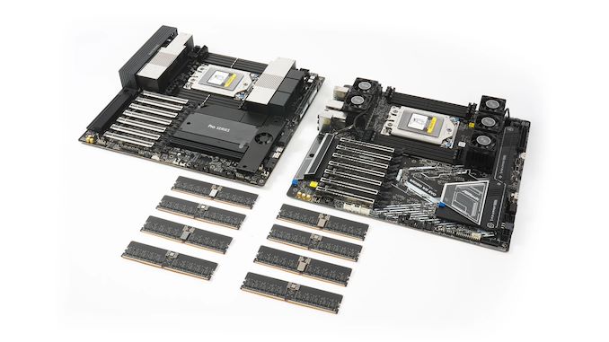
These are your typical run-of-the-mill modules without the fancy heatsinks and flashy RGB lighting. The recipe for the RDIMMs revolves around a 10-layer PCB paired with SK hynix's DRAM chips. And as the Threadripper platforms are all one DIMM per channel (1DPC) designs, V-Color's octo-kits are intended to populate all the memory slots on the WRX90 motherboard in one go.
V-Color is offering their RDIMM kits in several capacities and frequencies, with kit capacities ranging from 128 GB (8 x 16 GB) up to 768 GB (8 x 96 GB), while clockspeeds start at DDR5-5600 and top out at DDR5-7200.
Typical for RDIMM kits, the maximum frequency will vary depending on the memory kit capacity. There are two factors to consider: binning costs and achieving stability at faster frequencies on higher capacities is more challenging for the processor. Ryzen Threadripper 7000 Pro and non-Pro chips officially support DDR5-5200 memory modules. Anything higher is overclocking; stability depends on the processor's integrated memory controller (IMC) quality. DDR5-7200 is only available on V-Color's 128 GB, 192 GB, and 256 GB memory kits. Meanwhile, the 512 GB and 768 GB memory kits top out at DDR5-6000.
The DDR5-5600 and DDR5-6000 memory kits are the only ones rated to run at a relatively modest 1.25 V. The higher-end ones require 1.40 V due to the higher frequency and tighter memory timings. The memory timings on V-Color's RDIMM memory kits are decent, though they're far from rivaling premium DDR5 mainstream memory kits. The DDR5-5600 memory kit has 36-38-38-38-80 timings, whereas the DDR5-6000 and DDR5-6400 memory flaunts flaunt 32-39-39-102 timings. At the same time, V-Color binned the DDR5-6600 and DDR5-6800 memory kits for 34-46-46-92 and the DDR5-7000 and DDR5-7200 memory kits for 34-43-43-102 and 36-46-46-112, respectively.V-Color DDR5 RDIMM Octo-Kit Specifications Memory Kit Capacity Configuration Frequency CAS Latency Voltage Price 768 GB 8 x 96 GB DDR5-5600 - DDR5-6000 CL 36 1.25 V $4,839.99 - $4,919.99 512 GB 8 x 64 GB DDR5-5600 - DDR5-6000 CL 36 1.25 V $3,429.99 - $3,509.99 384 GB 8 x 48 GB DDR5-6400 - DDR5-6800 CL 32 - CL 34 1.40 V $3,339.99 - $3,559.99 256 GB 8 x 32 GB DDR5-5600 - DDR5-7200 CL 32 - CL 36 1.25 V - 1.40 V $2,139.99 - $3,479.99 192 GB 8 x 24 GB DDR5-5600 - DDR5-7200 CL 32 - CL 36 1.25 V - 1.40 V $1,579.99 - $2,199.99 128 GB 8 x 16 GB DDR5-5600 - DDR5-7200 CL 32 - CL 36 1.25 V - 1.40 V $1,049.99 - $1,669.99
V-Color's RDIMM products are overclocked memory kits with a limited lifetime warranty. They come with AMD EXPO support to facilitate one-click memory overclocking. The memory kits are built specifically for the WRX90 platform but should work on Intel platforms (your mileage will vary, of course). Regarding the QVL, V-Color has validated the brand's overclocked RDIMMs on the Asus Pro WS WRX90E-Sage SE and the ASRock WRX90 WS Evo, motherboards that cost over $1,000.
The 128 GB DDR5-5600 memory kit is the most affordable out of the lot, with an MSRP of $1,049.99, whereas the 192 GB counterpart sells for $1,579.99. At the other end of the spectrum, the flagship 768 GB DDR5-6000 memory kit has an hefty $4,919.99 price tag. V-Color's RDIMM memory kits are up for pre-order on the company's online store, and the vendor will ship orders on March 15. The memory kits will be available worldwide through official distribution partners on the same date.
More...
-
03-07-24, 07:17 PM #12052
Anandtech: Variable Refresh Rate Support Comes to NVIDIAs GeForce Now Cloud Streamin
Today NVIDIA has brought variable refresh rate support to its GeForce Now cloud gaming service. The company initially promised variable refresh support on GeForce Now back in early January during CES, and has seemingly waited so that it could launch alongside GeForce Now Day Passes, which are also now available.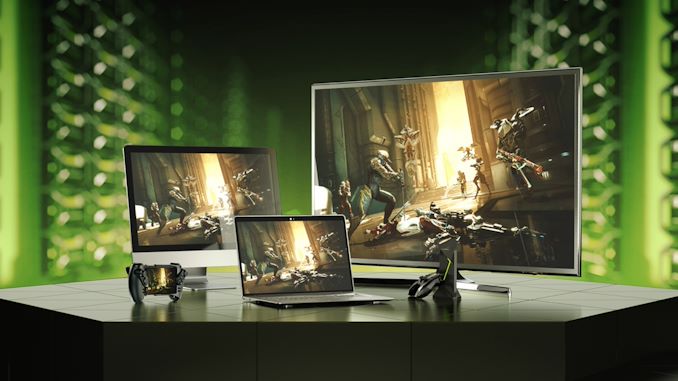
Variable refresh rate (VRR) technologies, including NVIDIA's own G-Sync, have been around for around a decade now, and allow a monitor to synchronize its refresh rate to the instantaneous framerate of a game. This synchronization prevents screen tearing, when two or more frames are present on a display at the same time. Without a VRR technology, gamers either have to tolerate the visual incongruity of screen tearing or enable V-Sync, which solves screen tearing by locking the framerate to the refresh rate (or a fraction thereof). VRR became popular because V-Sync added latency and could depress framerates due to it effectively being a framerate limiter.
Dubbed "Cloud G-Sync", NVIDIA touts not only a screen tearing-free experience for GeForce Now thanks to variable refresh rate support, but also lower latency thanks to “varying the stream rate to the client, driving down total latency on Reflex-enabled games.” Prior to VRR’s debut on GeForce Now, users either had to enable V-Sync in-game, enable a stream-level V-Sync setting that had the benefit of not locking the game framerate, or accept screen tearing. GeForce Now Ultimate members will also be able to pair VRR with Reflex-powered 60 FPS and 120 FPS streaming modes.
According to NVIDIA’s technical documentation, variable refresh rate support on GeForce Now can work with both Mac and Windows PCs hooked up to a VRR-capable monitor. This includes G-Sync monitors on Windows, as well as VESA AdaptiveSync/FreeSync monitors, HDMI 2.1 VRR displays, and even Apple ProMotion displays, such as the panels built into their recent MacBook Pro laptops. The biggest compatibility hurdle at this time is actually on the GPU side of matters; Windows machines need an NVIDIA GPU to use VRR with GeForce Now. Intel and AMD GPUs are "not supported at this time."
Although G-SYNC originally came out in 2013 and GeForce Now has been available since 2015, the two never intersected until now. It’s not clear why NVIDIA waited so long to bring G-Sync to GeForce Now; the company’s original announcement merely states “newly improved cloud G-SYNC technology goes even further,” implying that it wasn’t possible before but doesn’t exactly explain why.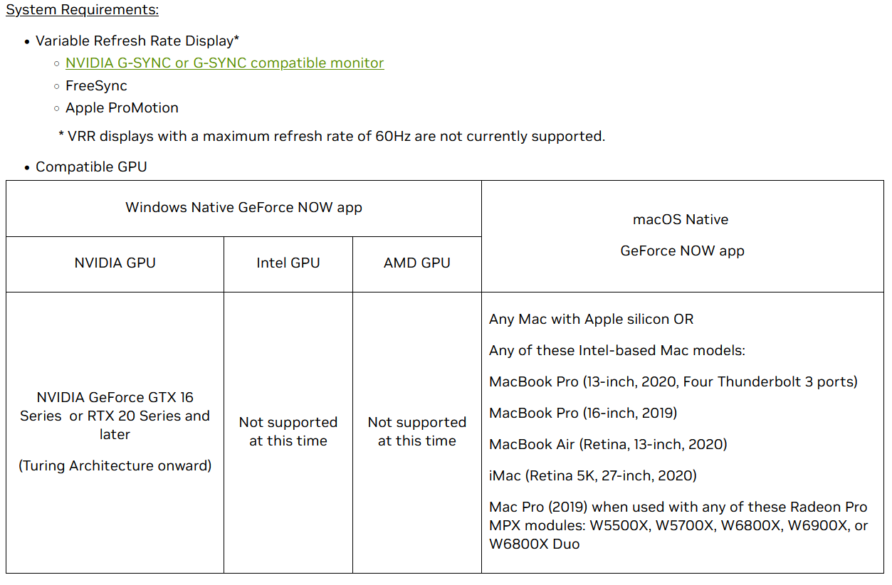
More...
-
03-08-24, 06:38 AM #12053
Anandtech: Intel CEO Pat Gelsinger to Deliver Computex Keynote, Showcasing Next-Gen P
Taiwan External Trade Development Council (TAITRA), the organizer of Computex, has announced that Pat Gelsinger, chief executive of Intel, will deliver a keynote at Computex 2024 on June 4, 2024. Focusing on the trade show's theme of artificial intelligence, he will showcase Intel's next-generation AI-enhanced products for client and datacenter computers.
According to TAITRA's press release, Pat Gelsinger will discuss how Intel's product lineup, including the AI-accelerated Intel Xeon, Intel Gaudi, and Intel Core Ultra processor families, opens up new opportunities for client PCs, cloud computing, datacenters, and network and edge applications. He will also discuss superior performance-per-watt and lower cost of ownership of Intel's Xeon processors, which enhance server capacity for AI workloads.
The most intriguing part of Intel's Computex keynote will of course be the company's next-generation AI-enhanced products for client and datacenter computers. At this point Intel is prepping numerous products that pose a lot of interest, including the following:
- Arrow Lake and Lunar Lake processors made on next-generation process technologies for desktop and mobile PCs and featuring all-new microarchitectures;
- Granite Rapids CPUs for datacenters based on a high-performance microarchitecture;
- Sierra Forest processors with up to 288 cores for cloud workloads based on codenamed Crestmont energy-efficient cores;
- Gaudi 3 processors for AI workloads that promise to quadruple BF16 performance compared to Gaudi 2.
- Battlemage graphics processing units.
All of these products are due to be released in 2024-2025, so Intel could well demonstrate them and showcase their performance advantages, or even formally launch some of them, at Computex. What remains to be seen is whether Intel will also give a glimpse at products that are further away, such as Clearwater Shores and Falcon Shores.
More...
-
03-08-24, 09:16 AM #12054
Anandtech: Marvell's 2nm IP Platform Enables Custom Silicon for Datacenters
Marvell this week introduced its new IP technology platform specifically tailored for custom chips for accelerated infrastructure made on TSMC's 2nm-class process technologies (possibly including N2 and N2P). The platform includes technologies essential for developing cloud-optimized accelerators, Ethernet switches, and digital signal processors.
"The 2nm platform will enable Marvell to deliver highly differentiated analog, mixed-signal, and foundational IP to build accelerated infrastructure," said Sandeep Bharathi, chief development officer at Marvell. "Our partnership with TSMC on our 5nm, 3nm and now 2nm platforms has been instrumental in helping Marvell expand the boundaries of what can be achieved in silicon."
The 2nm platform is built on Marvell's extensive IP portfolio, which includes advanced SerDes capable of speeds beyond 200 Gbps, processor subsystems, encryption engines, SoC fabrics, and high-bandwidth physical layer interfaces. These IPs are crucial for developing and producing a range of devices, such as custom compute accelerators and optical interconnect digital signal processors. These are becoming common building blocks for AI clusters, cloud data centers, and other infrastructures supporting machines used for AI and HPC workloads.
While these IPs are vital for a variety of processors, DSPs, and networking gear, developing them from scratch—especially for TSMC's 2nm-class process technologies that rely on gate-all-around Nanosheet transistors—is hard, time-consuming, and sometimes inefficient, both from a die space and economics point of view. This is where Marvell's IP portfolio promises to be very useful.
Marvell does not outright say that its TSMC 2nm-certified platform is silicon-proven, but given the fact that TSMC has been working with IP providers over N2-compatible IPs for quite some time, it is reasonable to expect that at least some of Marvell's popular IPs are.
"We take a modular approach to semiconductor design R&D, focusing first on qualifying foundational analog, mixed-signal IP and advanced packaging that can be used across a broad spectrum of devices," Bharathi said. "This allows us to bring innovations such as process manufacturing advances faster to market."
Meanwhile, Marvell is not part of TSMC's Open Innovation Platform and OIP's IP Alliance, so it is unclear whether the company's N2-compatible IPs will be part of TSMC's TSMC9000 IP program, which greatly simplifies IP choices for chip designers.
"TSMC is pleased to collaborate with Marvell in pioneering a platform for advancing accelerated infrastructure on our 2nm process technology," said Kevin Zhang, senior vice president of business development at TSMC. "We are looking forward to our continued collaboration with Marvell in the development of leading-edge connectivity and compute products utilizing TSMC's best-in-class process and packaging technologies."
Source: Marvell
More...
-
03-08-24, 04:17 PM #12055
Anandtech: SiPearl's Rhea-2 CPU Added to Roadmap: Second-Gen European CPU for HPC
SiPearl, a processor designer supported by the European Processor Initiative, is about to start shipments of its very first Rhea processor for high-performance computing workloads. But the company is already working on its successor currently known as Rhea-2, which is set to arrive sometimes in 2026 in Exascale supercomputers.
SiPearl's Rhea-1 datacenter-grade system-on-chip packs 72 off-the-shelf Arm Neoverse V1 cores designed for HPC and connected using a mesh network. The CPU has an hybrid memory subsystem that supports both HBM2E and DDR5 memory to get both high memory bandwidth and decent memory capacity as well as supports PCIe interconnects with the CXL protocol on top. The CPU was designed by a contract chip designer and is made by TSMC on its N6 (6 nm-class) process technology.
The original Rhea is to a large degree a product aimed to prove that SiPearl, a European company, can deliver a datacenter-grade processor. This CPU now powers Jupiter, Europe's first exascale sysatem that uses nodes powered by four Rhea CPUs and NVIDIA's H200 AI and HPC GPUs. Given that Rhea is SiPearl's first processor, the project can be considered as fruitful.
With its 2nd generation Rhea processors, SiPearl will have to develop something that is considerably more competitive. This is perhaps why Rhea-2 will use a dual-chiplet implementation. Such a design will enable SiPearl to pack more processing cores and therefore offer higher performance. Of course, it remains to be seen how many cores SiPearl plans to integrate into Rhea 2, but at least the CPU company is set to adopt the same design methodologies as AMD and Intel.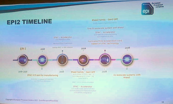
Given the timing for SiPearl's Rhea 2 and the company's natural with to preserve software compatibility with Rhea 1, it is reasonable to expect the processor to adopt Arm's Neoverse V3 cores for its second processor. Arm's Neoverse V3 offer quite a significant uplift compared to Neoverse V2 (and V1) and can scale to up to 128 cores per socket, which should be quite decent for HPC applications in 2025 – 2026.
While SiPearl will continue developing CPUs, it remains to be seen whether EPI will manage to deliver AI and HPC accelerators that are competitive against those from NVIDIA, AMD, and Intel.
More...
-
03-11-24, 07:42 AM #12056
Anandtech: The be quiet! Pure Power 12 M 650W PSU Review: Solid Gold
Be quiet! is renowned for its dedication to excellence in the realm of PC components, specializing in products that emphasize silence and performance. The brand's product lineup is extensive, encompassing high-quality power supply units (PSUs), cases, and cooling solutions, including air and liquid coolers. Be quiet! is particularly renowned for trying to achieve whisper-quiet operation across all its products, making it a favorite among PC enthusiasts who prioritize a noiseless computing environment. The brand's portfolio reflects a dedication to meeting the diverse needs of tech aficionados and professionals, with an array of products that emphasize noise reduction and efficiency.
This review shines a spotlight on the Be quiet! Pure Power 12 M 650W PSU, a standout product in Be quiet!'s PSU collection that illustrates the company's attitude towards product design. The Pure Power 12 M series is designed to provide dependable performance and quiet operation, catering to users who demand a good balance of power efficiency and acoustics with reliability and value. This model, in particular, strives to offer a compelling blend of performance and quality, making it an attractive option for individuals seeking a PSU that aligns with the requirements of both entry-level and advanced PC builds.
More...
-
05-30-24, 02:55 PM #12057
Anandtech: TSMC: Performance and Yields of 2nm on Track, Mass Production To Start In
In addition to revealing its roadmap and plans concerning its current leading-edge process technologies, TSMC also shared progress of its N2 node as part of its Symposiums 2024. The company's first 2nm-class fabrication node, and predominantly featuring gate-all-around transistors, according to TSMC N2 has almost achieved its target performance and yield goals, which places it on track to enter high-volume manufacturing in the second half of 2025.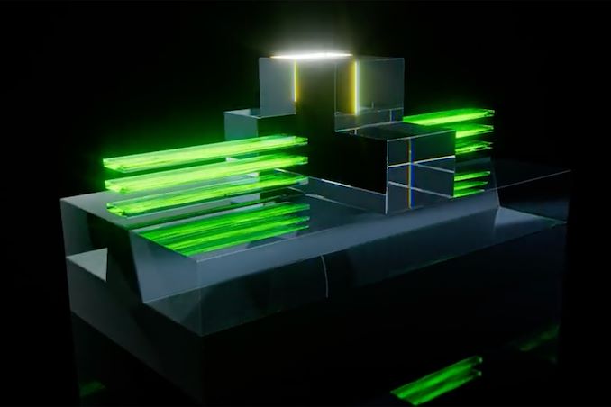
TSMC states that 'N2 development is well on track and N2P is next.' In particular, gate-all-around nanosheet devices currently achieve over 90% of their expected performance, whereas yields of 256 Mb SRAM (32 MB) devices already exceeds 80%, depending on the batch. All of this for a node that is over a year away from mass production.
Meanwhile, average yield of a 256 Mb SRAM was around 70% as of March, 2024, up from around 35% in April, 2023. Device performance has also been improving with higher frequencies being achieved while keeping power consumption in check.
Chip designer interest towards TSMC's first 2nm-class gate-all-around nanosheet transistor-based technology is significant, too. The number of new tape-outs (NTOs) in the first year of N2 is over two-times higher than it was for N5. Though with that said, given TSMC's close working relationship with a handful of high-volume vendors – most notably Appe – NTOs can be a very misleading figure since the first year of a new node at TSMC is capacity constrained, and consequently the bulk of that capacity goes to TSMC's priority partners.
Meanwhile, there were considerably more N5 tapeouts in its second year (some where N5P, of course) and N2 promises to have 2.6X more NTOs in its second year. So the node indeed looks quite promising. In fact, based on TSMC's slides (which we're unfortunately not able to republish), N2 is more popular than N3 in terms of NTOs both in the first and the second years of existence.
When it comes to the second year of N2, in the second half of 2026 TSMC plans to roll out its N2P technology, which promises additional performance and power benefits. N2P is expected to improve frequency by 15% - 20%, reduce power consumption by 30% - 40%, and increase chip density by over 1.15 times compared to N3E, significant benefits to move to all-new GAA nanosheet transistors.
Finally, for those companies that need the best in performance, power, and density, TSMC is poised to offer their A16 process in 2026. That node will also bring in backside power delivery, which will add costs, but is expected to greatly improve performance efficiency and scaling.
More...
-
05-30-24, 02:55 PM #12058
Anandtech: Lexar ARMOR 700 Portable SSD Review: Power-Efficient 2 GBps in an IP66 Pac
Lexar has a long history of serving the flash-based consumer storage market in the form of SSDs, memory cards, and USB flash drives. After having started out as a Micron brand, the company was acquired by Longsys which has diversified its product lineup with regular introduction of new products. Recently, the company announced a number of portable SSDs targeting different market segments. The Lexar ARMOR 700 Portable SSD makes its entry as the new flagship in the 20 Gbps PSSD segment.
Despite its flagship positioning and rugged nature, the ARMOR 700 is reasonably priced thanks to the use of a native USB flash controller - the Silicon Motion SM2320. Similar to the SL500, the product uses YMTC 3D TLC NAND (compared to the usual Micron or BiCS NAND that we have seen in SM2320-based PSSDs from other vendors). Read on for a detailed look at the ARMOR 700, including an analysis of its internals and evaluation of its performance consistency, power consumption, and thermal profile.
More...
-
05-31-24, 07:14 PM #12059
Anandtech: TSMC's 3D Stacked SoIC Packaging Making Quick Progress, Eyeing Ultra-Dense
TSMC's 3D-stacked system-on-integrated chips (SoIC) advanced packaging technologies is set to evolve rapidly. In a presentation at the company's recent technology symposium, TSMC outlined a roadmap that will take the technology from a current bump pitch of 9μm all the way down to a 3μm pitch by 2027, stacking together combinations of A16 and N2 dies.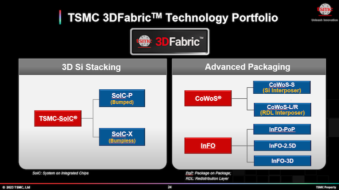
TSMC has a number of advanced packaging technologies, including 2.5D CoWoS and 2.5D/3D InFO. Perhaps the most intriguing (and complex) method is their 3D-stacked system-on-integrated chips (SoIC) technology, which is TSMC's implementation of hybrid wafer bonding. Hybrid bonding allows two advanced logic devices to be stacked directly on top of each other, allowing for ultra-dense (and ultra-short) connections between the two chips, and is primarily aimed at high performance parts. For now, SoIC-X (bumpless) is used for select applications, such as AMD's 3D V-cache technology for CPUs, as well as their Instinct MI300-series AI products. And while adoption is growing, the current generation of the technology is constrained by limitations on die sizes and interconnection pitches.
But those limitations are expected to give way quickly, if all goes according to plan for TSMC. SoIC-X technology is going to advance fast, and by 2027, it will be possible assemble a chip pairing a reticle-sized top die made on TSMC's leading-edge A16 (1.6nm-class) on a bottom die produced using TSMC's N2 (2nm-class). These dies, in turn, would be connected using 3μm bond pitche ssilicon vias (TSVs), three times the density of the size of today's 9μm pitch. Such small interconnections will allow for a much larger number of connections overall, greatly increasing the bandwidth density (and thus performance) of the assembled chip.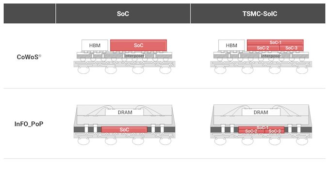
*TSMC considers reticle size as roughly 830 mm2.TSMC's SoIC-X Roadmap
Data by TSMC (Compiled by AnandTech)2022 2023 2024 2025 2026 2027 Top Die N7 N5 N4 N4 N2 A16 Bottom Die N7 ≥N6 ≥N5 ≥N4 ≥N3 ≥N2 Bond Pitch 9 μm 9 μm 6 μm 6 μm 4.5 μm 3 μm Size* 0.1 reticle 0.4 reticle 0.8 reticle 1 reticle 1 reticle 1 reticle
Improved hybrid bonding techniques are intended to allow TSMC's big HPC customers – AMD, Broadcom, Intel, NVIDIA, and the like – to build large, ultra-dense disaggregated processor designs for demanding applications, where distance between the dies is critical, as is the overall floor space used. Meanwhile, for applications where only performance matters, it will be possible to place multiple SoIC-X packages on a CoWoS interposer to get improved performance at a lower power consumption.
In addition to developing its bumpless SoIC-X packaging technology aimed at devices that require extreme performance, TSMC will also launch its bumped SoIC-P packaging process in the near future. SoIC-P is designed for cheaper lower performance applications that still want 3D-stacking, but don't need the additional performance and complexity that comes with bumpless copper-to-copper TSV connections. This packing technique will enable a broader range of companies to leverage SoIC, and while TSMC can't speak for their customers' plans, a cheaper version of the technology may make it accessible for more cost-conscious consumer applications.
Per TSMC's current plans, by 2025 the company will offer a face-to-back (F2B) bumped SoIC-P technology capable of pairing a 0.2-reticle sized N3 (3nm-class) top die with an N4 (4nm-class) bottom die, which will be connected using 25μm pitch microbumps (µbumps). In 2027, TSMC will introduce bumped face-to-face (F2F) SoIC-P technology, which will be able to place an N2 top die on an N3 bottom die with a pitch of 16μm.
*TSMC considers reticle size as roughly 830 mm2TSMC's SoIC-P Roadmap
Data by TSMC (Compiled by AnandTech)2025 2027 Top Die N3 N2 Bottom Die ≥N4 ≥N3 Bond Pitch 25 μm 16 μm Size* 0.2 reticle 0.4 reticle Die Orientation face-to-back face-to-face Qualification Time Q4 2024 for mobile SoC Q2 2026 for HPC
A lot of work has to be done to make SoIC more popular and accessible among chip developers, including continuing to iprove their die-to-die interfaces. But TSMC seems to be very optimistic about SoIC adoption by the industry, and expects around 30 SoIC designs to be released by 2026 – 2027.
More...
-
05-31-24, 07:14 PM #12060
Anandtech: GEEKOM A7 mini-PC Review : Premium Phoenix in a Compact 4x4 Package
The introduction of the Intel NUC in the early 2010s kickstarted the ultra-compact form-factor (UCFF) trend for desktop systems. Processors with TDPs ranging from 6 - 15W formed the backbone of this segment in the initial years. The emergence of configurable TDPs for notebook processors has prompted some vendors to introduce UCFF systems with regular 45W TDP processors (albeit, in cTDP-down mode).
GEEKOM, the private label brand of Shenzhen Jiteng Network Technology Co., has emerged as a popular UCFF system vendor in the last couple of years. After starting off with systems based on older processors, the company has moved on to introducing units carrying the latest and greatest from both AMD and Intel. The company has also been innovating on the form-factor side with compact boards smaller than the traditional 4"x4" ones in the NUC clones. The GEEKOM A7 is one such system based on AMD's Phoenix lineup.
The system is available in two configurations - one with the Ryzen 7 7840HS, and the other with the Ryzen 9 7940HS. The company sent over the flagship configuration to put through our evaluation routine for small form-factor computing systems. Read on to explore the performance profile and value proposition of the system, along with a discussion of the trade-offs involved in cramming a powerful notebook processor inside a system smaller than the traditional NUC.
More...


 Quote
QuoteThread Information
Users Browsing this Thread
There are currently 8 users browsing this thread. (0 members and 8 guests)


Bookmarks