

Results 2,661 to 2,670 of 12094
Thread: Anandtech News
-
02-19-13, 08:30 AM #2661
Anandtech: NVIDIA Announces Tegra 4i, Formerly Project Grey, With Integrated LTE and
It has been a while since we’ve heard anything about Project Grey, the first NVIDIA SoC with an integrated digital baseband, and the result of NVIDIA’s acquisition of soft-modem manufacturer Icera. Today, NVIDIA is ready to formalize Project Grey as Tegra 4i, and we have a bunch of information about this SoC and will obtain even more before MWC is upon us. NVIDIA’s roadmap from late 2011 put Grey in early 2013, and while other members of that roadmap haven’t necessarily stuck to the promised release schedule, Grey seems to be somewhere close to that schedule, at least as far as announcement and samples are concerned.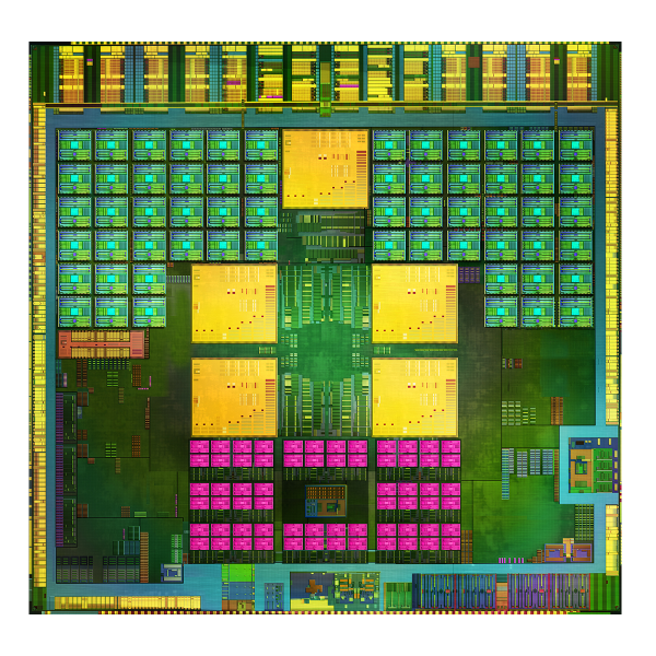
First, Tegra 4i includes the familiar 4+1 arrangement of cores we've seen since Tegra 3, but instead of Tegra 4's A15s, 4i includes ARM Cortex A9 CPUs running at a maximum single core clock of 2.3 GHz, we’re still waiting on a breakdown of the clock rates for dual and quad configuration, as well as the shadow core. NVIDIA has noted that it using R4 of ARM’s Cortex A9, which includes higher IPC thanks to the addition of a better data prefetching engine, dedicated hardware for cache preload instructions and some larger buffers. NVIDIA believes it is the first to implement the latest version of ARM's Cortex A9 core, however there's nothing stopping others from doing the same. 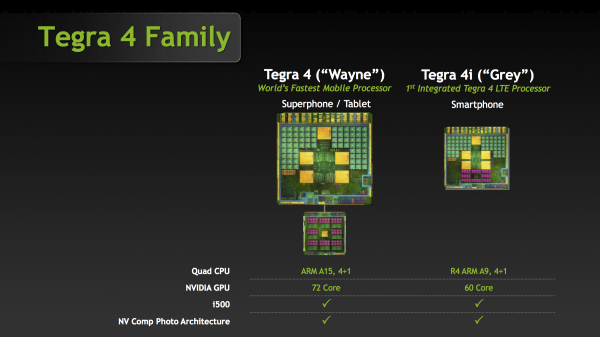
NVIDIA likely chose to integrate ARM's Cortex A9 r4 instead of the Cortex A15 to reduce power consumption and die size. While Tegra 4 is expected to be around 80mm^2, Tegra 4i measures in at around 60mm^2 including integrated baseband. NVIDIA isn't talking about memory interfaces at this point, but do keep in mind that your memory interface is often defined by the size of your die.
The 4i SoC is also built on TSMC’s 28 HPM process, interestingly enough not the 28 HPL process used for Tegra 4. As Tegra 4i appears to be geared towards hitting very high clock speeds, the use of TSMC's 28nm HPM process makes sense.
Tegra 4i also gets the exact same ISP and computational photography features that Tegra 4 includes, along with the same video encode and decode blocks. When it comes to the GPU side, 4i includes 60 GPU cores, that's just shy of the 72 in Tegra 4 proper. We’re waiting on additional detail to understand if these cores include the same enhancements we saw in Tegra 4 vs. Tegra 3. We also don't know the clock speed of the GPU cores in Tegra 4i.
Tegra 4i also includes the Icera i500 baseband IP block on-die, hence i for Icera. NVIDIA has disclosed some additional detail about i500 along the lines of what we’ve already written about. There’s full support for Category 3 (100 Mbps) LTE at launch, with a later upgrade to Category 4, along with support for 10 MHz + 10 MHz LTE carrier aggregation. In addition there’s support for the rest of the 3GPP suite of air interfaces, including WCDMA / HSPA+ up to 42 Mbps (Category 24), TD-SCDMA, and GSM/EDGE. i500 is also voice enabled with VoLTE support and CS-FB voice modes. NVIDIA claims that the i500 package is 7x7mm with a 6.5x6.5mm transceiver, and there are a total of 8 primary Rx ports (bands). NVIDIA also claims support for both 2x2 MIMO and 4x4 MIMO transmission modes on LTE. Tegra 4 Comparison   Tegra 4 Tegra 4i CPU Configuration 4+1 ARM Cortex A15 4+1 ARM Cortex A9 "r4" Single CPU Max Clock 1.9 GHz 2.3 GHz Process 28nm HPL 28nm HPM GPU Cores 72 60 Memory Interface PCDDR3 and LPDDR3 LPDDR3 Display 3200x2000 1920x1200 Baseband No Integrated Modem Icera i500
LTE Cat 3/Cat 4+CA TDD,FDD
100-150 Mbps DL (50 Mbps UL)  
TMs 1-8
WCDMA Cat 24/6 42 Mbps
DL (5.7 Mbps UL)Cat 24/6
TD-HSPA 4.2 Mbps DL
(2.2 Mbps UL) Including TD-SCDMAPackage 23x23 BGA
14x14 FCCSP12x12 POP
12x12 FCCSP
Functionally Tegra 4i is more like a heavily upgraded Tegra 3 than a Tegra 4 part thanks to the Cortex A9s.  It's clear that Tegra 4i is aimed more at the smartphone market while Tegra 4 proper aims at tablets or other platforms with a higher power budget and greater performance demands. 
In terms of time frame, NVIDIA expects the first Tegra 4i designs to begin shipping at the end of 2013, with most devices appearing in Q1 of 2014. It'll be interesting to see how a Cortex A9 based design holds up in Q1 2014, although the newer core and very high clock speed should do a good job of keeping the SoC feeling more modern than you'd otherwise expect.
The other big announcement is a reference design built around Tegra 4i called Phoenix. It's a smartphone with Tegra 4i inside, 5-inch 1080p display, LTE, and just 8 mm of thickness. What's more impressive is that NVIDIA claims the reference design can be picked up by an OEM and ship with an unsubsidized price tag of between $100-$300 USD. With Phoenix NVIDIA now joins the likes of Qualcomm and Intel, both of whom already have active smartphone reference design programs.
We have a lot more questions about Tegra 4, 4i, and Phoenix, but answers are coming.


More...
-
02-19-13, 10:00 AM #2662
Anandtech: Hands on and Impressions from the HTC One - Formerly M7
HTC is in an interesting position as a result of this last product cycle. While the previous HTC One series’ industrial design and performance was top notch, other OEMs still managed to eclipse the One series in terms of market adoption and consumer perception. Getting back to being a solid performer and cementing a place as at least the dominant number three player in the smartphone space is HTC’s mission for 2013, and the flagship device it’s starting that out with is the device previously known as M7, now known simply as the HTC One.
The choice of the HTC One name really emphasizes how much this launch means to HTC — this is the canonical One. This is the fullest expression of HTC’s view for what the One lineup should mean, this is their flagship. The One is a clear evolution of the industrial design first begun with the Butterfly and DNA, except instead of plastic the One is machined from a single solid block of aluminum. There are over 200 minutes of CNC machine cuts per device, which is a unibody construction. Plastic is injected into the aluminum block after certain cuts are made for the back case, which then gets machined into the final form. The One uses the top and bottom aluminum strips for antennas, both of which are actively tuned to mitigate unintended attenuation from being held. There’s a plastic insulative strip in-between the two antennas and the main body. In spite of being aluminum, the One also includes NFC, whose active area surrounds the camera region. There’s no wireless charging from Qi or WPC, however.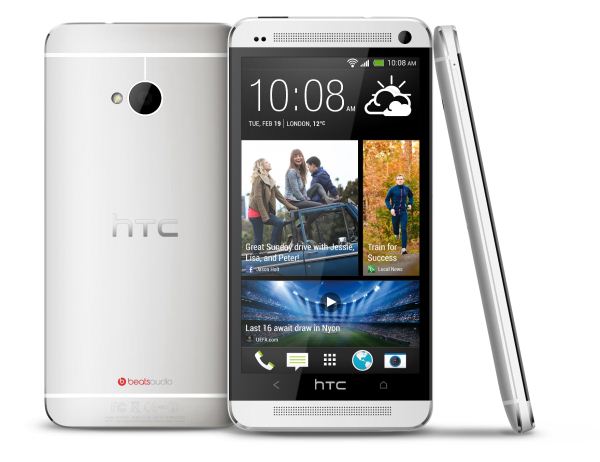
In the hands the HTC One has the kind of fit and finish that I’d expect from a high end device. I thought that the One S was perhaps the best industrial design of 2012 in part thanks to the metal backside, unique concave shape, and size. The truth is that the HTC One feels even better than that. There’s something inescapable about metal — HTC described it as expensive and luxurious feeling, like a well crafted tool. Other OEMs with metal phones like to evoke imagery of watches or high end jewelry. I think at some fundamental level metal does imply value, and as a result it conveys a much higher end in-hand feel than other entirely polycarbonate plastic designs. There’s a thin strip of plastic which runs around the edge of the device, and it’s here that the microSIM tray, ejection port, primary microphone, microUSB port, power/lock button (which doubles as IR transmit and receive), earphone jack, and volume rocker sit. The front has two aluminum pieces which serve as the speaker, microphone, and earpiece grilles. The HTC One will come in both an uncolored silver version, and anodized black.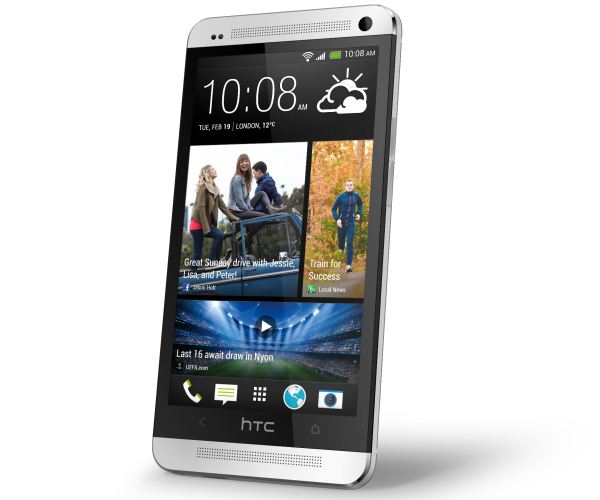
The One is topped with a 4.7-inch 1080p Super LCD 3 display. We’ve said that 2013 is going to be the year of 5-inch phones, and 4.7 is just shy. I think there’s something almost optimal about the device size that results with a 16:9 display size just short of 5-inches diagonal. It’s still possible to one hand if you have medium sized hands, easy to pocket, and still not laughably huge.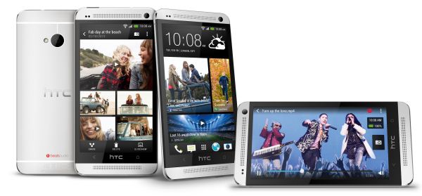
The HTC One at first glance might seem reminescent of another big metal unibody device, but in the hand couldn’t feel any more different. The convex rounded back side gives the One an entirely different in-hand feel, and the edges have a slight negative angle to them in addition to two chamfers.
Rather than place the primary speaker on the backside of the One, HTC has placed a set of speakers on the front of the device, one at top, one at bottom, behind the two grilles. These two provide stereo sound, and placing them on the front instead of the bottom or back makes a lot of sense for things like watching video, Google Navigation, and listening to music. The One also has dual microphones for noise rejection on calls, and also two different microphone pairs for accommodating low volume and high volume environments when recording audio. For example the commodity microphones generally included in a smartphone saturate around 70 dBA, HTC claims the dual microphone system on the One can accommodate up to 120 dBA SPL (Sound Pressure Level) without saturating.
At the core of the HTC One is a Snapdragon 600 (APQ8064Pro) SoC at 1.7 GHz. This is quad core Krait 300 (as opposed to 200 in MSM8960 or APQ8064) which brings a 15 percent increase in IPC as well as higher clocks (from 1.5 to 1.7 GHz), for about 20–30 percent higher overall CPU performance. This is still built on a 28nm LP process, and is analogous to the MSM8960Pro change from Krait 200 to 300, but for APQ8064. HTC One includes 2 GB of LPDDR2 RAM on a PoP in a 2x32 configuration. For storage, there’s no microSD card slot, but instead 32 or 64 GB of internal memory with no option for lesser 16 GB configurations. For connectivity the HTC One uses the same MDM9x15 baseband we’ve seen in Fusion 3 phones and in other places, and as expected the HTC One will come in LTE-enabled flavors for the appropriate operators. There’s still no magical single SKU that will do every region, but the most important band combinations are supported. On the WiFi side the HTC One is the first device I’m aware of to include 802.11ac support as well, alongside the usual a/b/g/n, this is provided by Broadcom’s latest combo, BCM4335.
The One continues to use the pyramidal internal stacking of display, then battery, then PCB which started with earlier designs. As a result the One includes an internal 2300 mAh 3.8V (8.74 Whr) battery which should be more than adequate in conjunction with Snapdragon 600 to provide good battery life.
[TR="class: tgrey"]
[TD="colspan: 5, align: center"] HTC One Specifications[/TD]
[/TR]
[TR="class: tlblue"]
[TD="class: tlgrey, width: 120"] Device[/TD]
[TD="width: 85, align: center"] HTC One[/TD]
[/TR]
[TR]
[TD="class: tlgrey"] SoC[/TD]
[TD="align: center"] 1.7 GHz Snapdragon 600
(APQ8064Pro - 4 x Krait 300 CPU, Adreno 320 GPU)[/TD]
[/TR]
[TR]
[TD="class: tlgrey"] RAM/NAND/Expansion[/TD]
[TD="align: center"] 2GB LPDDR2, 32/64 GB NAND[/TD]
[/TR]
[TR]
[TD="class: tlgrey"] Display[/TD]
[TD="align: center"] 4.7-inch SLCD3 1080p, 468 ppi[/TD]
[/TR]
[TR]
[TD="class: tlgrey"] Network[/TD]
[TD="align: center"] 2G / 3G / 4G LTE (Qualcomm MDM9x15 UE Category 3 LTE)[/TD]
[/TR]
[TR]
[TD="class: tlgrey"] Dimensions[/TD]
[TD="align: center"] 137.4 x 68.2 x 9.3mm max / 4mm min, 143 grams[/TD]
[/TR]
[TD="class: tlgrey"] Camera[/TD]
4.0 MP (2688
More...
-
-
02-19-13, 11:30 PM #2664
Anandtech: The new Opteron 6300: Finally Tested!
AMD unveiled their Opteron 6300 series server processors, code name Abu Dhabi, back in November 2012. At that time, no review samples were available. The numbers that AMD presented were somewhat confusing, as the best numbers were produced running the hard to assess SPECJbb2005 benchmark; the SPEC CPU2006 benchmarks were rather underwhelming.
Both benchmarks have only a distant link to real server workloads, and we could conclude only two things. Firstly, performance per GHz has improved and power consumption has gone down. Secondly, we are only sure that this is the case with well optimized, even completely recompiled code. The compiler settings of SPEC CPU 2006 and the JVM settings of Specjbb are all code that does not exist on servers running real applications.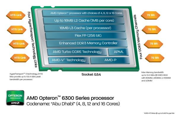
So is the new Opteron "Abu Dhabi" a few percent faster or is it tangibly faster when running real world code? And are the power consumption gains marginal at best or measurable? Well, most of our benchmarks are real world, so we will find out over the next several pages as we offer our full review of the Opteron 6300.

More...
-
02-20-13, 05:33 AM #2665
Anandtech: OCZ Releases Vertex 3.20 with 20nm IMFT NAND
Yesterday OCZ introduced an updated version of their Vertex 3: The Vertex 3.20. The name derives from the fact that the new Vertex 3.20 uses 20nm IMFT MLC NAND, whereas the original Vertex 3 used 25nm IMFT NAND. OCZ did the same with Vertex 2 and it's a common practice to move to smaller lithography NAND when it becomes cost-effective. At first the new lithography NAND may be more expensive and limited in availability but once the process matures, prices start to fall and eventually will overtake the old process node. Fortunately OCZ has learned from their mistakes and now the Vertex 3 with new NAND is easily distinguishable from the original Vertex 3, unlike with the Vertex 2 when OCZ silently switched to 25nm NAND.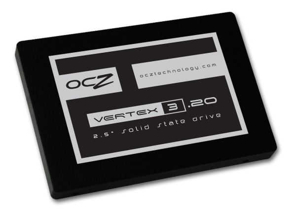
I asked OCZ why only Vertex 3 was updated with 20nm NAND and OCZ told me that the 20nm NAND is slower than 25nm. Intel initially told me that their 20nm NAND is as fast as their 25nm NAND (only erase time is slightly slower but that shouldn't impact end-user performance), though it should be kept in mind that OCZ uses NAND from Micron too and their binning process may be different from Intel's. Either way, it doesn't make sense (at least yet) for OCZ to update their high-end SSDs with the slower 20nm NAND, which is why Vertex 4 and Vector will stick with 25nm IMFT NAND.   Vertex 3.20 Vertex 3 Capacity 120GB 240GB 120GB 240GB Controller SandForce SF-2281 NAND 20nm IMFT MLC NAND 25nm IMFT MLC NAND Sequential Read 550MB/s 550MB/s 550MB/s 550MB/s Sequential Write 520MB/s 520MB/s 500MB/s 520MB/s 4KB Random Read 40K IOPS 35K IOPS 20K IOPS 40K IOPS 4KB Random Write 40K IOPS 65K IOPS 60K IOPS 60K IOPS
In other news, OCZ is also looking to phase out Agility 3 and 4 models. If you've been reading about OCZ's new business strategy (in a nutshell, less products and more focus on high-end market), this move makes a lot of sense because Agility has always been a compromised budget lineup. In the near future the Vertex 3.20 will be OCZ's mainstream model, which is why it was important for OCZ to cut the costs by moving to smaller process node NAND. 

More...
-
02-20-13, 11:30 AM #2666
Anandtech: Fractal Design Define XL R2 Case Review: Maybe We Can Have It All?
Amusingly and appropriately enough, the wave of silence-oriented enclosures that have been popping up recently haven't really drawn attention to themselves as a trend. Yet all of a sudden, we have results from a couple of solid contenders from Nanoxia and a few less expensive (and more readily available) also-rans. For a little while, this was a wave that Fractal Design was riding high, but the Define R4 wound up being a little underwhelming. As it turns out, they might just have something better lying in wait.
We never had a chance to play with the original Fractal Design Define XL, so it's tough to draw a direct comparison there. Yet one look at Fractal Design's page for the original tells you that while the Define R4 didn't change much from the R3, the Define XL R2 is a major shift. The original XL didn't support E-ATX; it was more just a conventional Define with a separate drive compartment. This R2, on the other hand, really is a giant Define R4. As it turns out, that bump in size and modest increase in cooling capacity may very well have been all the Define R4 needed..jpg)

More...
-
02-20-13, 11:30 AM #2667
Anandtech: Intel Demos CloverTrail+ Based Lenovo IdeaPhone K900 Ahead of MWC
Lenovo announced its ultra slim (6.9mm) 5.5" 1080p IdeaPhone K900 at CES earlier this year, based on Intel's presently unannounced CloverTrail+ SoC. While we're expecting to learn a lot more about CT+ next week at MWC, Intel did post a video showcasing the K900's performance. The video below includes footage of the K900 running Epic's Citadel for Android very smoothly at 1080p, as well as PR TextureMark.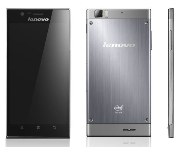
PR TextureMark is a video decode/GPU texturing/memory bandwidth benchmark, although Intel was careful not to actually run the benchmark on the phone. Intel's Atom SoCs have always been very good on the memory interface side compared to the ARM competition, which makes PR TextureMark an obvious showcase for the platform.
Epic's Citadel runs well on the K900, but as we showed earlier, it runs well on just about every high-end Android smartphone at this point. It's clear that the CT+ based K900 however integrates a much better GPU than the PowerVR SGX 540 included in Medfield, as the latter wouldn't be able to run Citadel at 1080p this smoothly.
I should also point out that some have been incorrectly assuming that the K900 is based on Intel's forthcoming Merrifield silicon. Merrifield and the rest of Intel's 22nm SoC lineup isn't due to ship/sample until the latter part of this year. Lenovo's K900 will be available in China starting in April, and expanding to other territories afterwards.

More...
-
02-20-13, 12:30 PM #2668
Anandtech: Samsung Details Exynos 5 Octa Architecture & Power at ISSCC '13
At CES this year Samsung introduced the oddly named Exynos 5 Octa SoC, one of the first Cortex A15 SoCs to implement ARM's big.LITTLE architecture. Widely expected to be used in the upcoming Galaxy S 4, the Exynos 5 Octa integrates 4 ARM Cortex A7 cores and 4 ARM Cortex A15 cores on a single 28nm LP HK+MG die made at Samsung's own foundry. As we later discovered, the Exynos 5 Octa abandons ARM's Mali GPU for Imagination's PowerVR SGX 544MP3, which should give it GPU performance somewhere between an iPad 3 and iPad 4.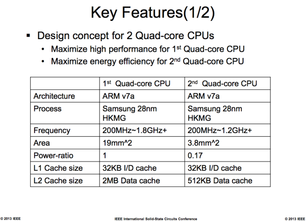
The quad-core A7 can run at between 200MHz and 1.2GHz, while the quad-core A15 can run at a range of 200MHz to 1.8GHz. Each core can be power gated independently. The idea is that most workloads will run on the quad-core A7, with your OS hot plugging additional cores as performance demands increase. After a certain point however, the platform will power down the A7s and start switching over to the A15s. Both SoCs implement the same revision of the ARM ISA, enabling seamless switching between cores. While it's possible for you to use both in parallel, initial software implementations will likely just allow you to run on the A7 or A15 clusters and switch based on performance requirements.
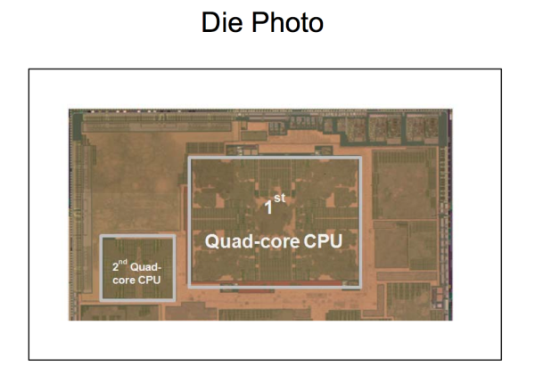
What's most interesting about Samsung's ISSCC presentation is we finally have some hard power and area data comparing the Cortex A15 to the Cortex A7. The table above puts it into numbers. The quad-core A15 cluster occupies 5x the area of the quad-core A7 cluster, and consumes nearly 6x the power in the worst case scenario. The area difference is artificially inflated by the fact that the A15 cluster has an L2 cache that's 4x the size of the A7 cluster, but looking at the die photo below you can get a good feel for just how much bigger the A15 cores are themselves:
In its ISSCC presentation, Samsung stressed the value of its custom libraries, timing tweaks and process technology selection in bringing the Exynos 5 Octa to market. Samsung is definitely marching towards being a real player in the SoC space and not just another ARM licensee.
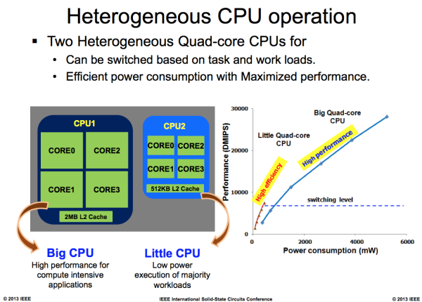
The chart below is one of the most interesting, it shows the relationship between small integer code performance and power consumption on the Cortex A7 and A15 clusters. Before switching from the little CPU to the big one, power consumption is actually quite reasonable - south of 1W and what you'd expect for a smartphone or low power tablet SoC. At the lower end of the performance curve for the big CPU things aren't too bad either, but once you start ramping up clock speed and core count power scales linearly. Based on this graph, it looks like it takes more than 3x the power to get 2x the performance of the A7 cluster using the Cortex A15s.
 
Gallery: Samsung Details Exynos 5 Octa Architecture & Power at ISSCC '13


More...
-
02-20-13, 03:30 PM #2669
Anandtech: An Update on Intel's SSD 525 Power Consumption
Intel's SSD 525 is the mSATA version of last year's SF-2281 based Intel SSD 520. The drive isn't just physically smaller, but it also features a new version of the Intel/SandForce firmware with a bunch of bug fixes as well as some performance and power improvements. Among the improvements is a tangible reduction in idle power consumption. However in our testing we noticed higher power consumption than the 520 under load. Intel hadn't seen this internally, so we went to work investigating why there was a discrepancy.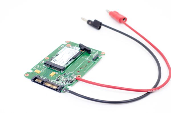
The SATA power connector can supply power to a drive on a combination of one or more power rails: 3.3V, 5V or 12V. Almost all 2.5" desktop SSDs draw power on the 5V rail exclusively, so our power testing involves using a current meter inline with the 5V rail. The mSATA to SATA adapter we use converts 5V to 3.3V for use by the mSATA drive, however some power is lost in the process. In order to truly characterize the 525's power we had to supply 3.3V directly to the drive and measure at our power source. The modified mSATA adapter above allowed us to do just that.
Idle power consumption didn't change much:
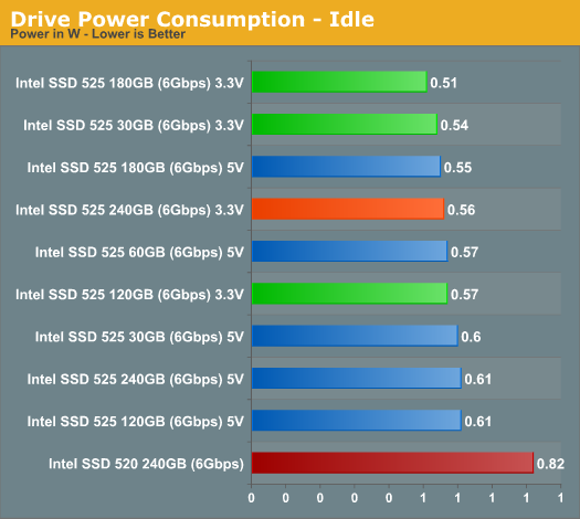 Note that the 525 still holds a tremendous advantage over the 2.5" 520 in idle power consumption. Given the Ultrabook/SFF PC/NUC target for the 525, driving idle power even lower makes sense.Under load there's a somewhat more appreciable difference in power when we measure directly off of a 3.3V supply to the 525:Our 520 still manages to be lower power than the 525, however it's entirely possible that we simply had a better yielding NAND + controller combination back then. There's about a 10 - 15% reduction in power compared to measuring the 525 at the mSATA adapter's 5V rail with the 240GB model.
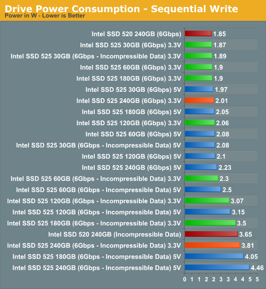
There story isn't any different in our random write test. Measuring power sent direct to the 525 narrows the gap between it and our old 520 sample. Our original 520 still seems to hold a small active power advantage over our 525 samples, but with only an early sample to compare to it's impossible to say if the same would be true for a newer/different drive. 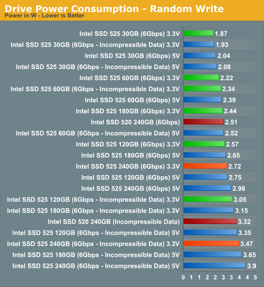
I've updated Bench to include the latest power results.

More...
-
02-20-13, 07:00 PM #2670
Anandtech: Sony Announces PlayStation 4: PC Hardware Inside
Sony just announced the PlayStation 4, along with some high level system specifications. The high level specs are what we've heard for quite some time: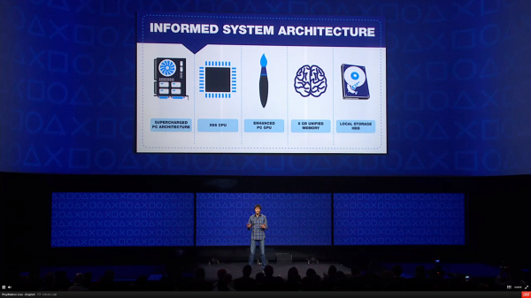
- 8-core x86 CPU (built by AMD)
- High-end PC GPU (also built by AMD), delivering almost 2 TFLOPS of performance.
- Unified 8GB of GDDR5 memory for use by both the CPU and GPU with 176GB/s of memory bandwidth
- Large local hard drive
Details of the CPU aren't known at this point (8-cores could imply a Piledriver derived architecture, or 8 smaller Jaguar cores - the latter being more likely), but either way this will be a big step forward over the PowerPC based general purpose cores on Cell from the previous generation. I wouldn't be too put off by the lack of Intel silicon here, it's still a lot faster than what we had before and at this level price matters more than peak performance. The Intel performance advantage would have to be much larger to dramatically impact console performance. If we're talking about Jaguar cores, then there's a bigger concern long term from a single threaded performance standpoint. Backwards compatibility with PS3 games isn't guaranteed and instead will leverage cloud gaming to stream older content to the box.
There's some sort of a dedicated background processor that handles uploads and downloads, and even handles updates in the background while the system is off. The PS4 also supports instant suspend/resume.
We don't know specifics of the GPU, but with approaching 2 TFLOPS we're looking at a level of performance somewhere between a Radeon HD 7850 and 7870. The highest end PC GPUs are already faster than this, but the PS4's GPU is a lot faster than the PS3's RSX which was derived from NVIDIA's G70 architecture (used in the GeForce 7800 GTX, for example). 
Outfitting the PS4 with 8GB of RAM will be great for developers, and using high-speed GDDR5 will help ensure the GPU isn't bandwidth starved. Sony promised around 176GB/s of memory bandwidth for the PS4.
Leveraging Gaiki's cloud gaming technology, the PS4 will be able to act as a game server and stream the video output to a PS Vita, wirelessly. This sounds a lot like what NVIDIA is doing with Project Shield and your NVIDIA powered gaming PC. Sony referenced dedicated video encode/decode hardware that allows you to instantaneously record and share screenshots/video of gameplay. I suspect this same hardware is used in streaming your game to a PS Vita.
The lack of solid state storage isn't surprising. Hard drives still offer a dramatic advantage in cost per GB vs. an SSD. Now if it's user replaceable with an SSD that would be a nice compromise.
The new box heavily leverages PC hardware, which is something we're expecting from the next Xbox as well. It's interesting that this is effectively how Microsoft entered the console space back in 2001 with the original Xbox, and now both Sony and MS have returned to that philosophy with their next gen consoles in 2013. 
I'm trying to get more details on the CPU and GPU architectures and will update as soon as I have more info.

More...


 Quote
Quote
Thread Information
Users Browsing this Thread
There are currently 16 users browsing this thread. (0 members and 16 guests)


Bookmarks