

Results 3,761 to 3,770 of 12096
Thread: Anandtech News
-
03-26-14, 12:30 PM #3761
Anandtech: AMD Announces FirePro W9100
In what’s proving to be a busy week for GPU news, AMD has just wrapped up their webcast announcing their next flagship FirePro product. Dubbed the FirePro W9100, AMD’s latest card is their expected refresh of their FirePro product lineup to integrate the company’s recently launched Hawaii family of processors.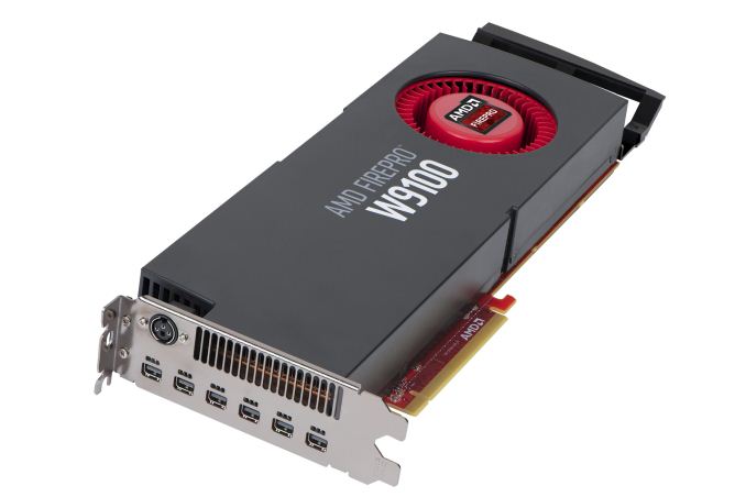
As Hawaii itself was a small but important refresh to Tahiti and the GCN architecture, the same can be said of the FirePro W9100 compared to the FirePro W9000. Other than some gaming-exclusive features such as TrueAudio, Hawaii’s biggest changes were the Asynchronous Compute Engine (ACE) additions that are part of GCN 1.1, the wider 4 primitive geometry pipeline, and of course the overall increase in performance and performance per watt compared to Tahiti. So from a technical perspective W9100 stands to be a relatively straightforward improvement to what W9000 has offered thus far.
[TABLE="align: center"]
[TR="class: tgrey"]
[TD="colspan: 7, align: center"] AMD FirePro W Series Specification Comparison[/TD]
[/TR]
[TR="class: tlblue"]
[TD="width: 171"] [/TD]
[TD="width: 113, align: center"] AMD FirePro W9100[/TD]
[TD="width: 113, align: center"] AMD FirePro W9000[/TD]
[TD="width: 118, align: center"] AMD FirePro W8000[/TD]
[TD="width: 119, align: center"] AMD FirePro W7000[/TD]
[/TR]
[TR]
[TD="class: tlgrey"] Stream Processors[/TD]
[TD="align: center"] 2816[/TD]
[TD="align: center"] 2048[/TD]
[TD="align: center"] 1792[/TD]
[TD="align: center"] 1280[/TD]
[/TR]
[TR]
[TD="class: tlgrey"] Texture Units[/TD]
[TD="align: center"] 176[/TD]
[TD="align: center"] 128[/TD]
[TD="align: center"] 112[/TD]
[TD="align: center"] 80[/TD]
[/TR]
[TR]
[TD="class: tlgrey"] ROPs[/TD]
[TD="align: center"] ?[/TD]
[TD="align: center"] 32[/TD]
[TD="align: center"] 32[/TD]
[TD="align: center"] 32[/TD]
[/TR]
[TR]
[TD="class: tlgrey"] Core Clock[/TD]
[TD="align: center"] ?[/TD]
[TD="align: center"] 975MHz[/TD]
[TD="align: center"] 900MHz[/TD]
[TD="align: center"] 950MHz[/TD]
[/TR]
[TR]
[TD="class: tlgrey"] Memory Clock[/TD]
[TD="align: center"] ?[/TD]
[TD="align: center"] 5.5GHz GDDR5[/TD]
[TD="align: center"] 5.5GHz GDDR5[/TD]
[TD="align: center"] 4.8GHz GDDR5[/TD]
[/TR]
[TR]
[TD="class: tlgrey"] Memory Bus Width[/TD]
[TD="align: center"] ?[/TD]
[TD="align: center"] 384-bit[/TD]
[TD="align: center"] 256-bit[/TD]
[TD="align: center"] 256-bit[/TD]
[/TR]
[TR]
[TD="class: tlgrey"] VRAM[/TD]
[TD="align: center"] 16GB[/TD]
[TD="align: center"] 6GB[/TD]
[TD="align: center"] 4GB[/TD]
[TD="align: center"] 4GB[/TD]
[/TR]
[TR]
[TD="class: tlgrey"] Double Precision[/TD]
[TD="align: center"] 1/2?[/TD]
[TD="align: center"] 1/4[/TD]
[TD="align: center"] 1/4[/TD]
[TD="align: center"] 1/16[/TD]
[/TR]
[TR]
[TD="class: tlgrey"] Transistor Count[/TD]
[TD="align: center"] 6.2B[/TD]
[TD="align: center"] 4.31B[/TD]
[TD="align: center"] 4.31B[/TD]
[TD="align: center"] 2.8B[/TD]
[/TR]
[TR]
[TD="class: tlgrey"] TDP[/TD]
[TD="align: center"] ?[/TD]
[TD="align: center"] 274W[/TD]
[TD="align: center"] 189W[/TD]
[TD="align: center"]
-
03-26-14, 06:30 PM #3762
Anandtech: The HTC One (M8) Review
HTC remains one of few Android OEMs insanely focused on design. Even dating back to the origins of the One brand in 2012 with the One X and One S, HTC clearly saw design where others were more focused on cost optimization. Only time will tell which is the more viable long term business strategy, but in the interim we’ve seen two generations of well crafted devices from what would otherwise be thought of as a highly unlikely source. With its roots in the ODM/OEM space, HTC is one of very few ODM turned retail success stories that we’ve seen come out of Taiwan. ASUS is the closest and only real comparison I can make.
As its name implies, the goal of the One brand was to have a device that anyone, anywhere in the world could ask for and know they were getting an excellent experience. Although HTC sort of flubbed the original intent by introducing multiple derivatives (One X, One S, One X+), it was the beginning of relief from the sort of Android OEM spaghetti we saw not too long ago. With the One brand, HTC brought focus to its product line.
Last year HTC took a significant step towards evolving the brand into one true flagship device, aptly named the One. Once again there were derivatives (One mini and One max), but the messaging was far less confusing this time around. If you wanted small you got the mini, if you wanted big you got the max, otherwise all you needed to ask for was the One.
With last year’s One (codenamed M7), HTC was incredibly ambitious. Embracing a nearly all metal design and opting for a much lower resolution, but larger format rear camera sensor, the One was not only bold but quite costly to make. With the premium smartphone market dominated by Apple and Samsung, and the rest of the world headed to lower cost devices, it was a risky proposition. From a product standpoint, I’d consider the M7 One a success. A year ago I found myself calling it the best Android phone I’d ever used.
It didn’t take long for my obsession to shift to the Moto X, and then the Nexus 5, although neither delivered the overall camera experience of the One. Neither device came close to equaling HTC on the design front either, although I maintain Motorola did a great job with in hand feel. Although I found myself moving to newer devices since my time with the One last year, anytime I picked up the old M7 I was quickly reminded that HTC built a device unlike any other in the Android space. It just needed a refresh.
This is our review of the new HTC One.
More...
-
03-27-14, 01:00 PM #3763
Anandtech: Corsair Graphite 760T Case Review
Corsair has been releasing one case after another lately, expanding their already large ranks with an even greater variety of products. It has been less than three months since the release of the Obsidian 250D, a cubic Mini-ITX case, and only two days since another member of the Obsidian series, the Midi-ATX Obsidian 450D, has been announced. Today, Corsair announced the release of yet another case, the Graphite 730T/760T. We've had the case for a few days, so read on for our review.
More...
-
03-27-14, 03:30 PM #3764
Anandtech: NVIDIA Announces Jetson TK1 Dev Board; Adds Erista To Tegra Roadmap
Continuing our coverage of NVIDIA’s 2014 GPU Technology Conference, today we’re looking at NVIDIA’s Tegra-related announcements. As Tegra is primarily a consumer facing product, especially the pre-K1 parts, NVIDIA centers the bulk of their Tegra announcements around the annual Consumer Electronics Show in January. So what is announced at GTC just 2 months later tends to focus on developers and professional uses of announced products.
With that said, while NVIDIA isn’t offering much in the way of architectural details at the moment, they have given us a GPU-centric roadmap update for the Tegra product line.
The new roadmap includes a new SoC called Erista, which we have limited details about. Scheduled for 2015, Erista will be based on a Maxwell GPU, affirming NVIDIA’s earlier commitments to get their Tegra line up to Maxwell in 2015. Unfortunately that’s all we know about it at this time; the CPU component, additional features, and manufacturing process have not been specified. That said, a little research shows that Erista is the son of Wolverine/Logan, so the fact that this isn’t a distinct product name but rather a name related to Logan (like Kayla last year) may offer a hint of what to expect.
NVIDIA's GTC 2013 Tegra Roadmap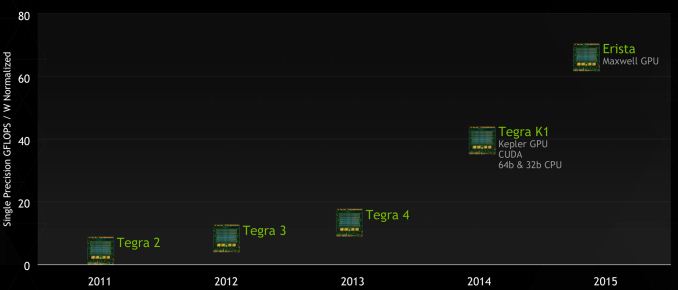
NVIDIA's GTC 2014 Tegra Roadmap
Not shown on this roadmap, but still in the pipeline, is NVIDIA’s alternative K1 design utilizing their Denver CPU rather than the ARM A15. The Denver K1 was announced back at CES, and from the perspective of this roadmap is equivalent to the A15 K1, since both utilize the same Kepler GPU. NVIDIA hasn’t offered up any additional Denver details at GTC, but we’re not expecting any this soon after CES, so we expect to hear more about it when the Denver K1 is closer to shipping (currently scheduled for H2 2014, likely the later part of that window).
However Parker is a mystery that we’re still tracking down. Parker is oddly not on this roadmap, and the introduction of Erista doesn’t help. Parker still is (as far as we know) a Denver + Maxwell + FinFET design, which overlaps with Erista’s unknown CPU + Maxwell design. Given that Denver K1 should be out this year and Maxwell is scheduled for next year regardless, the most questionable part of that combination is the FinFET aspect, presumably TSMC’s 16nm FinFET process. We’re still working on finding out more information on the current state of Parker, but we wouldn’t be surprised if Erista was the 20nm backup plan in case 16nm FinFET wasn’t ready in time.
Jetson “TK1”: A Tegra K1 Development Board
Roadmaps aside, this week’s Tegra announcements are short but significant for the GTC crowd. The highlight of the Tegra product announcements here is NVIDIA’s new Jetson “TK1” development board. Jetson follows in the footsteps of Kayla, which was NVIDIA’s prior Tegra development board and was announced at the previous GTC. But whereas Kayla was essentially a prototype – a 2 chip solution using a Tegra 3 and a GK208 PCIe card, mounted on a mini-ITX board and intended for early development testing of K1-like GPU performance – Jetson is the final product.
Jetson is composed of a Tegra K1 mounted on to smaller board (possibly Nano-ITX?), outfitted with 2GB of RAM and 16GB of NAND (eMMC) storage. The board provides a suite of I/O options including HDMI 1.4, analog audio in and out, GigE, SATA, mini-PCIe, USB, a suite of GPIOs, and an RS-232 serial port (apparently a highly demanded feature that Kayla lacked). NVIDIA’s release information doesn’t make mention of cooling, so at first glance this appears to be a bring-your-own-cooler affair, which shouldn’t be too difficult given K1’s sub-10W TDP.
Meanwhile Jetson’s software stack is composed of a 32bit version of Ubuntu 13.04 for Tegra processors. Layered on it is of course NVIDIA’s drivers and software stack, exposing OpenGL and the other common APIs on the graphics side, and CUDA and OpenCL on the compute side. Jetson will also be the first device to come with NVIDIA’s new VisionWorks middleware, which is a computer vision software package that provides APIs and software samples for a range of computational vision tasks, analogous to what the CUDA toolkit provided for GU programming and language development. VisionWorks includes code for augmented reality, computational photography, robotics, human machine interaction, and driver assistance systems. NVIDIA has big plans for K1 in embedded systems, and VisionWorks is one way they will be priming the pump, by providing some of the software themselves to bring on board new users early.
From a programming standpoint, K1 (and Jetson as a result) are Compute Capability 3.2, which is essentially the GK110 feature set minus the dynamic parallelism functionality, and including all of the integer, register, and thread improvements that differentiate GK110 from GK10x. On that note, it’s worth mentioning that while Jetson/K1 has a unified memory pool – the first such CUDA capable product due to the integration of Kepler – the actual memory architecture isn’t fully unified. NVIDIA is essentially at an AMD Llano level of integration; full integration will likely come in the future with newer GPUs and CPUs.
As we mentioned earlier, Jetson is first and foremost targeted towards hardware and software developers looking to further develop software for deployment on finalized K1-equipped devices (phones, tablets, cars, etc). However because Jetson is a complete, COTS K1 device, there is significant buzz around the show about just utilizing Jetson as it is. For smaller companies who don’t need the space savings and customization of building their own K1 device, Jetson can be used instead, especially in bigger devices where Jetson’s size is not a problem.
In fact the first K1 device we’ve seen up and running is a Jetson board, being utilized by GE Intelligent Platforms. GEIP is among the first Jetson users, and is showcasing the ability for Jetson/K1 to drive one of their combined camera/lidar sensors. The setup taps both the GPUs and CPUs to process data and identify the movement of objects, and interestingly despite the heavy workload from this kind of processing, only reaches approximately 75% resource utilization on Jetson. GEIP’s big market for this technology is of course defense applications (automated target identification) where they already do something similar with larger dGPU setups, but GEIP’s also investigating other uses such a medical, with a concept of a handheld ultrasound device.
Moving on, Jetson is expected to become available in April. NVIDIA is already taking pre-orders for Jetson over at their developer site, and in NVIDIA’s usually cheeky fashion will go for $192 – one dollar for every CUDA core on the K1. This also gives us an idea of when K1 consumer devices should be available, as the shorter lead time for Jetson (as opposed to radio certified mobile devices) means that NVIDIA can be shipping K1s for Jetson while also shipping K1s to their OEM customers for their devices.
On a lighter note, after some further investigation into the Jetson codename we’ve determined that NVIDIA has dropped their superhero codenames for this development board, finding no relation between “Jetson” and “Logan” or any other superhero. Our best guess is that NVIDIA is taking a futuristic spin, at least for development boards.
Finally, though it wasn’t covered in NVIDIA’s initial keynote, NVIDIA will be producing a second, better equipped board for automotive customers under the Jetson name. Dubbed Jetson Pro, the board is a customizable building block that uses a Tegra 3 processor as the core system component, with the I/O necessary to add on a number of different devices as an Enhanced Breakout Board (EBB). NVIDIA specifically notes that dGPUs are an option here, explaining the use of the relatively old Tegra 3, as it’s the most recent Tegra SoC to feature PCI-Express capabilities.

More...
-
03-28-14, 08:30 AM #3765
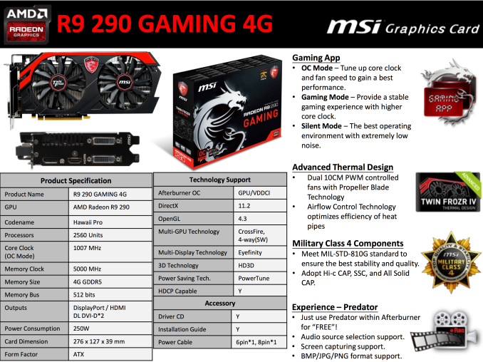
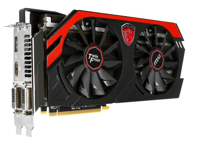
Anandtech: MSI Radeon R9 290 Gaming 4G Giveaway
Anyone looking to upgrade their gaming rig will be extremely excited about our next giveaway. MSI's Radeon R9 Gaming 4G features AMD's 6.2 billion transistor Hawaii GPU. The R9 290 launched last year at an MSRP of $399, but incredible demand from the coin mining community have kept its prices substantially higher since then.
If you've had troubles finding an R9 290 at MSRP post launch, MSI is about to solve that problem for two lucky AnandTech readers. We'll be drawing two winners at random, who will each receive an MSI Radeon R9 Gaming 4G graphics card. We'll be accepting entries until 3/31 at 12PM ET. To enter just leave a comment below (please only post once) and make sure you're a US resident with a US mailing address. For all entry details check out our official terms below. Good luck!
More...
-
03-31-14, 01:31 AM #3766
Anandtech: Apple's Cyclone Microarchitecture Detailed
The most challenging part of last year's iPhone 5s review was piecing together details about Apple's A7 without any internal Apple assistance. I had less than a week to turn the review around and limited access to tools (much less time to develop them on my own) to figure out what Apple had done to double CPU performance without scaling frequency. The end result was an (incorrect) assumption that Apple had simply evolved its first ARMv7 architecture (codename: Swift). Based on the limited information I had at the time I assumed Apple simply addressed some low hanging fruit (e.g. memory access latency) in building Cyclone, its first 64-bit ARMv8 core. By the time the iPad Air review rolled around, I had more knowledge of what was underneath the hood: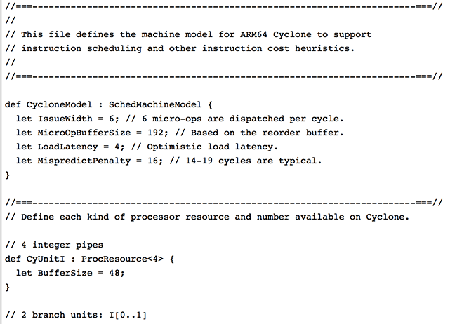
As far as I can tell, peak issue width of Cyclone is 6 instructions. That’s at least 2x the width of Swift and Krait, and at best more than 3x the width depending on instruction mix. Limitations on co-issuing FP and integer math have also been lifted as you can run up to four integer adds and two FP adds in parallel. You can also perform up to two loads or stores per clock.
With Swift, I had the luxury of Apple committing LLVM changes that not only gave me the code name but also confirmed the size of the machine (3-wide OoO core, 2 ALUs, 1 load/store unit). With Cyclone however, Apple held off on any public commits. Figuring out the codename and its architecture required a lot of digging.
Last week, the same reader who pointed me at the Swift details let me know that Apple revealed Cyclone microarchitectural details in LLVM commits made a few days ago (thanks again R!). Although I empirically verified many of Cyclone's features in advance of the iPad Air review last year, today we have some more concrete information on what Apple's first 64-bit ARMv8 architecture looks like.
Note that everything below is based on Apple's LLVM commits (and confirmed by my own testing where possible).
As I mentioned in the iPad Air review, Cyclone is a a wide machine. It can decode, issue, execute and retire up to 6 instructions/micro-ops per clock. I verified this during my iPad Air review by executing four integer adds and two FP adds in parallel. The same test on Swift actually yields fewer than 3 concurrent operations, likely because of an inability to issue to all integer and FP pipes in parallel. Similar limits exist with Krait.Apple Custom CPU Core Comparison Apple A6 Apple A7 CPU Codename Swift Cyclone ARM ISA ARMv7-A (32-bit) ARMv8-A (32/64-bit) Issue Width 3 micro-ops 6 micro-ops Reorder Buffer Size 45 micro-ops 192 micro-ops Branch Mispredict Penalty 14 cycles 16 cycles (14 - 19) Integer ALUs 2 4 Load/Store Units 1 2 Load Latency 3 cycles 4 cycles Branch Units 1 2 Indirect Branch Units 0 1 FP/NEON ALUs ? 3 L1 Cache 32KB I$ + 32KB D$ 64KB I$ + 64KB D$ L2 Cache 1MB 1MB L3 Cache - 4MB
I also noted an increase in overall machine size in my initial tinkering with Cyclone. Apple's LLVM commits indicate a massive 192 entry reorder buffer (coincidentally the same size as Haswell's ROB). Mispredict penalty goes up slightly compared to Swift, but Apple does present a range of values (14 - 19 cycles). This also happens to be the same range as Sandy Bridge and later Intel Core architectures (including Haswell). Given how much larger Cyclone is, a doubling of L1 cache sizes makes a lot of sense.
On the execution side Cyclone doubles the number of integer ALUs, load/store units and branch units. Cyclone also adds an indirect branch predictor and at least one more FP pipe. Cyclone can sustain three FP operations in parallel (including 3 FP/NEON adds). The third FP/NEON pipe is used for div and sqrt operations, the machine can only execute two FP/NEON muls in parallel.
I also found references to buffer sizes for each unit, which I'm assuming are the number of micro-ops that feed each unit. I don't believe Cyclone has a unified scheduler ahead of all of its execution units and instead has statically partitioned buffers in front of each port. I've put all of this information into the crude diagram below:
Unfortunately I don't have enough data on Swift to really produce a decent comparison image. With six decoders and nine ports to execution units, Cyclone is big. As I mentioned before, it's bigger than anything else that goes in a phone. Apple didn't build a Krait/Silvermont competitor, it built something much closer to Intel's big cores. At the launch of the iPhone 5s, Apple referred to the A7 as being "desktop class" - it turns out that wasn't an exaggeration.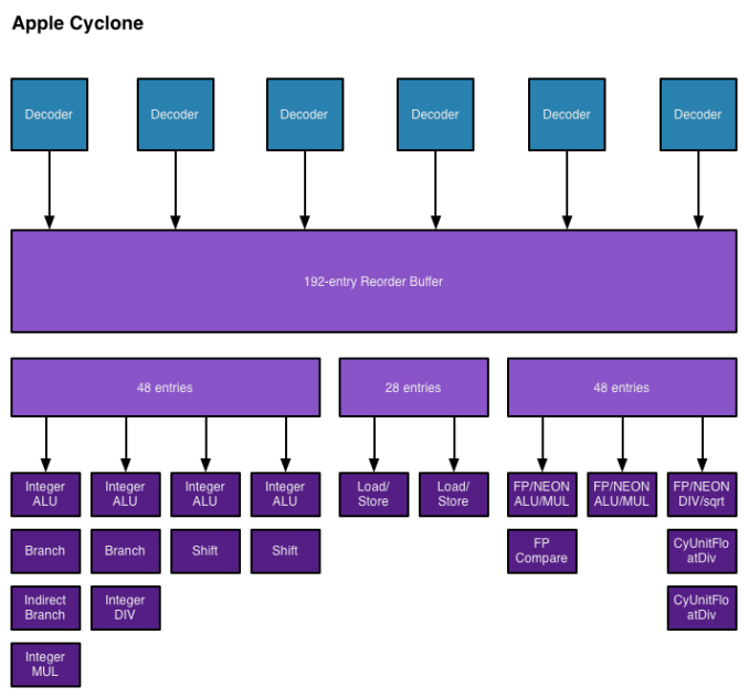
Cyclone is a bold move by Apple, but not one that isn't without its challenges. I still find that there are almost no applications on iOS that really take advantage of the CPU power underneath the hood. More than anything Apple needs first party software that really demonstrates what's possible. The challenge is that at full tilt a pair of Cyclone cores can consume quite a bit of power. So for now, Cyclone's performance is really used to exploit race to sleep and get the device into a low power state as quickly as possible. The other problem I see is that although Cyclone is incredibly forward looking, it launched in devices with only 1GB of RAM. It's very likely that you'll run into memory limits before you hit CPU performance limits if you plan on keeping your device for a long time.
It wasn't until I wrote this piece that Apple's codenames started to make sense. Swift was quick, but Cyclone really does stir everything up. The earlier than expected introduction of a consumer 64-bit ARMv8 SoC caught pretty much everyone off guard (e.g. Qualcomm's shift to vanilla ARM cores for more of its product stack).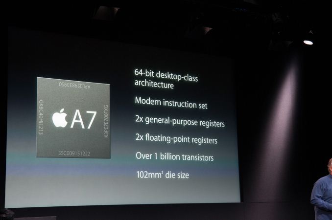
The real question is where does Apple go from here? By now we know to expect an "A8" branded Apple SoC in the iPhone 6 and iPad Air successors later this year. There's little benefit in going substantially wider than Cyclone, but there's still a ton of room to improve performance. One obvious example would be through frequency scaling. Cyclone is clocked very conservatively (1.3GHz in the 5s/iPad mini with Retina Display and 1.4GHz in the iPad Air), assuming Apple moves to a 20nm process later this year it should be possible to get some performance by increasing clock speed scaling without a power penalty. I suspect Apple has more tricks up its sleeve than that however. Swift and Cyclone were two tocks in a row by Intel's definition, a third in 3 years would be unusual but not impossible (Intel sort of committed to doing the same with Saltwell/Silvermont/Airmont in 2012 - 2014).
Looking at Cyclone makes one thing very clear: the rest of the players in the ultra mobile CPU space didn't aim high enough. I wonder what happens next round.
More...
-
03-31-14, 08:30 AM #3767
Anandtech: ARM Partners Ship 50 Billion Chips Since 1991 - Where Did They Go?
One of the great things about working with ARM is getting access to people and information comes without the usual hurdles. With most chipmakers or IP providers, getting publishable data is often an exercise in political maneuvering and calling in favors. If it's not officially sanctioned for disclosure we often have to prepare for an uphill battle. The traditional PC folks are a lot better than most of the mobile guys (who are thankfully beginning to come around). With ARM on the other hand, these days you just need to ask and have a good reason.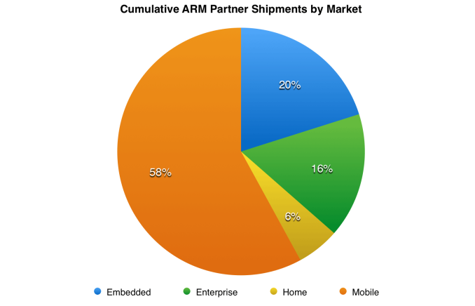
A few weeks ago ARM celebrated its partners shipping over 10 billion ARM based chips in 2013. As ARM makes a royalty on every IP license shipped, it was a banner year for the company. The bigger story was that the 10 billion in 2013 brought the cumulative total for ARM based processors to over 50 billion. ARM's press activities were limited to talking about the big final number, but ARM has a pretty broad IP portfolio. What I wanted was a breakdown of where the 50 billion went, so I asked.
What I got in response were tables of data. I was asked not to share specific numbers, but using the data in graphs was ok - and that's all I wanted to do. We'll start with where the 50 billion went in terms of markets (pictured above). Mobile obviously took the majority of shipments, followed by embedded markets. Remember that ARM cores are used all over the place, including in things like HDD and SSD controllers. The modems that work alongside the main apps processors in mobile devices are also frequently home to ARM processor IP. Intel's Quark project actually came about because Intel needed a low power/low cost core to use internally for various projects and eventually decided to offer it to anyone who wanted it. For those companies that don't have the desire/ability to build and validate their own low power CPU core, they often turn to ARM.
The enterprise slice may be a bit misleading depending on what you define as enterprise. We often refer to enterprise in terms of primary CPU shipments into servers. In this case we're talking about chips that go into things like routers and wireless access points. ARM obviously hopes to take a big portion of the high dollar enterprise CPU market with its ARMv8 based IP in the coming years, but it's not there yet.
The smallest slice, labeled home, is still nearly 3 billion shipments. Here we're talking about things like consumer set top boxes as well as wearables.
Note that 37.5 of the 50 billion chips shipped in the past five years (2009 - 2013). That shouldn't come as a surprise given the overlap between that time period and the rise of modern smartphones and tablets.
While ARM wasn't willing to give me shipments by specific core, it was willing to give me family data:
Two thirds of all ARM mobile shipments are really old ARM7 and ARM9 based designs (remember my point about modems above). Here we get the first hint that the reign of the ARM11 designs (the foundation of the original iPhone) was a small blip in the grand scheme of things - the Cortex A family is really what allowed mobile to grow.
The embedded market is dominated by these lower power cores, although the newer Cortex M designs have made a huge dent. The same is true for the enterprise market, which is indicative of what I said earlier about ARM's enterprise market not yet including primary CPU sockets.
The trends are extremely telling. ARM7 (and ARM9) shipments peaked back in 2011 and have been in a slow decline ever since. Cortex M based designs have been skyrocketing since their introduction and show the most aggressive growth of any ARM line. The Cortex A line shows a similar slope over the past two years, with the ARM11 shipments crossing over in 2012.
The next two charts show the same data but focusing on the past 7 years and past 4 years, respectively:
You can easily correlate the rise in ARM's shipments with the explosion in mobile. It's also interesting to point out that, for the most part, shipments are growing with higher performing product families. A smart man once told me that no one wins by betting against performance. Although ARM definitely has its fair share of area and power optimized designs, ultimately it's the serious focus on performance that's been responsible for the surge over the past few years.

It's worth pointing out that although the shipment numbers we're talking about here are in the billions, there's a point to be made about margin. ARM pointed out that Cortex-A shipments overtook x86 in 2012, but with most Cortex-A based designs shipping at well below $30 it's important to put volume in context.
There's a real opportunity for ARM and its partners to start pushing for even higher end designs in my opinion. Thus far all of the talk about ARM enterprise CPUs has been focused on effectively repurposing smartphone designs for the datacenter. You could argue that the Cortex A57 is more enterprise focused than mobile focused, but the fact remains that it's still small/low power enough to get into a phone. I believe one of the next opportunities for disruption will be if ARM (and/or its partners) build a truly big core, something aimed exclusively at the enterprise (and could be repurposed for notebook/desktop use). I've got to believe that all the big players in the ARM space are working on such a thing. And the implications of even moderate success of such a thing are pretty big (particularly if you look at the impact to server CPU ASPs).
More...
-
03-31-14, 11:30 AM #3768
Anandtech: GIGABYTE GA-6PXSV3 Review
Server motherboards, unlike consumer motherboards, are never bought for looks. It is all about function, and the GIGABYTE GA-6PXSV3 we are reviewing today is aiming to supply enough at the lower end of the extreme workstation segment. Here we have an ATX motherboard akin to our usual socket 2011 platform but with server level features such as Xeon/RDIMM ECC support, an ASpeed AST2300 remote management controller and a focus on virtualized environments.
More...
-
03-31-14, 11:30 PM #3769
Anandtech: Dell UP3214Q Review
Last year I spent time with one of the first UltraHD monitors to be come out and came away convinced of the benefits. Even though the screen size was not much larger than my usual display, the extra clarity and detail was totally worth it. It sealed my decision to buy a MacBook Pro Retina when it was updated last fall as well. Now we’ve seen the field of UltraHD displays expand considerably and so we now look at another 32” UltraHD display, the Dell UP3214Q.
More...
-
04-01-14, 07:33 AM #3770
Anandtech: Linksys and ZyXEL Launch Enterprise 802.11ac Access Points
The enterprise Wi-Fi market is a hotly contested one with expensive offerings from companies such as Aruba Networks and Ruckus Wireless being the preferred choice of many IT administrators. Primary requirements for products in this market are the ability to support high client device densities and the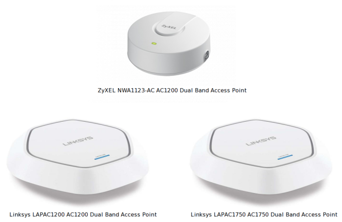
provision of a robust and flexible management interface. We covered the launch of the Ubiquiti UniFi 3.0 and Xirrus XR620 earlier this year.
Traditional consumer Wi-Fi vendors have also started targeting offerings towards this expanding market segment recently. Coinciding with Interop 2014, we have Linksys launching two and ZyXEL officially launching one 802.11ac access point targeting business users. The Linksys LAPAC1200 is a 2x2 design, while the LAPAC1750 is a 3x3 one. The ZyXEL NWA1123-AC is a 2x2 design. All three devices are ceiling-mount units which are dual-band capable and support Power-over-Ethernet (PoE) to eliminate extra power connectors. As applicable to business users, we have support for multiple SSIDs, Layer-2 isolation, specific security features including 802.1X RADIUS authentication, MAC-based ACL etc.
The ZyXEL AP is based on the Qualcomm Atheros AR9342 CPU with a QCA9882 radio. It includes support for transmit beamforming (TxBF) and can have up to 128 wireless clients (64 per radio).
All three devices can operate as either stand-alone APs or repeaters. While the ZyXEL NWA1123-AC retails for a MSRP of $199, the Linksys LAPAC1200 and LAPAC1750 come in at $330 and $380 respectively. Small businesses / SOHO operations looking for a complete system would do well to combine the APs (and any surveillance cameras) with one of the sub-$250 fanless PoE+ switches from either vendor. ZyXEL has the GS1900-8HP GbE 8 Port PoE+ Web Managed Switch while Linksys has the LGS308P 8-Port Smart Gigabit PoE+ Switch in its portfolio. Both of them are fanless and support the latest 802.3at (PoE+) standard with a 70 W power budget.
More...


 Quote
QuoteThread Information
Users Browsing this Thread
There are currently 9 users browsing this thread. (0 members and 9 guests)


Bookmarks