

Results 4,201 to 4,210 of 12096
Thread: Anandtech News
-
08-14-14, 06:30 PM #4201
Anandtech: Isolated Internet Outages Caused By BGP Spike
The day was Tuesday, August 12th 2014. I arrived home, only to find an almost unusable internet situation in my home. Some sites such as AnandTech and Google worked fine, but large swaths of the internet such as Microsoft, Netflix, and many other sites were unreachable. As I run my own DNS servers, I assumed it was a DNS issue, however a couple of ICMP commands later and it was clear that this was a much larger issue than just something affecting my household.
Two days later, and there is a pretty clear understanding of what happened. Older Cisco core internet routers with a default configuration only allowed for a maximum 512k routes for their Border Gateway Protocol (BGP) tables. With the internet always growing, the number of routes surpassed that number briefly on Tuesday, which caused many core routers to be unable to route traffic.
BGP is not something that is discussed very much, due to the average person never needing to worry about it, but it is one of the most used and most important protocols on the internet. The worst part of the outage was that it was known well in advance that this would be an issue, yet it still happened.
Let us dig into the root cause. Most of us have a home network of some sort, with a router, and maybe a dozen or so devices on the network. We connect to an internet service provider through (generally) a modem. When devices on your local network want to talk to other devices on your network, they do so by sending packets upstream to the switch (which is in most cases part of the router) and then the switch forwards the packet to the correct port where the other device is connected. If the second device is not on the local network, the packets get sent to the default gateway which then forwards them upstream to the ISP. At the ISP level, in simple terms, it works very similarly to your LAN. The packet comes in to the ISP network, and if the IP address is something that is in the ISP’s network, it gets routed there, but if it is something on the internet, the packet is forwarded. The big difference though is that an ISP does not have a single default gateway, but instead connects to several internet backbones. The method in which internet packages are routed is based on the Border Gateway Protocol. The BGP contains a table of IP subnets, and lists which ports to transfer traffic based on rules and paths laid out by the network administrator. For instance, if you want to connect to Google to check your Gmail, your computer will send a TCP connection to 173.194.33.111 (or another address as determined by your DNS settings and location). Your ISP will receive this packet, and send the packet to the correct port to an outbound part of the internet which is closer to the subnet that the address is in. If you then want to connect to Anandtech.com, the packet will be sent to 192.65.241.100, and the BGP protocol of the ISP router will then send to possibly a different port. This continues upstream from core router to core router until the packet reaches the destination subnet, where it is then sent to the web server.
With the BGP tables being overfilled on certain routers in the chain, packets send to specific routers would then be dropped at some point in the chain, meaning you would not have any service.
The actual specifics of what happened seemed to be that Verizon unintentionally added approximately 15,000 /24 routes into the global routing table. These prefixes were supposed to be aggregated, but this didn’t happen, and as such, the total number of subnet prefixes in the table spiked. Verizon fixed the mistake quickly, but it still caused many routers to fail.
Although you could be quick to jump and blame Verizon for the outage, it has to be noted that Cisco issued a warning to customers explaining that the memory which is allocated for the BGP table would be very close to being full, and gave specific instructions on how to correct it. This warning came several months ago. Unfortunately not all customers of Cisco heeded or received the warning, which caused the brief spike to cripple parts of the internet.
Newer Cisco routers were not affected, because the default configuration for the TCAM memory which is designated for the BGP table allows for more than 512,000 entries. Older routers from Cisco have enough physical memory for up to 1,000,000 entries, assuming the configuration was changed as outlined by Cisco.
The effects of outages like this can be quite potent on the internet economy, with several online services being unavailable for large parts of the day. However this outage doesn’t need to happen again, even though the steady state number of entries in the BGP table will likely exceed magic 512,000 number again. Hopefully with this brief outage, lessons can be learned, and equipment can be re-configured or upgraded which will prevent this particular issue from rearing its head again in the future.
Sources
DSLReports
Renesys
BGPMon
More...
-
08-15-14, 05:31 AM #4202
Anandtech: Intel Demonstrates Direct3D 12 Performance and Power Improvements
Since the introduction of Direct3D 12 and other low-level graphics APIs, the bulk of our focus has been on the high end. One of the most immediate benefits to these new APIs is their ability to better scale out with multiple threads and alleviate CPU bottlenecking, which has been a growing problem over the years due to GPU performance gains outpacing CPU performance gains.
However at the opposite end of the spectrum and away from the performance benefits are the efficiency benefits, and those are gains that haven’t been covered nearly as well. With that subject in mind, Intel is doing just that this week at SIGGRAPH 2014, where the company is showcasing both the performance and efficiency gains from Direct3D 12 on their hardware.
When it comes to power efficiency Intel stands to be among the biggest beneficiaries of Direct3D 12 due to the fact that they exclusvely ship their GPUs as part of an integrated CPU/GPU product. Because the GPU and CPU portions of their chips share a thermal and power budget, by reducing the software/CPU overhead of Direct3D, Intel can offer both improved performance and power usage with the exact same silicon in the same thermal environment. With Intel's recent focus on power consumption, mobile form factors, and chips like Core M, Direct3D 12 is an obvious boon to Intel.
Intel wisely demonstrated this improvement using a modern low-power mobile device: the Microsoft Surface Pro 3. For this demo Intel is using the Core i5-4300U version, Microsoft’s middle of the road model that clocks up to 2.9GHz on the CPU and features one of Intel’s HD 4400 GPUs, with a maximum GPU clockspeed of 1.1GHz. In our testing, we found the Surface Pro 3 to be thermally constrained – throttling when met with a medium to long duration GPU task. Broadwell should go a long way to improve the situation, and so should Direct3D 12 for current and future Intel devices.
To demonstrate the benefits of Direct3D 12, Intel put together a tech demo that renders 50,000 unique asteroid objects floating in space. The demo can operate in maximum performance mode with the frame rate unrestricted, as well as a fixed frame rate mode to limit CPU and GPU utilization in order to reduce power consumption. The demo can also dynamically switch between making Direct3D 11 and Direct3D 12 API calls. Additionally, an overlay shows power consumption of both the CPU and GPU portions of the Intel processor.
Intel states this demo data was taken after steady-state thermals were reached.
In the performance mode, Direct3D 11 reaches 19 frames per second and the power consumption is roughly evenly split between CPU and GPU. Confirming that while this is a graphical demo, there is significant CPU activity and overhead from handling so many draw calls.
After dynamically switching to Direct3D 12 while in performance mode, the frames per second jumps nearly 75% to 33fps and the power consumption split goes from 50/50 (CPU/GPU) to 25/75. The lower CPU overhead of making Direct3D 12 API calls versus Direct3D 11 API calls allows Intel's processor to maintain its thermal profile but shift more of its power budget to the GPU, improving performance.
Finally, in the power efficiency focused fixed frame rate mode, switching between Direct3D 11 and 12 slightly reduces GPU power consumption but dramatically reduces CPU power consumption, all while maintaining the same 19fps frame rate. Intel's data shows a 50% total power reduction, virtually all of which comes from CPU power savings. As Intel notes, not only do they save power from having to do less work overall, but they also save power because they are able to better distribute the workload over more CPU cores, allowing each core in turn to run at a lower clockspeed and voltage for greater power efficiency.
To put these numbers in perspective, a 50% reduction in power consumption is about what we would see from a new silicon process (i.e. moving from 22nm to 14nm), so to achieve such a reduction in consumption with software alone is a very significant result and a feather in Microsoft’s cap for Direct3D 12. If this carries over to games and applications when DirectX 12 launches in Q4 2015, it could help usher in a new era of mobile gaming and high end graphics. It is not often we see such a substantial power and performance improvement from a software update.
Source: Intel, Microsoft
More...
-
08-15-14, 05:31 AM #4203
Anandtech: Corsair Carbide Air 240 Case Review
With compact cases and SSFs being all the rage nowadays, today Corsair is launching the Carbide Air 240, a cubic Micro-ATX case designed to fit powerful PC hardware. As the name suggests, it is based on the design of the Full-ATX Carbide Air 540 that released last year. Can the smaller version make the same impact impact as its larger, older brother? We will find out in this review.
More...
-
08-15-14, 06:33 AM #4204
Anandtech: ASRock Shows X99 Micro-ATX: The X99M Killer
One of the problems of Intel’s high end desktop platforms is size: the sockets are large, and all the DRAM slots take up a fair amount of space. Couple this with the PCIe lane potential of the CPU, then restricting the motherboard size smaller than ATX limits the number of features and multi-PCIe capabilities afforded by the platform. Nonetheless we saw a couple of motherboards for X79 move down to the micro-ATX size, as well as a few system designer builds that offered other sizes. In that vein, ASRock is moving from its X79 Extreme4-M (our review) and sent us pictures of the upcoming X99M Killer.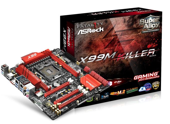
One thing that a micro-ATX layout does is free up some of the PCIe lanes for extra controllers. The X99M Killer will have ASRock’s Ultra M.2, giving PCIe 3.0 x4 bandwidth for devices up to 22110. Being part of ASRock’s Killer range we get an E2200 series network interface, which also incorporates an EM shield similar to the Purity Sound 2 upgraded audio. The Killer NIC is paired with an Intel NIC as well, with the Fatal1ty Mouse Port also appearing.
Due to the size, if any other mATX motherboards are released I would assume that like the X99M Killer there will only be four DDR4 memory slots, and here ASRock have used thinner slots in order to fit the power delivery and other features on board. I count five fan headers on the board, along with ASRock’s HDD Saver connector and ten SATA 6 Gbps ports. I can just about make out that some of these are labelled SATA3_0_1 and some are labelled 5_SATA3_0_1, perhaps indicating the presence of a controller or a hub. There is also a USB 3.0 header on board with power/reset buttons, a two digit debug, two BIOS chips, two USB 2.0 headers, a COM header and additional power to the PCIe slots via s 4-pin molex. We also have an eSATA on the rear panel, with a ClearCMOS button.
We can make out the final PCIe slot as having only four lanes of pins, suggesting an x16/x16/x4 layout. Whether these four lanes are from the CPU or the chipset is unclear, especially with the presence of the PCIe 3.0 M.2 x4 slot in the middle.
The box lists XSplit, indicating a bundling deal with the software, as well as ECC and RDIMM support. I believe the X99M Killer will be due out at launch, or relatively soon after, although ASRock has not released the pricing details yet.
More...
-
08-15-14, 09:30 AM #4205
Anandtech: ASUS Motherboard Division Director: An Interview with Dr Albert Chang
Following our interviews previously with Rod O’Shea at Intel UK, Kris Huang at ASUS and Jackson Hsu at GIGABYTE, I was offered the opportunity to spend some time with Dr Albert Chang, the Senior Division Director in R&D for the entire Motherboard Business Unit at ASUS. The motherboard design and testing facilities span several floors of their headquarters, which we toured during Computex. I would like to thank ASUS and Dr Chang for their time and this opportunity.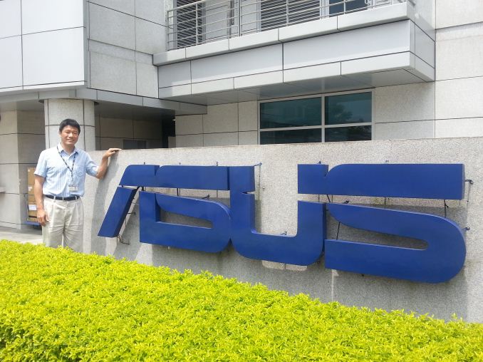
Ian Cutress: Everyone sees a corporation, but there are always interesting people to talk to. Everyone has a back story and it is always interesting to hear how people have risen to where they are. Your business card says ‘Division Director’ – what exactly does a Division Director do?
Albert Chang: I am the ASUS motherboard R&D head, so I have three major teams. One of these is in Taiwan, with two others in China. The team in Taiwan focuses on ROG, with the other two in China for channel motherboards and SI customer designs.
IC: What is your typical day?
AC: Usually I have to review all the projects. We usually have 20-30 projects running at the same time. Being one person it can be hard to review all details, but I have staff that report to me and then I can discuss any problems in case any department needs assistance or approval.
IC: How long have you been in this position at ASUS?
AC: I have been Division Director for two years and at ASUS since 2002 straight after finishing my PhD from the National Taiwan University. I started as an engineer, checking datasheets and layouts. At ASUS, as a motherboard engineer, you are the project owner and you have to discuss everything with the Product Manager (layout, engineering) and others like the power and layout engineers. We had to design based on the specification sheets and confirm with layout engineers. I managed a couple of people at that time, and a lot more now!
IC: With regards to your education, what were your courses?
AC: I majored in Electrical Engineering, with a focus on Power Electronics. I finished my PhD at 28 and joined ASUS at that time.
IC: In your position, do you work a ‘9-to-5’, or do you have to come in on weekends?
AC: Sometimes at weekends, especially to have meetings with either North America or Europe, or to fix major issues that rise up. I have a family, but they are not too keen on me coming in on weekends! I sometimes have to buy cake or a gift when I get home!
IC: As Division Director, do you get final say on what happens with the motherboards?
AC: On the engineering side, yes, but there are also the firmware and software teams.
IC: Does the sales department ask you to do certain designs?
AC: All requests of that nature go through the product managers, who relay information through to R&D. So for ROG, Kris Huang (we interviewed him in 2012) is the product manager.
IC: How does user demand get fed back into designs?
AC: Typically I will speak to our product managers (both sales and marketing), or our technical marketing teams directly who monitor the forums and produce reports about user experience. Sometimes I like to hear direct from the teams gathering this information and interacting directly with the users, especially with our major regions such as North America. We have to look at the global market, and decide on ideas or features that benefit everyone.
IC: In terms of ideas for future platforms, who gets them/where do they come from?
AC: We initially look at our competitors’ product, to see which direction they are going, and also examine media reviews to see which options they like or want to see improved. Features like the OC Panel come from the engineers in the ROG team. Because I am only one person, we encourage every engineer to share any ideas in meetings so we can discuss them. There are multiple streams – some from in-house engineers, some from feedback, and some from product managers.
IC: What percentage of users need to request a feature before it is implemented?
AC: If a request comes up repeatedly, we evaluate the idea based on relevance and increased cost on the motherboards. For example, adding DC and PWM fan control on the motherboard came from a core group of users that wanted to be able to have the control. It also helps if the media notice the new feature as well, and can help relay this to other users.
IC: How is market research for new ideas performed?
AC: We have the forums, but also social media plays a role. We sometimes give users a choice between two features (for example, audio codec A or B), and even if we only get 40 or so responses, we weigh up the percentages. The product managers for each region that understand their customers can also have input on new ideas.
IC: At what point in the product cycle to you start looking at the next generation of motherboards? If you released a motherboard today, how far back would you have to start planning for it?
AC: At least nine months, in terms of the start point in thinking about what we want to do.
In the first three months, we will start analyzing the new major features for the CPU and chipset generation from the CPU manufacturer guidelines, paying attention to the differences to the old platform. We also look over bugs from the old generation, or ideas that we could not implement in the last generation. We also check the competitors’ products for the last generation, including the feedback from their users. At that point we talk to the major IC vendors (Renesas, ASMedia, Qualcomm Atheros) for their plans and roadmaps for the next 6-9 months so we have the latest for launch.
In month four, we finalize the segmentation for the product line, including form factor, and start the circuit design. We also work with Intel with early samples which can have a lot of bugs, so we report back to Intel in terms of processor and chipset evaluation for their PVT/first stepping samples. The microcode gets revised several times. We take 4-6 weeks for the circuit design before we get the first motherboards ready for testing, and by this time we have those Intel CPU samples for testing.
We build 60-100 boards for a sample run when the design is coming together, for validation, reliability, checking the power and everything. This includes the aging tests, such as high temperature stress testing. Typically our rule is a 12 hour test at this point, and if there are any errors in those twelve hours for these pre-production models, we then have to check it. The process of testing, changing and retesting can take up to three months to catch any bugs. At every change or iteration due to hardware bugs, we need to retest and revalidate.
At 7.5 months, we are at PVT stage before mass production. We ensure all the third party IC orders are in and will work with the motherboards. We work with factories in China for mass production and place our orders with them to build our motherboards. We have to check the production quality of the factory output. We typically send project managers or leaders to manage production and work with the factories in terms of managing the schedules as well as quantity.
Mass production starts about a month before launch, and in that time we also distribute hardware around the world. This also involves the sales teams talking to their local regional SIs, as well as inviting media to preview events. Typically the media receive samples from the first mass production batch.
IC: So by the timeline, users and media need to start asking for certain features around 5-8 months before a launch! We normally do not know that there is a launch until it almost happens.
AC: Yes, sometimes changes late in the day are difficult to do. But we keep the ideas generated throughout the generation and see what we can apply next time around. But for example, with the memory design, we do not always follow Intel guidelines. We have our own memory team and do a lot of simulations based on layout and tracing to find the best way to get the most out of the memory. We want to better than the reference design, and ROG team is the best at pushing the new designs. So if we want the best memory records, we need to have the best design.
IC: How long is the lead time, from placing an order to receiving stock, for the controllers?
AC: For the testing motherboards, we usually can get stock within a week or two. For the mass production, if it works in our design, it is more like 4-6 weeks. This includes other things like the PCB, which can sometimes be over 6 weeks.
IC: When do you start designing the additional materials (box, foam inserts, manuals)?
AC: We go through a lot of internal discussions, and there are a lot of revisions when it comes down to design. The design teams talk to sales and see what the competition are doing, but early design talks can be 6-9 months away from a launch, as the tracing teams are designing the motherboards.
IC: When you mention 60-100 motherboards for a sample run, is that 100 motherboards for every SKU? So for the seven Z97 channel motherboards, you would have almost 700 samples?
AC: Yes, every SKU, of course!
IC: In terms of product production goals, what would be your main goals in the next twelve months?
AC: In the first two months of a launch, we check to see if our features meet the customers’ needs. After that, we start to study the next generation. For me, I hope that each generation we can make the boards that everyone likes, because this is my product line at ASUS.
IC: How about the next five years?
AC: I will still be at ASUS, and I want to help expand PC applications in the home. Our chairman Jonney Shih has mentioned at Computex that this is a primary focus for ASUS.
IC: What do you think are the most important innovations that ASUS has created in the motherboard segment recently?
AC: Too many, cannot pick! Our ROG features span so many projects, for example. We have made our overclocking features easier to use than before, especially with automatic overclocking in BIOS and software, but also with the ROG OC Panel. Not many users know how to overclock, so we want to make it easier with our Auto Tuning, especially with voltages and stress testing. But we also cater for the extreme tweakers that use ROG.
IC: What element or feature from the ASUS Motherboard Business Unit do you think users need to know more about?
AC: We use separate components on the motherboard to help manage features like overclocking, but not many users know that we also do the same for other features like power saving. This is separate from the CPU and chipset, for example our Dual Intelligent Processors design. This is our own custom designed chip for our motherboards, not something off the shelf, which users may not realize.
IC: Do you see a gap in the market that ASUS or the Motherboard Business Unit should move in to?
AC: Gaming and small form factor markets are growing, and other ultra-small form factors like the NUC and Chromebox are interesting. We announced the GR8 at Computex, which is a combination of this for around 1.5 liter of volume. The sub 1-liter market should be a focus in the future.
IC: A question I like to pose in our interviews – what advice would you give to a high school student wanting to work for ASUS or to be in the position where you are today?
AC: The best thing is to be interested in electronics and computers. An engineer has to be familiar with this industry, especially the DIY market. Part of being an engineer is building PCs every day, up to 20-30. At the start of my career I had to build every machine by myself. At university, studying electronics or electronic engineering is vital. Out of the ~100 engineers on the fifth floor of HQ, the motherboard engineering floor, three or four have PhDs, most (70%+) have a Master’s and the rest have a Bachelor’s degree.
IC: If you were not working at ASUS, what would you be doing now? Would you still be in engineering?
AC: I would enjoy trying my hand at marketing! I like to promote the products.
IC: To what extent do you look at your competitors’ products?
AC: Our competitors are very aggressive and focused. We use our testing and validation processes on their products to see if they qualify.
IC: What has been your best day working at ASUS? Is there one specific moment that stands out compared to any other?
AC: When I started at ASUS, there was (still is) a philosophy of doing it right first time. Any engineer that produced a product that did not need a second revision (or a revision 1.01) who achieved this got a small bonus, something like 10000NT$ (~$300). In the R&D team, I was the first person to get this award, and it was in my second project ever at ASUS, just after I had started. Normally there might be some layout bug, or signaling bug, but I was very pleased to get it right first time so early in my career.
IC: Do you remember the model name?
It was an AMD motherboard, the SK8V. (We actually reviewed this, back in 2003)
Many thanks to Dr Chang for his time!
More...
-
08-15-14, 02:30 PM #4206
Anandtech: GIGABYTE AM1M-S2H Review: What Can $35 Get You?
While most of the time enthusiasts are playing around with the latest and greatest, the cheaper low performance platforms are usually the high volume movers. As we explained in our Kabini review, AMD has taken the unusual step of producing an upgradable platform for as little as $74. The motherboards for the AM1 Kabini platform range from $31 to $47, and today we are reviewing the GIGABYTE AM1M-S2H which retails at $35.
More...
-
08-18-14, 05:33 AM #4207
Anandtech: Browser Face-Off: Chrome 37 Beta Battery Life Revisited
Last week we posted our Browser Face-Off: Battery Life Explored 2014, where the battery run down times of Firefox 31, IE11 Desktop, IE11 Modern, Chrome 36, and Chrome 37 beta were tested on Windows. We used GUI automation to open browsers, tabs, and visit websites to simulate a real user in a light reading pattern. The article answered a lot of questions about popular browser battery life on Windows, but it raised additional questions as well.
Chrome 36 tested with the best battery life, but was the only browser that did not render correctly at 3200x1800 due to lack of HiDPI support. In the Chrome 37 beta, HiDPI support improved rendering but also took a 25% dive in battery life tying it for last place. However, the Chrome 37 beta includes more changes than just HiDPI support (along with some debugging code), so was the battery life penalty from the now-native 3200x1800 rendering or was it something else? After a few more days of testing at 1600x900 with 100% DPI scaling, we can narrow in on an answer.
When both Chrome 36 and Chrome 37 beta natively render at 1600x900 there is less than 3% difference in battery life. Two tests of each browser were performed and the results averaged. The variation between runs was only 1%. Looking at our previous numbers of Chome 36 and 37 beta on the HiDPI setting of 3200x1800 and 200% scaling, the situation is entirely different.
I've added an asterisk here (and clarified the same text on the original article) to indicate Chrome 36 isn't actually rendering at 3200x1800, but rather at 1600x900 and relying on Windows DPI Virtualization to scale up to 3200x1800.
Looking at the numbers, we there's some good news and some bad news. The good news is that Chrome 37's new features likely won't hurt the battery life of current users. If you are using Chrome now, you are probably not using a HiDPI display due to the existing blurry rendering. For these users, the pending Chrome 37 upgrade has no significant impact on battery life. The bad news is that if you have been avoiding Chrome due to its HiDPI rending issues, Chrome 37 resolves those issues but also appears to provide worse battery efficiency compared to Internet Explorer. On our XPS 15 that equated to about an hour less of mobility.
Given that this is the first version of Chrome to properly support HiDPI, it's entirely possible – even likely – that there are many opportunities to further optimize the algorithms and hopefully return battery life at least close to Chome 36 levels. A slight dip in battery life is expected as it takes more work to render a 3200x1800 image compared to a 1600x900 image, but a 20% drop seems rather extreme. We'll have to see what future updates bring, but hopefully by noting the discrepancy it will encourage developers to better tune performance.
More...
-
08-18-14, 06:30 AM #4208
Anandtech: FMS 2014: SanDisk ULLtraDIMM to Ship in Supermicro's Servers
We are running a bit late with our Flash Memory Summit coverage as I did not get back from the US until last Friday, but I still wanted to cover the most interesting tidbits of the show. ULLtraDIMM (Ultra Low Latency DIMM) was initially launched by SMART Storage a year ago but SanDisk acquired the company shortly after, which made ULLtraDIMM a part of SanDisk's product portfolio.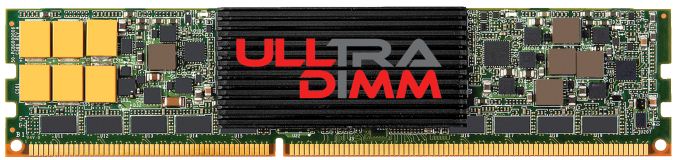
The ULLtraDIMM was developed in partnership with Diablo Technologies and it is an enterprise SSD that connects to the DDR3 interface instead of the traditional SATA/SAS and PCIe interfaces. IBM was the first to partner with the two to ship the ULLtraDIMM in servers, but at this year's show SanDisk announced that Supermicro will be joining as the second partner to use ULLtraDIMM SSDs. More specifically Supermicro will be shipping ULLtraDIMM in its Green SuperServer and SuperStorage platforms and availability is scheduled for Q4 this year.
We have not covered the ULLtraDIMM before, so I figured I would provide a quick overview of the product as well. Hardware wise the ULLtraDIMM consists of two Marvell 88SS9187 SATA 6Gbps controllers, which are configured in an array using a custom chip with a Diablo Technologies label, which I presume is also the secret behind DDR3 compatibility. ULLtraDIMM supports F.R.A.M.E. (Flexible Redundant Array of Memory Elements) that utilizes parity to protect against page/block/die level failures, which is SanDisk's answer to SandForce's RAISE and Micron's RAIN. Power loss protection is supported as well and is provided by an array of capacitors.SanDisk ULLtraDIMM Specifications Capacities 200GB & 400GB Controller 2x Marvell 88SS9187 NAND SanDisk 19nm MLC Sequential Read 1,000MB/s Sequential Write 760MB/s 4KB Random Read 150K IOPS 4KB Random Write 65K IOPS Read Latency 150 µsec Write Latency < 5 µsec Endurance 10/25 DWPD (random/sequential) Warranty Five years
The benefit of using a DDR3 interface instead of SATA/SAS or PCIe is lower latency because the SSDs sit closer to the CPU. The memory interface has also been designed with parallelism in mind and can thus take greater advantage of multiple drives without sacrificing performance or latency. SanDisk claims write latency of less then five microseconds, which is lower than what even PCIe SSDs offer (e.g. Intel SSD DC P3700 is rated at 20µs).
Unfortunately there are no third party benchmarks for the ULLtraDIMM so it is hard to say how it really stacks up against PCIe SSDs, but the concept is definitely intriguing. In the end, NAND flash is memory and putting it on the DDR3 interface is logical, even though NAND is not as fast as DRAM. NVMe is designed to make PCIe more flash friendly but there are still some intensive workloads that should benefit from the lower latency of the DDR3 interface. Hopefully we will be able to get a review sample soon, so we can put ULLtraDIMM through our own tests and see how it really compares with the competition.
More...
-
08-18-14, 08:32 AM #4209
Anandtech: FMS 2014: HGST Announces FlashMAX III PCIe SSDs
Continuing with our Flash Memory Summit coverage, HGST announced their FlashMAX III enterprise SSD, which is the first fruit of HGST's Virident acquistion and continues Virident's FlashMAX brand. The FlashMAX III will come in half-height, half-length form factor and will be available in capacities of 1100GB, 1650GB and 2200GB. The controller is an FPGA-based 32-channel design with a PCIe 3.0 x8 interface, but there is no NVMe support since the FlashMAX III builds on the same architecture as the previous generation FlashMAX II._575px.png)
The maximum throughput seems a bit low for a design that uses up eight PCIe 3.0 lanes since 2.7GB/s should be achievable with just four PCIe 3.0 lanes. Obviously performance scaling is not that simple but for example Samsung's XS1715 (which we will be reviewing soon!) is rated at up to 3.0GB/s while only consuming four PCIe 3.0 lanes. Using less PCIe lanes allows for more drives to be delpoyed as the amount of PCIe lanes is always rather limited.HGST FlashMAX III Specifications Capacity 1100GB 1650GB 2200GB Form Factor Half-Height, Half-Length (HH-HL) Interface PCIe 3.0 x8 Controller 32-channel FPGA based NAND Micron 20nm 64Gbit MLC Sequential Read 2.7GB/s 2.0GB/s 2.7GB/s Sequential Write 1.4GB/s 1.0GB/s 1.4GB/s 4KB Random Read 549K IOPS 409K IOPS 531K IOPS 4KB Random Write 53K IOPS 30K IOPS 59K IOPS 4KB 70/30 Random Read/Write 195K IOPS 145K IOPS 200K IOPS Write Latency < 30 µsec Max Power 25 watts Endurance 2 DWPD Warranty Five years
The 1650GB model is even slower due to the fact that it utilizes less NAND channels because it is a middle capacity. Basically, the 1100GB and 2200GB models have the same number of NAND packages, with the 2200GB model having twice as much NAND per package; the 1650GB model uses the higher capacity packages but doesn't fully populate the board. HGST told us that they are just testing the water to see if there is demand for something in between 1100GB and 2200GB.
The FlashMAX III also supports Virident Flash-management with Adaptive Shceduling (vFAS), which is a fancy name for Virident's storage driver. vFAS presents the FlashMAX as a single volume block device to the OS, meaning that no additional storage protocols or controllers are needed, whereas some drives just use a RAID controller or need software RAID solutions to be configured into an array. Additionally vFAS handles NAND management by doing wear-leveling, garbage collection, data path protection, NAND-level parity, ECC, and more.
The FlashMAX III is currently being qualified by select OEMs and will ship later in this quarter.
More...
-
08-18-14, 09:30 AM #4210
Anandtech: NAS Units as VM Hosts: QNAP's Virtualization Station Explored
Virtualization has been around since the 1960s, but it has emerged as a hot topic over the last decade or so. Despite the rising popularity, its applications have been mostly restricted to enterprise use. Hardware-assisted virtualization features (AMD-V, VT-x and VT-d, for example) have been slowly making their way into the lower end x86 parts, thereby enabling low-cost virtualization platforms. QNAP is, to our knowledge, the only NAS vendor to offer a virtualization platform (using the Virtualization Station package for QTS) with some of their units. Read on to find out how it works and the impact it has on regular performance.
More...


 Quote
QuoteThread Information
Users Browsing this Thread
There are currently 9 users browsing this thread. (0 members and 9 guests)


Bookmarks