

Results 4,761 to 4,770 of 12094
Thread: Anandtech News
-
02-23-15, 07:00 PM #4761
Anandtech: AMD at ISSCC 2015: Carrizo and Excavator Details
AMD is using the International Solid-State Circuits Conference this week to present a paper and announce some interesting developments regarding the next iteration of the Bulldozer architecture, codenamed ‘Excavator’, as well as other details regarding the CPU range that it will be placed in called ‘Carrizo’.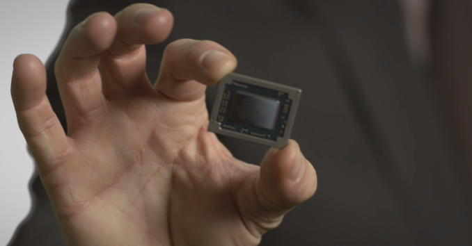
At the tail end of 2014 we reported on Carrizo and AMD’s announcement for its next generation of APUs, and more recently the discussion surrounding Carrizo not coming to desktop. In those announcements AMD revealed that Carrizo will be aimed at the laptop and notebook community first and foremost, a first for the company as previous APU designs have been aimed at both the desktop and mobile markets.
From a hardware standpoint, Carrizo will be combining a number of Excavator modules, AMD’s R-Series GCN GPUs, and the chipset/Fusion Controller Hub into a single package, bringing with it full HSA compatibility, TrueAudio, and ARM Trustzone compatibility. As with Kaveri before it, Carrizo will be built on Global Foundries’ 28nm Super High Performance (28SHP) node, making Carrizo a pure architecture upgrade without any manufacturing changes. Today’s ISSCC paper in turn builds on these revelations, showing some of the data from AMD’s internal silicon testing.
AMD’s presentation confirms that the new Excavator cores are low power optimized rather than desktop optimized. Support for Mantle and DirectX 12 should go without saying, and Dual Graphics support is something AMD has been working on for a number of generations. The next point is interesting from my perspective:
“Single-chip integration of the APU and the Southbridge onto a single die”
In our pre-briefing call, AMD confirmed that the south bridge/FCH is no longer a separate chip, and is being moved on to the CPU from its previously separate package. In fact not only is the south bridge going to part of the CPU with Carrizo, but it's being fully integrated into the APU die itself. This is a first for AMD, and even Intel by comparison still uses two separate dies on the same package for their similar Broadwell-Y/U processors. As a result, AMD explained, this advances the soutb bridge from the older 65nm/45nm processes to 28nm and 28SHP, reducing power consumption and operating voltage. It also allows the APU to accurately control power gating, further saving power, and reduces the length of HyperTransport interconnects between the APU and the I/O. On the flip side, it does move the soutb bridge's power consumption onto the APU, as well as the extra transistors it would otherwise occupy. This is explained in detail below.
The key element to Excavator’s design is a reduction in die area. Fundamentally everything is the same in terms of operation compared to Kaveri, but the internal units such as the FP scheduler and cache control have been re-engineered to take up less room on the same 28nm SHP process node. It seems a little odd applying a ‘high-density’ design to a ‘high-performance’ process node, but AMD is stating that part of this has been driven by the GPU team sharing its experiences and knowledge of small, efficient die components with the CPU team, allowing the lessons learned there to benefit AMD's CPU designs. This is combined with a "GPU-oriented" design stack on the CPU, which AMD is showing provides significant power savings at the same frequency, or higher frequency at the same power.
The high density, power optimized design also plays a role in the GPU segment of Carrizo, offering lower leakage at high voltages as well as allowing a full 8 GCN core design at 20W. This is an improvement from Kaveri, which due to power consumption only allowed a 6 GCN design at the same power without compromising performance.
AMD revealed Voltage Adaptive Operation back with Kaveri, and it makes a reappearance in Carrizo with its next iteration. The principle here is that with a high noise line, the excess voltage will cause power to rise. If the system reduces the frequency of the CPU during high noise/voltage segments - as power is proportional to voltage squared - power consumption will be reduced and then frequency can be restored when noise returns to normal. This happens inside the CPU over nanoseconds, resulting in no serious performance loss but it helps keep the power consumption of the APU down. In the case of Carrizo, AMD is quoting a 10-20% reduction in power consumption versus what a theoretical Carrizo would look like without this technology.
Another new addition to Excavator comes in the form of Adaptive Voltage-Frequency Scaling modules. Carrizo uses 10 in each Excavator ‘core’, and these modules can adjust the frequency and voltage of individual components depending on power requirements, temperature and other external factors in order to improve either performance, power consumption, or efficiency. With this in mind, AMD is claiming a 29% frequency increase at 10W, or if frequency is held constant then there is a 40-50% power decrease at the same 10W. At 20W, as the graph shows, there is almost no difference between the two, indicating that Excavator is truly built for lower TDP devices.
AMD is also presenting news on improvements to their ability to quickly enter and exit sleep states. With Excavator, AMD can now go from a sub-50mW S0i3 state to an active state in under a second. This should allow Carrizo devices to quickly reach and better sustain near-standby power levels, improving idle and low-load power consumption. As shown in the slide, at the S0i3 state only the ACP, PCH, and a small I/O segment are still active, while the rest of the device is completely power gated.
Meanwhile AMD is also once again showing off their technology timeline to illustrate their progress in implementing new technologies over the years. We confirmed that an interesting feature, inter-frame power gating, is active in Carrizo. This in a nutshell allows the GPU to go to a low frequency mode frame buffers are full. Though only a few milliseconds of power savings at a time, over time this can add up to larger increases battery life.
Wrapping up the hardware aspects of their ISSCC presentation, AMD is also disclosing the die size and transistor counts for Carrizo. Whereas Kaveri weighed in at 2.3 billion transistors in a 245mm2 die, Carrizo will come in at a much larger 3.1 billion transistors in a 250mm2 die. This a significant increase in transistor density for AMD, with Carrizo packing in 29% more transistors for only a marginal increase in die size. Though AMD is not explaining where all of the transistor increases come from at this time, part of the increase comes from the Southbridge/FCH being moved on-die, which AMD tells us will take up 5.5% of Carrizo's die. As for the Excavator cores themselves, AMD is starting that they consume 40% less power and take up 23% less die area, thanks to the combination of transistor density improvements, AVFS technology, and bringing the FCH on-die.
Moving on, although AMD's ISSCC presentation is not going to be diving deep into the Excavator architecture, AMD is claiming that Excavator will also bring with it a 5% IPC boost. We understand that this increase in IPC comes from a doubling of the L1 data cache from 64KB to 128KB, as well as further payoffs from the power improvements. Meanwhile on the fixed-function side of matters, Carrizo will be introducing a full H.265 hardware decoder. This is the first AMD part (CPU or GPU) to offer any kind of hardware support for H.265 decoding, and in the process it will be the first x86 CPU/APU to offer full hardware decode capabilities, as Intel still relies on a hybrid decode approach at this time.
Finally, AMD is also rolling out some new Heterogeneous System Architecture (HSA) functionality as part of Carrizo. HSA is seen as one of the next key factors in personal computing over the next decade. We have seen an almost ubiquitous shift in recent years towards almost every consumer processor having on-die graphics, and the ability to optimize a workload for each part of the system improves the experience. AMD has been riding this wave, announcing Kaveri as ‘HSA Ready’ and now Carrizo as ‘HSA Compliant’, fully adhering to HSA 1.0 specifications. At the moment the biggest benchmark showing off this power is PCMark, something AMD likes to promote. With regards the difference between HSA Ready and Compliant, I asked AMD what made Kaveri different in that regard. The answer was straightforward enough: Carrizo is able to perform GPU context switching, allowing a GPU state-save and state-restore, something Kaveri is unable to do and offering a solid hint that Carrizo's GPU is based on AMD's GCN 1.2 architecture.
Wrapping things up, the combination of a 5% IPC boost and 40% power savings means that AMD has a range of options for Carrizo parts, picking between increased clockspeeds at the same power levels or holding clockspeeds constant for a larger battery life gain. We expect that actual retail parts will be somewhere in the middle, as the graphs in the slides indicate that best efficiency occurs around the 10W scenario.
We did ask about absolute design numbers regarding battery life, processor frequencies and time to market. As expected, AMD is keeping its cards close to its chest, especially in a more academic environment such as ISSCC. At this point in time we were told that Carrizo is expected to come to market within Q2. With Computex taking place towards the end of Q2, this should mean that a number of Carrizo devices will either be on the market or at least on display for us to examine.
More...
-
02-23-15, 10:00 PM #4762
Anandtech: Valve to Showcase SteamVR Hardware, Steam Machines, & More at GDC 2015
Typically we don’t do announcements of announcements. However in Valve’s case it’s not entirely clear if there’s actually going to be an announcement at GDC, so let's take a quick look at what Valve is up to.
Valve has put out a press release today announcing that the company will be at GDC and will be showing off several hardware initiatives at GDC. Among them will be the final version of the Steam Controller, more Steam Machines, “new living room devices”, and the eye-catcher of the group, a new hardware system Valve is calling SteamVR.
Valve of course has been working on all of those initiatives for some time now, very publicly in the case of the Steam Machines and Steam Controller, and much more quietly on SteamVR. In the case of Steam Machines and Steam controller, 2014 came and left without a release of either, leaving some ambiguity over the state of those projects. Meanwhile we know that Valve has been experimenting with VR for several years now, and although Valve’s press release doesn’t offer any details on what SteamVR may be, they have a GDC programming session scheduled whose description offers a bit more insight:
Valve has been creating advanced prototype VR HMD's since mid-2013 that are more advanced than other developers currently have access to, and this head start has allowed us to gain a ton of VR-specific rendering knowledge that we'd like to share with developers who are actively working on VR or plan to in the near future.This may mean that Valve is working on their own VR headset. Then again it may be an ecosystem/specification/initiative similar to Steam Machines.
Anyhow, for the moment it’s unknown whether SteamVR will be revealed to the public at GDC. Valve already held a press-free event in Washington in January, and their GDC press release does not include any details about a session/event where SteamVR would be announced. Instead Valve is inviting only “developers and publishers” to sign up for demos of SteamVR at GDC through the Steam Universe page, in which case this may be all we hear on SteamVR for now.
February 23, 2015 - Valve will show a family of new Steam devices at next week's Game Developers Conference (GDC) in San Francisco, CA. Products being demonstrated at GDC include Steam Machines with the final Steam Controller, new living room devices, and a previously-unannounced SteamVR hardware system.
Developers and publishers interested in experiencing the new SteamVR hardware may request to schedule a GDC demo at The Steam Universe is expanding.
GDC 2015 will mark the 13th anniversary of Valve's first public announcement of Steam, which has since become the leading platform for PC, Mac, and Linux games and software.
In the last year, Steam added new services and features - including In-Home Streaming, Broadcasting, Music, and user created stores - as it grew to over 125 million active accounts worldwide.
Steam now offers 4500 games, with 400 million pieces of user-generated content contributed by members of the Steam Community.
More...
-
02-24-15, 07:00 AM #4763
Anandtech: ASUS Goes USB 3.1: Motherboards, PCIe Cards and Enclosures Tested
As the motherboard reviewer at AnandTech, I speak to my contacts at the motherboard manufacturers on a regular basis. All the recent talk has had a heavy sprinkling about thoughts, opinions and implementations of USB 3.1. To add to our recent testing, ASUS is today announcing the launch of their USB 3.1 PCIe card along with a variety of motherboard bundles either featuring onboard USB 3.1 or a bundled USB 3.1 card. We stuck the card in the Rampage V Extreme to run the numbers with an ASUS dual mSATA USB 3.1 enclosure.
The ASUS Plan Of Attack
As we expressed in our previous piece, USB 3.1 adoption will take an excruciating long time, especially as USB 3.0 is only now reaching price party with USB 2.0. But as with USB 3.0 we will first start to see USB 3.1 adopted on PCIe cards and extra controllers first on desktops followed by high end laptops before it becomes part of the chipset standard. Even then, with a ubiquity of ports available, it takes time for the devices to appear in the market with sufficient quantity to become cost effective for all but the early adopters.
Nevertheless, motherboard manufacturers want to tackle this head on. As far as we can tell there are a handful of IC manufactures that can provide controllers to be placed in products, but ASMedia are more ready than others to actually sell the components. ASUS' close relationship with ASMedia allows them to approach the market in two different ways - either by an onboard controller or via a bundled PCIe card.
At this point in time, all the implementations from ASUS will be via the Type-A interface. A couple of high end motherboards will be offered with USB 3.1 PCIe cards, while those lower down the stack will be modified for the onboard controller for about a dozen in total. There will be a USB Type-C card released at a later date, available only as a separate purchase.
One tack that ASUS is implemented differently is the color of the USB 3.1 Type-A ports. Standard procedure for USB 2.0 is a black port, with USB 3.0 as blue. This is not a hard and fast rule, as we see red ports on some motherboards for gaming or green ports on the Razer Blade, but as if yet there is no clear definition for USB 3.1. In this instance, ASUS is going with a teal blue to represent USB 3.1, and offers enough contrast from USB 3.0.
The card itself uses the ASMedia ASM1142 controller in a PCIe 2.0 x2 form factor. This should provide the 10 Gbps data rate for the USB 3.1 standard. The Type-A versions will support 900 mA charging at 5V, whereas Type-C will do 3A at 5V, suitable for 15W. In order to get the 100W charging and implement the enhanced power standard, the power delivery delivery has to be built into the power module around the USB 3.1 controller. With PCIe cards this makes more sense, although it would require the card to have an extra power connector (either SATA, molex or PCIe). When the USB 3.1 port is on the rear panel of a motherboard, it makes it more difficult to apply the approach power planes, especially on cheaper motherboards, as well as drawing power directly from the 24-pin ATX and directing the appropriate power around the processor. Thus if we ever see 100W charging on motherboards, PCIe cards might be the way forward.
As part of the testing bundle, ASUS supplied a near-final version of a USB 3.1 storage device. This small form factor uses two 256 GB Samsung 840 EVO mSATA drives in RAID-0 for maximum throughput.
In order to keep the size of the device down, it uses a Type-C connector for data along with a micro-USB for power. This means that the device requires two USB ports in all, which is understandable for a dual mSATA device that requires power but perhaps somewhat limiting for devices with only one USB port. It is unknown if ASUS will sell this enclosure separately at this point.
Both the card and the enclosure are still in development, and we had a difficult time to get it to work. For example, with the Rampage V Extreme and the USB 3.1 card, the enclosure had to be plugged in at power up, with power and data both connected to the card. Without this, the system would not recognize the device or it would enter a speed mode indicative of PCIe 2.0 x1 data transfers eventually ending up in an IO error. Also, our setup did not want to work in USB 2.0 mode at all. But when we installed the right drivers, and booted the system with the cables set up as required, we got great performance. There was a little coil whine during system writes, but as mentioned this device is still in development, and hopefully all these issues can be ironed out.
Unfortunately all the hardware for our previous USB 3.1 testing had to be sent back which means we cannot do a direct comparison due to different enclosures, but it is still interesting to see where the numbers land. ASUS is also touting an updated USB 3.0 Boost as well, dubbed USB 3.1 Boost, to help with transfers. The current state of play with USB transfer speeds is a miasma from XP drivers, base Intel drivers for Windows 7 and then UASP implementations in Windows 8. The basic mode in Windows 7 means that Bulk Only Transfer (BOT) is par for the course:
UASP, or USB Attached SCSI Protocol, allows transfers to occur by multitasking the transfers without the need for constant iterations up and down the stack for each read or write command.
Windows 8 offers a good version of UASP, however ASUS’ customized driver for Intel and ASMedia based ports goes one better through optimization. Normally such processes sacrifice latency for peak speeds, although we are rarely latency limited with a USB drive. Windows 7 also gets a similar driver, which represents a bigger boost from the base driver there.
Test SetupThe ResultsTest Setup Processor Intel Core i7-5960X ES
8 Cores, 16 Threads, 3.0 GHz (3.5 GHz Turbo)Motherboards ASUS Rampage V Extreme Cooling Cooler Master Nepton 140XL Power Supply OCZ 1250W Gold ZX Series
Corsair AX1200i Platinum PSUMemory Corsair DDR4-2133 C15 4x8 GB 1.2V
G.Skill Ripjaws 4 DDR4-2133 C15 4x8 GB 1.2VMemory Settings JEDEC @ 2133 Video Cards MSI GTX 770 Lightning 2GB (1150/1202 Boost) Video Drivers NVIDIA Drivers 332.21 Hard Drive Crucial MX200 1TB CT1000MX200SSD1 Optical Drive LG GH22NS50 Case Open Test Bed Operating System Windows 7 64-bit SP1 USB 2/3 Testing ASUS USB 3.1 Enclosure
For the setup, we tested the USB 3.1 enclosure in the USB 3.1 Type-A card installed into a red slot on the Rampage V Extreme (a CPU PEG slot), the Intel PCH based USB 3.0 ports and the ASMedia controller based USB 3.0 ports. In each of these scenarios, USB 3.1 Boost is applied for a second set of data. Due to our initial issues (our first USB 3.1 card was DOA), ASUS sent a spare set of hardware and another enclosure – we can confirm that the second enclosure exhibited the same speeds, confirming a level of consistency.
Due to some issues getting IOmeter to recognize the drives without a partition, the IOmeter results for peak throughput seem low compared to the AS-SSD and CrystalDiskMark testing. But on the other hand, we easily show a ~50% boost in random write speeds, as moving from 84 MBps to 125 MBps (Intel 3.0 -> ASMedia 3.1) marks a significant shift. Our copy test shows a similar gain, even more so when USB 3.1 Boost is factored in.
When?!
As of the official announcement in the US today, a number of SKUs will be available for users to purchase (as long as you don’t mind waiting for USB 3.1 devices to come along). These motherboards will be split into two sections:
Motherboards with Bundled USB 3.1 Cards (Type-A for now):
Rampage V Extreme/U3.1 ($519, ETA 2/27)
X99-Deluxe/U3.1 ($409, ETA 3/3)
Motherboards with USB 3.1 Type-A Built-In:
X99-Pro/USB 3.1 ($339, ETA 2/27)
X99-A/USB 3.1 ($279, ETA 3/10)
X99-E WS/USB 3.1
Z97-Deluxe/USB 3.1 ($299, ETA 3/3)
Z97-PRO(Wi-Fi ac)/USB 3.1 ($229, ETA 3/3)
Z97-A/USB 3.1 ($159, ETA 3/10)
Z97-E/USB 3.1
Z97-K/USB 3.1
Sabertooth Z97 Mark 1/USB 3.1 ($259, ETA 3/3)
B85M-G PLUS/USB 3.1
B85-PLUS/USB 3.1
The USB 3.1 card, with the appropriate driver update, will be $39 and have an ETA of 3/10. Both cards should be compatible in the following motherboards:
Technically ASUS would prefer that these cards are used solely for use in ASUS motherboards and are being validated as such. A full validation list should be available on the product page for the USB 3.1 cards when it becomes available. Performance on any other motherboard is not guaranteed, but we wouldn’t say it was impossible. The official specifications are:
Most manufacturers will go all in with Type-A to begin with, as Type-C is still new to the market. Type-A can still be used with current devices and drives, whereas Type-C cables are still new. Given that the controller requires two PCIe 2.0 lanes, it makes interesting reading as to how freely USB 3.1 might be implemented on Intel’s next desktop platform. USB 3.1 will also be a differentiator in the laptop and notebook space, and I suspect several companies will market the functionality and charge for the privilege, despite the lack of enclosures right now. The fact that ASUS is going to sell its USB 3.1 card for $39 means that implementation costs should be low for notebook manufacturers.
As part of this release, ASUS also sent us a list of USB 3.1 devices that they plan of validating with the USB 3.1 ports. Most of the company names come from Asia and might represent a few of the ODMs that the more consumer-oriented brands use, but the list totals 34 items (Hubs, enclosures, cables) with availability for a few of them from March. I suspect that Computex time (June) will be ramping up the USB 3.1 ecosystem for the early adopters for sure.
More...
-
02-24-15, 08:03 AM #4764
Anandtech: Samsung SM951 (512GB) PCIe SSD Review
The PCIe SSD revolution is upon us. So far nearly every controller vendor has shown off its PCIe SSD controller design and the latest news I've heard is that we'll be seeing a large number of PCIe SSDs from numerous manufacturers in the second half of 2015 (watch out for Computex and Flash Memory Summit). Samsung got a head start in 2013 with the introduction of the XP941 and to-date the company is still the only manufacturer that is shipping a PCIe 2.0 x4 client SSD in volume. Today we have its successor, the SM951, in the house, which upgrades the interface from PCIe 2.0 to 3.0.
More...
-
02-24-15, 08:03 AM #4765
Anandtech: Microsoft Band and Microsoft Health Updated
This week Microsoft announced several updates for their wearable and health products: Microsoft Band and Microsoft Health. Microsoft stated that overall feedback has been positive, but as with any early technology, there was room for improvement.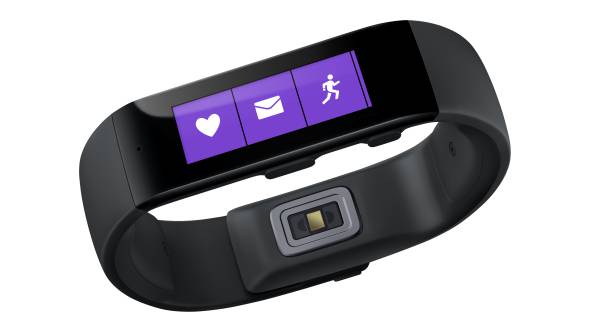
To briefly recap the non-Band items from our Wearables 2014 article, Microsoft Health is a cloud service, such as OneDrive, that aims to help improve the health of its users through data analysis and actionable feedback ("insights"). Activity tracking devices and apps that connect to Microsoft Health publish data, with your permission, to the Microsoft Health server. Microsoft claims their cloud data framework and analysis provides the only total health service available. Additionally, Microsoft Health is referred to as an open platform, therefore other companies can interface with it as both publishers of data and subscribers of analysis. Microsoft Health also connects to another Microsoft service, HealthVault, which contains personal and family medical information and lab results.
Previously, users of Microsoft Health could only access their data and insights through a corresponding smartphone application. That changes this week with the launch of https://dashboard.microsofthealth.com (which is either ironically down or simply unavailable to those without a Microsoft Band). This is a welcome addition as smartphones, with their limited screen sizes, simply cannot match the information density of a well designed website. Microsoft was clear to state the dashboard will also work well from a mobile browser should you choose not to use the app- for example if you're quickly using a friend's phone.
Additionally, Microsoft Health has now officially rolled out the previously announced support to connect with MapMyFitness and Microsoft HealthVault. Users can visit the "Connected Apps" section of their dashboard to enable the integration.
The rest of the updates announced this week are for the Microsoft Band, and there are quite a few:
- Bike Tile: The Bike Tile on users’ Microsoft Band lets them track their rides both indoors and outdoors, on the road or trail. Features include:
- Heart Rate Monitor: When the Bike tile is active, the heart rate monitor is optimized specifically for biking activities.
- Elevation Tracking: Track elevation and elevation gain, distance and duration and calorie burn– viewable in the Microsoft Health app.
- GPS: Users can activate GPS on their Band to map their ride in the mobile app and share it with their friends via email.
- Speed Analysis: Track your current and average speeds both on the band and in the mobile app, and review your custom splits to relive those longer bike rides.
- Recovery: From the mobile app, users can see an estimate for how long it will take their body to recover from the ride.
- Web Dashboard: Biking functionality is supported by the Microsoft Health mobile app at launch. Integration with the Microsoft Health web dashboard is coming soon.
- Guided Workouts: Five new indoor biking workouts have been added to the Guided Workouts portfolio, including: Indoor Bike Tabata Sprints, Indoor Bike Hour of Sweat, Indoor Bike Total Body, Indoor Bike Pyramid, and Indoor Bike Intervals.
- Quick Read: Quick Read provides another option to scan incoming texts, emails and other notifications. When enabled, notifications are displayed in a large font size and in rapid succession of words enabling users to read messages while in motion and without the need to scroll.
- Virtual Keyboard & Voice Replies for Windows Phone 8.1 Users: Windows Phone 8.1 users can craft replies to text messages in two ways. Users can reply to text messages using the virtual keyboard with minimal errors with the help of Microsoft’s World Flow technology, which predicts commonly used words and phrases. They can also dictate responses with voice, powered by Cortana.
Generally, the band is now suitable for biking, and Quick Read and Virtual Keyboard are added to bolster the smart watch use case. From my own experience wearing a Moto360, the Quick Read and Virtual Keyboard functionality are interesting. Receiving a text message appropriately vibrates my wrist with the Moto360, but I need to tap and slide the display around to read the contents. It appears Quick Read can save that extra step.
The Virtual Keyboard honestly sounded impossible to pull off on such a small display, and since I lack a review unit I can not try it. Windows Central has a write up and video of the functionality and it is truely impressive.
The keyboard is an option when replying to text messages and it uses the same excellent swiping technology present in Windows Phone 8.1, Word Flow. Anand has written about Word Flow before. This is an welcome addition, as using voice recognition simply is not perfect yet. I have sent too many voice dictated replies to my wife that state "at the Jim" or something even less recognizable.

Finally, Microsoft has unveiled the Microsoft Band SDK Developer Preview, enabling iOS, Android, and Windows Phone apps to access the Band's sensors and create tiles linked to the application on the Band itself.
Thankfully, as every wearable (save the Samsung Gear S) lack cellular connectivity, there is typically no lengthy mobile operator validation delay. The Microsoft Band update is rolling out starting yesterday and should arrive at all owners within a few days.
More...
- Bike Tile: The Bike Tile on users’ Microsoft Band lets them track their rides both indoors and outdoors, on the road or trail. Features include:
-
02-24-15, 01:30 PM #4766
Anandtech: Pebble Announces the Pebble Time
The original Pebble watch was arguably the first device in what is now a rapidly growing smartwatch segment of the wearables market. Since its release, the software of the Pebble has steadily improved, and Pebble has introduced various new color options as well as more premium version of the Pebble called the Pebble Steel. But even with all those changes, the fundemental hardware of the Pebble remained the same. Today Pebble has announced a brand new smartwatch called the Pebble Time, and it is what one could call a true successor to the original Pebble.
The Pebble Time retains many of the software features that users enjoy from the original Pebble. It's compatible with every existing Pebble application and watchface, and it has the same battery life of up to seven days. But the hardware of the Pebble Time is significantly improved from the original Pebble. The area that most users will notice first is the new display. While the original Pebble used a black and white memory LCD, the Pebble Time uses a color e-paper display. The design and size of the watch is also improved, with the thickness of the case having been reduced to 9.5mm, which is 20% thinner the original Pebble. The bottom of the case is also curved to fit more comfortably on the user's wrist.
On the software side of things, the Pebble Time uses a new interface that Pebble are calling Timeline. Essentially, the interface is a sequential list of the events that you have planned throughout the day, and the three buttons on the right side of the watch allow you to move to the past, present, or future of your daily timeline. Like the original Pebble, the Pebble Time works with both Android and iOS devices, but features like sending voice replies to incoming notifications are more limited on iOS.
The Pebble Time will intiially come in black, white, and red. For their initial sales run Pebble has gone back to Kickstarter, the website where they originally began. The Pebble Time will retail for $199 when the Kickstarter campaign is over, but users who want to purchase one now can get it for $179 on Pebble's Kickstarter campaign below.
Source: Pebble Time Kickstarter
More...
-
02-24-15, 02:01 PM #4767
Anandtech: Embedded World 2015: Skylake-DT Industrial Motherboard Spotted
Even with Broadwell not completely out of the door, a lot of attention is being put towards Skylake, the 14nm architecture update from Intel. Current information out the wild seems to contain a lot of hearsay and supposed leaks, but now we actually have at least some indication that Skylake is coming thanks to ComputerBase.de who spotted an ASRock industrial motherboard with the LGA1151 socket for Skylake processors at Embedded World.
Given how far Skylake is away from market, chances are that this motherboard is a mock-up rather than a working unit as we would imagine Intel to still be working on the first round or two of CPU steppings at this point. The motherboard does show up some interesting differences to Haswell, such as the socket which moves the notches higher up to the corners:
One of the big talking points of Skylake is the DDR4 compatibility, but this board throws a spanner into that by supporting two DDR3L-1600 SO-DIMM slots for up to 16GB of memory. It is also worth noting the separate chipset (most likely a server grade C236 for the next Xeon E3 CPUs) and support for three HDMI ports on the board.
ComputerBase.de also photographed a roadmap showing the boards on offer along with chipsets and some specifications:
Here we see C236 for workstations, Q170/H110 for Desktop (presumably mirroring Q and H chipsets like we have now), QM170 for mobile and at the end is the Atom SoCs. The specifications show desktop CPUs at 35, 65 and 95W, with the 95W being slightly up from Haswell. Mobile CPUs fall in at 15-45W, while the Atom details are thin on the ground. All the boards with memory listed have DDR3L as the main memory type, and in most cases the boards have Q3/Q4 2015 sampling availability with Q1 2016 as the mass production date.
Can we take much information away from this? Aside from TDP numbers and chipset naming, the remarking thing is the DDR3L support, especially with the expectation that Skylake will be DDR4. One thing is for certain is that the motherboard companies are definitely in a situation where designing and building boards for Skylake is on the agenda. It makes me wonder if Embedded World has any more similar motherboards to be seen, and how many we will see at Computex in June.
Source: ComputerBase.de
Gallery: Embedded World 2015: Skylake-DT Industrial Motherboard Spotted


More...
-
02-24-15, 07:00 PM #4768
Anandtech: ZyXEL Launches Affordable 10G Switches, Brings UTM Devices to Home Users
ZyXEL has a track record of making affordable networking equipment for both home users and service providers. Post-CES, the company has made a couple of product line announcements that warrant perusal from those keeping track ofdevelopments in the wired networking space.
Affordable 10G Switches
The first product line targets enterprise users thinking about shifting to 10G. With platform advancements bringing down the price and power consumption for 10GBASE-T switches, we have seen a host of affordable switches enter the market from various manufacturers. Netgear took the lead a couple of years back with a number of ProSafe 10GBASE-T switches starting at $1400 for the 8-port model. A couple of years down the road, the prices have come down considerably (slightly more than $800 for the 8-port model).
ZyXEL is now entering the affordable 10GBASE-T market with two switches, the Web Smart XS1920-12 and the L2 Managed XS3700-24. The two models are compared in the table below
ZyXEL is also touting their ZON management platform which enables IT administrators to have a unified view and streamlined control of various devices in the network. The new 10G switches are obviously compatible with the ZON platform.ZyXEL XS1920-12 vs. XS3700-24 Comparison Aspect XS1920-12 XS3700-24 Switch Class Smart Managed Layer 2 Plus (Layer 3 Lite) Port Distribution 10x 10GBASE-T
2x 10G (SFP/RJ-45)8x 10GBASE-T
12x 10G SFP+
4x10G (SFP/RJ-45)MSRP (USD) $1865 $3860 Switching Capacity (Gbps) 240 480 Forwarding Capacity (Mpps) 178.6 357.14 Packet Buffer (Byte) 2M 4M MAC Address Table 16K 16K IP Address Table - 512 Routing Entries - 64 Routing Domains - 128 Management IPv6 Management
Web GUIIPv6 Management
CLI
Web GUI
Out-of-bound Management PortStatic IP Routing - Yes VRRP - Yes Spanning Tree (STP/MSTP/RSTP) Yes Yes QoS Features 802.1p QoS
8 priority queues
Data prioritization (SPQ/WRR/WFQ)
v1 IGMP snooping
MVR
12K jumbo frames802.1p QoS
8 priority queues
Data prioritization (SPQ/WRR/WFQ)
v1, v2, v3 IGMP snooping
MVR
12K jumbo framesSecurity Features MAC freeze
802.1X authentication
TACACS+/RADIUS
L2/L3/L4 ACL security filterMAC freeze and intrusion lock
802.1X authentication
TACACS+/RADIUS
L2/L3/L4 ACL security filter
sFlowPower Supply and Features 100 - 240V AC, 50 / 60 Hz
Max. Power Consumption - 95.6 W100 - 240V AC, 50 / 60 Hz
Redundant Removable Power Supply Modules
Max. Power Consumption - 143.1 W (Single PSU), 161 W (Dual PSU)Physical Aspects 17.32 x 12.99 x 1.75 in.
9.27 lbs
326 BTU/hr Heat Dissipation17.32 x 17.24 x 1.73 in.
16.3 lbs
488 (single PSU) / 549 (dual PSU) BTU/hr Heat Dissipation
Removable fan module
UTM for Home Consumers
Towards the middle of last year, ZyXEL updated their UTM (Unified Threat Management) solutions for SMBs. In what we believe is a first from any home networking equipment vendor, ZyXEL is marketing the 4-port solution in the home consumer market too. Security is becoming an important aspect of home networks (with the rise in popularity of home automation devices and other online activities making home consumers vulnerable to cyberattacks) and ZyXEL is hoping to latch on to this opportunity with the USG40HE.
The USG40HE has a WAN port and 3 LAN/DMZ ports. There is an additional port that can be configured as a secondary WAN or another LAN port. Claimed firewall and VPN throughputs are 400 Mbps and 100 Mbps respectively.
This UTM device / home network security product provides firewall capabilities, content filtering, traffic prioritization depending on application recognition, intrusion detection and prevention and optional anti-virus / anti-spam capabilities. Similar to the tradition in the SMB market, ZyXEL is bundling a 1-yr license for the UTM services. Street price seems to be around $250, while the business edition is closer to $300. The latter comes with anti-virus and anti-spam licenses for 1 year, while the home edition makes them optional.
As home networks become more and more powerful, we believe the trend in the market (at least for power users) will be to move from an advanced Wi-Fi router to a gateway / wired router + Wi-Fi access point. The USG40-HE does fit into that scenario. That said, the 1-yr licensing for UTM capabilities works well in
business use-cases, but it might create a negative mindset for home consumers who are not used to such business models. It will be interesting to see how this product fares in the market.
More...
-
02-25-15, 02:30 PM #4769
Anandtech: Motorola Announces Moto E (2015): Cortex-A53 + LTE For $149
Today Motorola has announced the launch and immediate availability of the 2015 version of the Moto E, the latest member of the company’s line of low-end smartphones.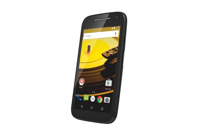
The 2015 edition of the Moto E is a pretty hefty upgrade of a phone launched just 9 months ago. In terms of design the new Moto E is generally a bigger, more powerful version of its predecessor, retaining the same rounded plastic design while enlarging the overall body slightly to house the larger 4.5’ screen. Meanwhile Motorola has iterated on the 2014’s swappable back covers, with the 2015 featuring the ability to swap in one of the company’s newer grip shells, or the phone’s colored bands can be swapped out separately.
[TR="class: tgrey"]
[TD="colspan: 7, align: center"]Motorola's 2015 Low-End Smartphone Lineup[/TD]
[/TR]
[TR="class: tlblue"]
[TD="width: 120"] [/TD]
[TD="width: 170"]Motorola Moto E (2015)[/TD]
[TD="width: 170"]Motorola Moto E (2014)[/TD]
[TD="width: 170"]Motorola Moto G (2014)[/TD]
[/TR]
[TR]
[TD="class: tlgrey"]SoC[/TD]
[TD="width: 170, align: center"]Qualcomm Snapdragon 410 (MSM8916)
4x Cortex A53 @ 1.2GHz
Adreno 306 at 400MHz
(LTE model XT1527)
or
Qualcomm Snapdragon 200 (MSM8x10)
4x Cortex A7 @ 1.2GHz
Adreno 302 at 400MHz
(3G models)[/TD]
[TD="width: 170, align: center"]Qualcomm Snapdragon 200 (MSM8x10)
2x Cortex A7 @ 1.2GHz
Adreno 302 at 400MHz[/TD]
[TD="width: 170, align: center"]Qualcomm Snapdragon 400
(MSM8x26)
4x Cortex A7 @ 1.2 GHz
Adreno 305 at 450MHz[/TD]
[/TR]
[TR]
[TD="class: tlgrey"]RAM/NAND[/TD]
[TD="width: 170, align: center"]1GB LPDDR3
8GB NAND
& MicroSD[/TD]
[TD="width: 170, align: center"]1GB LPDDR2
4GB NAND
& MicroSD[/TD]
[TD="width: 170, align: center"]1GB LPDDR3
8/16GB NAND[/TD]
[/TR]
[TR]
[TD="class: tlgrey"]Display[/TD]
[TD="width: 170, align: center"]4.5" 960x540 LCD[/TD]
[TD="width: 170, align: center"]4.3" 960x540 LCD[/TD]
[TD="width: 170, align: center"]5" 1280x720 IPS LCD[/TD]
[/TR]
[TR]
[TD="class: tlgrey"]Dimensions[/TD]
[TD="width: 170, align: center"]129.9 x 66.8 x 12.3mm
145g[/TD]
[TD="width: 170, align: center"]124.38 x 64.8 x 12.3mm
142g[/TD]
[TD="width: 170, align: center"]141.5 x 70.7 x 11.0 mm 149g[/TD]
[/TR]
[TD="class: tlgrey"]Camera[/TD]
5MP (2592
More...
-
02-25-15, 08:00 PM #4770
Anandtech: Samsung Announces 128GB UFS Storage For Smartphones
We've first heard about plans to adopt UFS (Universal Flash Storage) with the announcements of Toshiba and Qualcomm reported over a year ago. While the promised late 2014 schedule seems to have been missed, and we still haven't seen any major product with the technology, it looks like UFS is finally gaining some traction as today Samsung is announcing the mass production of in-house solutions based on the UFS 2.0 standard.
Samsung claims to provide the new embedded memory type in 32GB, 64GB and 128GB capacities. The 128GB model doubles the amount of storage even their biggest eMMC storage solution is able to deliver. It was only last week that Samsung recently released a new eMMC 5.1 based NAND line-up which promised major gains over today's deployed eMMC products.
The UFS solution claims to achieve 19K IOPS (Input/output operations per second) in reads, almost double that of the 11K IOPS their eMMC 5.1 solution is capable of, and 2.7X times what common embedded memory is capable of today. There is also a purported boost to sequential read and write performance to SSD levels, although Samsung doesn't provide any actual figure, so we'll have to wait until we review a device to see what the actual gains are. What should be very interesting is a promised 50% decrease in energy consumption. We're still not very sure on the impact of eMMC power on a smartphone's battery life, but scenarios such as video recording are certain use-cases where a decrease in NAND power could be very beneficial to battery life.
UFS is based on a serial interface as opposed to eMMC's parallel architecture, enabling Full-Duplex data transfer and achieving twice to four times the peak bandwidth (depending on implementation) over the existing eMMC 8-bit interface.
Samsung offers the solution also in an ePoP package, meaning the NAND IC is embedded with the RAM ICs in a PoP package on top of the SoC, a solution already employed in the Galaxy Alpha and Galaxy Note 4. The goal here is to save on precious PCB space in small form factors such as smartphones.
We're looking forward to see in what kind of devices Samsung implements the technology and how it affects their performance and responsiveness.
Source: Samsung Tomorrow
More...


 Quote
QuoteThread Information
Users Browsing this Thread
There are currently 18 users browsing this thread. (0 members and 18 guests)


Bookmarks