

Results 5,281 to 5,290 of 12094
Thread: Anandtech News
-
08-26-15, 08:31 AM #5281
Anandtech: The Intel Broadwell Xeon E3 v4 Review: 95W, 65W and 35W with eDRAM
Our Broadwell coverage on the desktop has included reviews of the two consumer processors and a breakdown of IPC gains from generation to generation. One issue surrounding Broadwell on consumer platforms was that the top quad-core model was rated at one third less power in comparison to previous Intel quad core processors. Specifically, Broadwell is 65W against 84-95W in past generations. This puts Broadwell’s out-of-the-box peak performance at a TDP (and frequency) disadvantage. However in a somewhat under-the-radar launch, Intel also released a series of Broadwell Xeons under the E3-12xx v4 line. We sourced three socketed models, the E3-1285 v4 at 95W, the E3-1285L v4 at 65W and the E3-1265L v4 at 35W to get a better scope of Broadwell's scaling across different power requirements.
More...
-
08-26-15, 11:32 AM #5282
Anandtech: Exploring Intels Omni-Path Network Fabric
For several months now we have been talking about Intel’s Omni-Path network fabric, the company’s next-generation 100Gbps netwoking fabric technology. Typically Omni-Path has come up alongside discussions of Intel’s forthcoming 2nd generation of Xeon Phi products, codenamed Knights Landing. With Intel designing the two products alongside each other, and with Knights Landing due later this year, the company is now opening up a bit more about Omni-Path and how it works, including a paper on the technology for the IEEE Hot Interconnects conference this week and a press briefing on the technology at last week’s Intel Developer Forum 2015.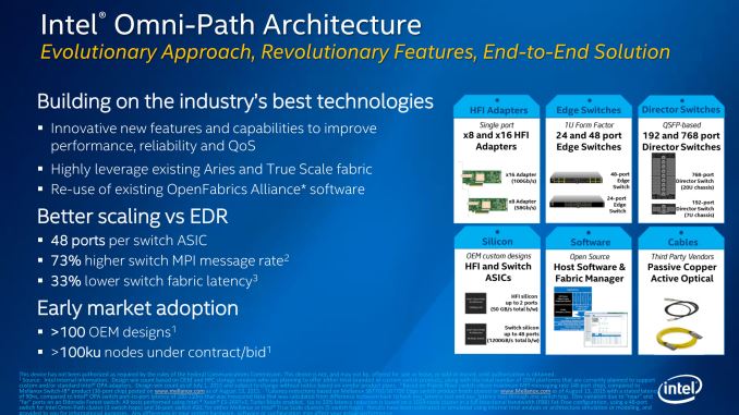
Intel is of course no stranger to network fabrics, having produced InfiniBand gear for a number of years under their True Scale brand. In 2012 the company went on a buying spree, picking up both QLogic’s InfiniBand technology and Cray’s interconnect technology as well. The long goal for Intel has been to develop a successor to InfiniBand and True Scale, one that would scale faster, better, and cheaper. The end result of these development efforts has been the creation of Omni-Path and the surrounding ecosystem.
For Intel developing Omni-Path solves several goals for the company, many of them unsurprisingly tied closely to Xeon Phi. On the whole, fabric costs as a percentage of total HPC system costs has been going up, which for Intel is a problem on multiple levels. It decreases the amount of the bill of materials spent on Xeon Phi and other Intel hardware, it drives up overall system costs, and it presents a barrier to entry for customers. This has led to Intel to focus on bringing the cost down on fabrics, which in turn has led to the development of Omni-Path.
The current Q-Logic True Scale Controllers
The biggest focus for Intel as far as costs control go is to work on integration, as over time integration brings down the number of components required and therefore brings down costs as well while increasing reliability. For this reason we will see versions of Knights Landing co-processors launching with on-package Omni-Path capabilities, although not in a full integrated fashion. In this case the company will be installing Omni-Path controllers on to Knights Landing chip packages in an MCM manner, meaning that the Knights Landing silicon itself won’t feature Omni-Path but the chip will, both sharing the PCIe interface. This ultimately sets the stage for future generations of Omni-Path and Xeon Phi by getting vendors and customers used to having it on-chip, with the successive (second) generation finally going fully integrated. The applicability extends to data leaving the Xeon Phi through the fabric without requiring further intra-node data organization.
Meanwhile as not every host will be a Xeon Phi, Intel is also developing PCIe Omni-Path cards as well. The cards will depending on the specific model support one or two Omni-Path ports via either PCIe 3.0 x16 or x8, though you’ll need the x16 card for full 100Gb/sec bandwidth. The TDP on these cards is said to be 8W, with a max power draw of 12W.
Along with the host adapters, Intel will also be designing other hardware elements of Omni-Path, such as switches, which will scale up to 48 ports per switch. The fact that Intel will be offering a 48 port switch is something that they consider to be a feather in their cap for Omni-Path, as larger switches allow for flatter network topology. With similar InfiniBand switches only scaling up to 36 ports per switch, a 48 port switch represents a 33% increase in the number of ports that can be switched. For a theoretical “sweet spot” one-thousand node Omni-Path design then, this would allow every node to be no more than 3 hops from any other node, whereas a topology with 36 nodes would stretch that out to 5 hops. The benefit of fewer hops, besides being fewer switches, is that it reduces the maximum latency for the fabric since any given packet will traverse fewer switches to get to its destination.
OPA Host Controller Engineering Sample
Omni-Path Fabric ArchitectureDiving into the fabric architecture itself, for Omni-Path Intel has attempted to prudently develop the architecture in such a way that it will outperform similar technologies (e.g. InfiniBand EDR), but also to do so while controlling costs. A big part of this has been designing the fabric to withstand higher bit error rates, as the greater error tolerances drive up the cost of the fabric, both with regards to equipment cost and the use of more expensive optical cable runs versus cheaper copper cable runs. To that end Intel is shooting for a bit error rate of 1E-12, or roughly a single bit error every 10 seconds when operating at 100Gb/sec.
Surprisingly, to manage these errors Omni-Path doesn’t use any form of error correction such as Forward Error Correction, but instead relies on a simpler CRC/retransmit mechanism. This is based on citing the fact that forward error correction causes a fair bit of latency due to the need to at two different packet levels, and then retransmit any failed packets from end-to-end. Omni-Path by comparison allows re-transmission at the hop-to-hop level, minimising latency and supporting a higher bit-error rate as a result. This means that Omni-Path does need to stop and request a retransmission end-to-end, but for a standard low-level packet error it can request the retransmission from the previous node as soon as it’s discovered, before a packet even moves through the switch to its target node.
Speaking of packets and links, for Omni-Path Intel has devised an interesting method of operating the fabric. Breaking a bit from the traditional 7 layer OSI model, the Omni-Path model essentially has two layers of packets, manifesting itself as an in-between layer of the model. The closest thing to traditional packets offered by Omni-Path is the Fabric Packet (FP), a node-to-node packet type that is generated by higher levels of the stack. However FPs aren’t transmitted as-is, and instead are broken down into what Intel calls the Link Transfer Packet (LTP). The LTP is a smaller link-local packet, and with Intel describing this as a kind of Layer 1.5 packet. It is at this level that retransmission of packets occurs in the event of bit-errors.
It’s at the LTP layer where most of the real work takes place. The LTPs are 1056 bits in length and contain a combination of data (1024 bits), FLIT type bits (16 bits, 1 for each FLIT), CRC information (14 bits), and what Intel calls virtual lane credit bits (2 bits). On the data side, the 1024 data bits are in turn split up into 16x 64-bit Flow Control Digits (FLITs), which are ultimately the smallest unit of data. As LTPs can contain FLITs from multiple FPs, the FLITs are how data from multiple FPs within a single LTP is kept organized.
Overall the fact that the LTP is 1056 bits in size and contains 1024 bits of data gives the LTP an efficiency equivalent to 64/66b encoding, similar to other fabric standards. Intel uses a bit-scrambler here in order to provide the necessary protection against running disparity without having to use further encoding and padding on top of the LTP. Coupled with this, Intel ever so slightly overclocks the Omni-Path link layer, such that it runs at 25.78125Gbps, which after the overhead of the LTP gives Omni-Path a proper 100Gb/sec of bandwidth at the link layer level.
Getting back to error resilience for a moment then, we can see how error detection and transmission works under this model. The LTPs having their own 14-bit CRC means that a link can request a retransmission should an LTP become corrupt, catching it after just 1056 bits and before an LTP moves on to the next link in a route. Meanwhile, in the unlikely event that an error still makes it through, then the FP error check at the destination node will find the error and trigger a retransmission of the whole FP.
Finally, let’s talk a bit about packet prioritization, via what Intel calls Traffic Flow Optimization. Because LTPs can be composed of data from multiple FPs via the use of FLITs, Omni-Path has a relatively simple method to handle packet prioritization. Higher priority FPs are simply given space on the current LTP, bumping the lower priority FP already in progress, and the lower priority FP can complete whenever it is not being blocked by higher priority traffic. Intel cites this as giving Omni-Path better latency, as higher priority packets have a minimal wait time (a 16-bit FLIT) before being able to assume control of the link. Overall Omni-Path supports 32 priority levels, though Intel expects first-gen setups to use something between 4 and 8.
Closing ThoughtsWhile the purpose of Intel’s Omni-Path disclosure is in part to help advertise the technology and entice potential customers looking for a 100Gb/sec fabric, Intel does already have some customers lined up for the fabric. The company is telling the press and public that there are already over 100 OEM designs in the pipeline, with bids/contracts on over 100K nodes in total.
Finally, given Omni-Path’s close development alongside Xeon Phi, unsurprisingly the two will be close together in deployment. As disclosed in Intel’s presentation, the company is already sampling OEMs. The first customer deployments are expected in Q4 of this year, with broader availability and rollout to follow in 2016.
More...
-
08-26-15, 01:30 PM #5283
Anandtech: Intel's Skylake GPU - Analyzing the Media Capabilities
At IDF in San Francisco last week, Intel provided us with lots of insights into Skylake, the microarchitecture behind the 6th generation Core series processors. Skylake marks the introduction of the Gen9 Intel HD Graphics technology. In advance of our full Skylake architecture analysis (coming soon), I wanted to get a head start and explain the media side (including Quick Sync and the image processing pipeline) of Skylake in a separate piece.
Media Capabilities and Quick Sync in Intel HD Graphics - A Brief History
Quick Sync has evolved through the last five years, starting with limited hardware acceleration and usage of the programmable EU array in Sandy Bridge. The second generation engine in Ivy Bridge moved to a hybrid hardware / software solution with rate control, motion estimation and intra estimation as well as mode decision happening in the programmable EU array. Usage of the EU array enabled tuning of the algorithms. Motion compensation, intra prediction, forward quantization and entropy coding were done in hardware in the MFX (multi-format codec engine). Haswell added JPEG / MJPEG decode to the MFX, a dedicated VQE (video quality engine) for low power video processing and a faster media sampler.
Around the time Broadwell was introduced, we had the major transitions taking place in the video codec front - HEVC adoption was picking up, and VP8 / VP9 was also gaining support. In order to tackle these aspects and build on consumer feedback, Intel made major updates to the media block / Quick Sync engine late last year.
Broadwell was also the first microarchitecture to support two BSDs (bit stream decoder) in the GT3 variants. Each BSD allows a set of commands to decode one video stream.


Broadwell's updates (when compared to Haswell) are summarized in the slide below.
The detailed discussion of Broadwell's media capabilities above is relevant to the improvements made in Skylake.
Skylake's Gen9 Graphics
The Gen9 graphics engine comes in multiple sizes for different power budgets. There are three main variants, GT2, GT3/GT3e and GT4e. In the slide below, the important aspect to note is that the media processing hardware (Media FF - Media Fixed Function) resides in the 'Unslice'. While the GT2 comes with the minimum possible Media FF logic, the GT3 and GT3e come with additional hardware capabilities. This strategy is similar to what was adopted in Broadwell.
The Unslice can operate at a different voltage and frequency compared to the Slices. This is especially important for video decoding / processing where the Media FF can run at higher clocks for better performance while ensuring minimal power consumption. From the viewpoint of tools such as GPU-Z and HWiNFO, it will be interesting to see if real-time statistics on voltage and clocks can be gathered for both the Unslice and the Slices. For additional power saving, power gating can be used at the Slices level or the EU group level.
Amongst the media improvements made in Skylake, we have:
- An additional fixed function video encoder in the Quick Sync engine
- Additional codec support (both decode and encode): HEVC, VP8, MJPEG
- RAW imaging capabilities
Quick Sync in Skylake
Intel classifies the Quick Sync modes in Broadwell and previous generations as 'PG-Mode' (Processor Graphics). It is optimized for faster than real-time encoding and flexibility. The new mode, 'FF-Mode' (Fixed Function) is optimized for real-time H.264 encoding, with focus on lowering the latency and reducing the power consumption. Except for programmable rate control, all other aspects of the encoding algorithm are handled in the MFX itself. Since rate control is in the hands of the application software, it is possible to do a 2-pass adaptive mode even with the FF hardware.
The new mode could possibly enable better user-experience with features such as Wi-Di, screen recording etc.. Note that Skylake offers developers the flexibility to use either the PG mode or the FF mode in their applications. PG mode still retains the TUx (Target Usage level) discussed in one of the above slides.
Skylake's MFX engine adds HEVC Main profile decode support (4Kp60 at up to 240 Mbps). Main10 decoding can be done with GPU acceleration. The Quick Sync PG Mode supports HEVC encoding (again, Main profile only, with support for up to 4Kp60 streams).
The DXVA Checker screenshot (taken on a i7-6700K, a part with Intel HD Graphics 530 / GT2) for Skylake with driver version 10.18.15.4248 is produced below. HEVC_VLD_Main10 has a DXVA profile, but it is done partially in the GPU (as specified in the slide above). VP8 DXVA profile doesn't seem to be activated yet. There are new DXVA profiles (enabled) for the SVC (scalable video coding) extension to H.264.
Video Post Processing & Miscellaneous Aspects
Additional improvements include a scalar and format converter (SFC) that can work with MFX and VQE (without using the EUs or the media sampler). This enables power-efficient rotation and color space conversion during media playback.
Yet another power-saving trick introduced in Skylake is the media memory bandwidth compression. The compression is lossless and managed at the driver level.
Skylake's VQE also brings about new features with RAW image processing support (16-bit image pipeline), spatial denoising and local adaptive contrast enhancement (LACE). Power efficiency is also improved, with claims of the VQE consuming less than 50mW during operation.
The new fixed function hardware in the performance-sensitive stages enables even low power mobile Skylake parts to support 4Kp60 RAW video processing. LACE support is not available for 4K resolution on the Y-series Skylake parts, though.
Display Capabilities
In terms of display support, Skylake can drive up to three simultaneous displays. The supported resolutions are provided in the table below. At IDF, Intel was showing off the Skylake platform driving three 4K monitors simultaneously.
One of the disappointing aspects is the absence of a native HDMI 2.0 port with HDCP 2.2 support. Intel's solution is to add a LSPCon (Level Shifter - Protocol Converter) in the DP 1.2 path. Various solutions such as the MegaChips MCDP28 family of products exist for this purpose. According to one of leaked Intel slides from earlier this year, the Alpine Ridge Thunderbolt 3 controller can also act as a LSPCon and provide a HDMI 2.0 output. At IDF, Intel indicated that we could see Alpine Ridge supporting HDMI 2.0 towards the end of the year (something corroborated unofficially by a few motherboard manufacturers)

The display sub-system also provides hardware support for Multi-plane Overlay (MPO) that allows alpha blending of multiple layers. This saves power by selective disabling of un-needed planes. Usage applications include certain video playback scenarios and HUD (heads-up display) gaming. The table below lists out the updated support for MPO as one moves from Broadwell to Skylake. The NV12 feature is particularly interesting from a media playback perspective - it is a video format that avoids conversion as video data moves between the decoder, post processing and the display blocks. With Skylake, post-decoded NV12 content can also be provided directly to a MPO display plane, and there is no need for the video post processor to do a NV12 to RGB conversion.
Intel indicated that the new Skylake MPO feature could save as much as 1.1W when playing back 1080p24 video on a 1440p panel - which is a substantial amount when mobile devices are considered. Power savings are also achieved by altering the core display clock based on the display configuration, number of displays and the resolution of each display.
Systems utilizing eDP with Windows 8.1 or later can also take advantage of hardware support for reducing refresh rate based on video content frame rate (for example, 24 fps video streams can be played after reducing the panel refresh rate to 48 Hz - eliminating 3:2 pull-down issues while also providing power savings). Obviously, the panel and TCON should support this.
Additional power saving can also be achieved on supported panels using Panel Self Refresh Media Buffer Optimization (PSR MBO). It is an Intel-developed optimization on top of the Panel Self Refresh feature of eDP 1.3.
Concluding Remarks
The media-related changes in Skylake's Gen9 GPU are best summarized by the slide below.
Skylake brings a lot of benefits to content creators - particularly in terms of improvements to Quick Sync and additional image processing options (including real-time 4Kp60 RAW import). However, it is a mixed bag for HTPC users. While the additional video post processing options (such as LACE for adaptive contrast enhancement) can improve quality of video playback, and the increase in graphics prowess can possibly translate to better madVR capabilities, two glaring aspects prove to be dampeners. The first one is the absence of full hardware acceleration for HEVC Main10 decode. Netflix has opted to go with HEVC Main10 for its 4K streams. When Netflix finally enables 4K streaming on PCs, Skylake, unfortunately is not going to be the power efficient platform that it could have been. The second is the absence of a native HDMI 2.0 / HDCP 2.2 video output. Even though a LSPCon solution is suggested by Intel, it undoubtedly increases the system cost. Sinks supporting this standard have become quite affordable. For less than $600, one can get a 4K Hisense TV with HDMI 2.0 / HDCP 2.2 capability. Unfortunately, Skylake is not going to deliver the most cost-effective platform to utilize the full capabilities of such a display.
More...
-
08-27-15, 01:02 AM #5284
Anandtech: Obi Worldphone Launches The Worldphone SF1 and SJ1.5
Today Obi Worldphone, the smartphone company co-founded by former CEO of Apple and former president of Pepsi John Sculley, launched two new smartphones targeted at emerging markets. The first of the new phones has two SKUs, which allows the devices to target three different price points in the low-end and mid-range sections of the smartphone market. You can check out the specifications of both new smartphones in the chart below.
As you can see, the Worldphone SJ1.5 targets the low end of the smartphone market, while the SF1 is a mid-range device. I personally think the SJ1.5 might have trouble competing with Motorola's Moto E in regions where there is LTE coverage, but it does offer a larger, higher resolution display, as well as a very large battery and dual-SIM slot support which is very important for customers in emerging markets. Unsurprisingly, the SJ1.5 has a polycarbonate chassis, although the specifications for it indicate that it uses a magnesium-titanium alloy inside for support.Worldphone SF1 Worldphone SJ1.5 SoC Qualcomm Snapdragon 615
1.5GHz 4x Cortex A53
1.11GHz 4x Cortex A53MediaTek MT6580
1.3GHz 4x Cortex A7RAM 2/3GB LPDDR3 1GB NAND 16/32GB NAND + microSD 16GB NAND + microSD Display 5” 1080p IPS 5” 720p IPS Network 2G / 3G / 4G LTE (MDM9x25 Cat4) 2G / 3G HSPA Dimensions 146 x 74 x 8mm, 147g 146 x 73 x 7.95mm, 131g Camera 13MP Rear Facing (IMX214) F/2.0, 1.12 micron 1/3.06" sensor 8MP Rear Facing (OV8865) F/2.2, 1.4 micron 1/3.2" sensor 5MP Front Facing 5MP Front Facing Battery 3000 mAh (11.4 Wh) 3000 mAh (11.4 Wh) OS Android 5.0.2 Android 5.1 Connectivity 5 GHz 2x2 802.11a/b/g/n +
BT 4.0,
USB2.0, GPS/GNSS2.4 GHz 802.11b/g/n +
BT 4.0,
USB2.0, GPS/GNSSSIM Dual SIM (Micro + Nano) Dual MicroSIM Launch Price $199 (2GB/16GB)
$249 (3GB/32GB)$129
In my opinion, the more interesting of these two devices is the Worldphone SF1. The SF1's chassis is made of reinforced fiberglass, and despite its 11.4Wh battery is only 8mm thick. In many ways, it reminds me of the OnePlus One in how it offers some high quality specifications at a low price. For $199 you get 2GB of RAM, 16GB of NAND, a 1080p display, Sony's IMX214 camera sensor, and Qualcomm's Snapdragon 615 SoC. Moving up to $249 gets you an additional gigabyte of RAM, and doubles your storage to 32GB. At least on paper, the Worldphone SF1 appears to give you more for your money than a phone like the Moto G, and it could have a significant impact when it launches in the EMIEA region in the near future.
The design of both the SF1 and the SJ1.5 reminds me a lot of the older Nokia Lumia smartphones like the Lumia 800, although there are a number of differences that give them a distinct appearance. I'm actually interested in trying one of these new devices to see how they feel in the hand and whether they live up to the expectations created by their specifications on paper. Obi Worldphone's listed specifications do have some oddities, such as the Worldphone SF1 launching with Android 5.0.2 while the SJ1.5 launches with Android 5.1. It's not clear if there are some errors or if the devices really will ship with two different versions of Android at launch.
Both the Worldphone SF1 and Worldphone SJ1.5 will be launching in the near future at both online and physical retailers in countries including but not limited to Vietnam, India, Tukey, Pakistan, South Africa, Nigeria, Thailand, and the United Arab Emirates. The Worldphone SF1 is priced at $199 and $249 USD depending on the model you purchase, while the Worldphone SJ1.5 will be $129.
Obi Worldphone via Engadget
More...
-
08-27-15, 04:02 AM #5285
Anandtech: Logitech Announces Artemis Spectrum G633 & G933 Audio Headsets
This morning Logitech is announcing an update to the company’s popular high-end gaming headsets, the G930 and G35. The new headsets are the Artemis Spectrum G633 and G933, and like their predecessors, share a common audio platform with wired and wireless connectivity respectively.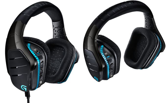
Logitech first introduced the G930 just over 5 years ago, and after many millions of units in sales they are finally updating these high-end headsets with the release of the Artemis Spectrum line. The Artemis headsets are a direct successor to the previous G series headsets, and while retaining the same high-end audio ambitions and 7.1 gaming features of their predecessors, they are also an almost entirely ground-up redesign of the headsets, both in physical form factor and underlying technology.Logitech Artemis Spectrum G633 G933 Frequency Response 20Hz - 20KHz Driver Size 40mm Pro-G Impedence 39 Ohms Microphone Size 4mm RGB Lighting Yes, 16.8M Colors 7.1 Surround Modes Dolby Headphone 7.1, DTS Headphone X Type Wired Wireless Inputs USB + 3.5mm Wireless + USB + 3.5mm Weight 374g 374g Launch Date September October MSRP $149.99 $199.99
Compared to the current G930/G35 headsets, the new Artemis platform retains the same 20Hz-20KHz frequency range, however Logitech has developed a new audio driver for Artemis which they are calling Pro-G. As a result of the new driver the impedance of the headsets have gone up slightly – from 32 Ohms to 39 Ohms – but so has the sensitivity, to 107dB SPL/mW. Logitech tells us that the new driver design is based on more thorough driver research over the past half-decade, and while headphone drivers are admittedly not a fast moving field, the Pro-G driver should deliver cleaner audio than the previous drivers.
Meanwhile Logitech has also been working on the boom microphone, shrinking it significantly from the G930. The microphone element in the Artemis platform is just 4mm in size, down from 6mm in the G930, allowing the overall boom mic size to be reduced.
Much more significant however has been the design of the headset itself, which sees a number of changes relative to the G930. Along with a new headband, Logitech has relocated the G-keys that were previously on the side of the left cup to the back edge of the left cup. Doing so has allowed Logitech to free up the sides of the cups for removable/replaceable covers, and more importantly for the wireless G933 model, similar to some of their mice Logitech can now store the USB dongle within the headset.
Top: Artemis Spectrum 4mm Mic. Bottom: G930 6mm Mic
The redesigned body also facilities the introduction of one of the headsets’ new marquee features, RGB lighting. Both Artemis headsets feature RGB LEDs in each cup, which in turn allow the back edge of the headset and the cover plates to be lit up. This admittedly seems to be one of the more gimmicky features of the new headset, serving no real acoustic purpose, but from a design standpoint there’s little arguing that LED gear continues to sell well.
The electronics within the headsets have also been updated. Using a new audio codec from Avnera, the Artemis platform now features the ability to mux audio from multiple sources. For the wired headset this means muxing the USB and 3.5mm inputs, and for the wireless headset this means muxing the USB and a 3.5mm input on the USB dongle itself, along with the 3.5mm input on the headset as well. Logitech calls this feature sound mixing, with the idea being that users can listen to multiple sources at once, e.g. a computer and TV, computer and phone, etc.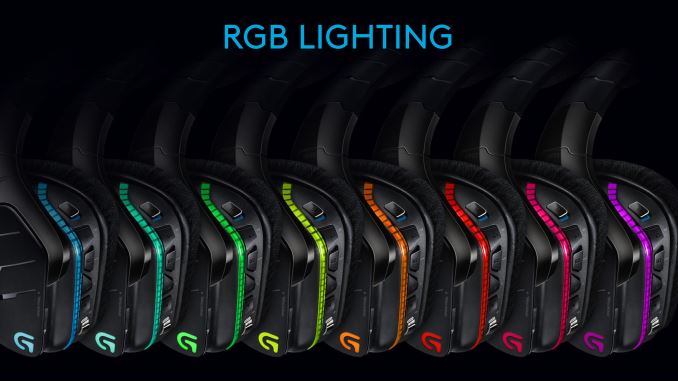
Speaking of which, like its predecessor the Artemis headsets feature a range of input options to work with PCs, consoles, and other consumer electronics. Both headsets feature a standard 3.5mm input/output for connecting to computers and consoles, and meanwhile the USB input works with a number of devices. Talking to Logitech, we’re told that the USB input presents itself as a 2 channel + mic solution, allowing it to be used with almost any USB device that supports USB headsets (e.g. console) and even Linux or OS X for that matter. However to make use of the Logitech’s 7.1 surround sound spatialization features, Windows and the appropriate Logitech gaming software are required.
For the Artemis platform Logitech is updating their gaming software as well to offer more 7.1 surround sound functionality, and this brings us to the Artemis headsets’ other marquee feature: DTS Headphone X. Along with their previous support for Dolby Headphone 7.1 surround sound spatialization, the Artemis headsets will also get DTS’s Headphone X technology as an alternative spatialization option. Similar to the Dolby option, DTS Headphone X is a 7.1 channel spatialization solution, but unlike Dolby Headphone DTS is said to be optimized for gaming as opposed to Dolby’s cinematic feel. Subjective improvements aside, DTS Headphone X does allow for some soundstage configuration, something Dolby lacks, which Logitech tells us should deliver more accurate (or at least desirable) spatialization performance for gaming. The one catch to DTS Headphone X is that it is not in the shipping version of the Logitech gaming software, and will not be available until October of this year.
Finally, for the G933 wireless version in particular, Logitech tells us that range and battery life are both improved over the G930. The headset now offers 15m range and battery life is up to 12 hours, versus 12m and 10 hours respectively. Furthermore thanks to the aforementioned use of the removable cup covers, it’s now possible to change the battery on the G933 without using any tools, simply by popping off the cover and swapping in the new battery. On a side note, after checking with Logitech we’re also told that the G933 still uses the 2.4GHz band for wireless connectivity, so despite the inherent interference in the 2.4GHz band, Logitech has been able to extend their range through a better wireless chipset and improved antenna characteristics.
Wrapping things up, while the Artemis Spectrum headsets are being announced today in time for this weekend’s PAX Prime event, the headsets themselves will not go on sale quite yet. The G633 wired headset will be available in September, and meanwhile the G933 wireless headset will go up in October. They will retail for $149 and $199 respectively.

More...
-
08-27-15, 07:33 AM #5286
Anandtech: AMD Announces Radeon R9 Nano; mini-ITX Card Shipping September 10th
Back in June at AMD’s R9 Fury X/Fiji GPU launch event, the company unveiled that there would be four products based on Fiji. Fury X and Fury – which have since launched – and then two additional products, the R9 Nano and a yet-to-be-named dual-GPU card. Uncharacteristicly for AMD, the R9 Nano was unveiled some time before it would ship in order to demonstrate some of the size benefits of the Fiji GPU and its HBM, with the card initially receiving a tentative launch date of “summer”.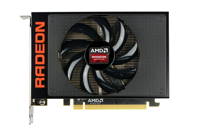
Now with August coming to a close, AMD is formally announcing the R9 Nano ahead of its full launch next month. The card, which will be AMD’s take on a premium, specialty product for the mini-ITX market, will be hitting retailer shelves on September 10th for $649.
Diving right into the design and specs, the R9 Nano is designed to be a showcase piece for the space savings that HBM technology offers. With Fiji’s 4GB of VRAM confined to a quartet of small, stacked packages near the GPU die, the overall space occupied by the complete GPU package is quite small, just over 1000mm2. Similar to what we saw with the R9 Fury X, the lack of large GDDR5 memory chips allows AMD to build a smaller board overall, and R9 Nano is to be the logical extension of what R9 Fury X started, bringing Fiji down to a mini-ITX sized video card.AMD GPU Specification Comparison AMD Radeon R9 Fury X AMD Radeon R9 Fury AMD Radeon R9 Nano AMD Radeon R9 390X Stream Processors 4096 3584 4096 2816 Texture Units 256 224 256 176 ROPs 64 64 64 64 Boost Clock 1050MHz 1000MHz 1000MHz 1050MHz Memory Clock 1Gbps HBM 1Gbps HBM 1Gbps HBM 6Gbps GDDR5 Memory Bus Width 4096-bit 4096-bit 4096-bit 512-bit VRAM 4GB 4GB 4GB 4GB FP64 1/16 1/16 1/16 1/8 TrueAudio Y Y Y Y Transistor Count 8.9B 8.9B 8.9B 6.2B Typical Board Power 275W 275W 175W 275W Manufacturing Process TSMC 28nm TSMC 28nm TSMC 28nm TSMC 28nm Architecture GCN 1.2 GCN 1.2 GCN 1.2 GCN 1.1 GPU Fiji Fiji Fiji Hawaii Launch Date 06/24/15 07/14/15 09/10/15 06/18/15 Launch Price $649 $549 $649 $429
In order to achieve this AMD has turned to a combination of chip binning and power reductions to make a Fiji card viable as the desired size. The Fiji GPUs going into the R9 Nano will be AMD’s best Fiji chips (from a power standpoint), which are fully enabled Fiji chips that have been binned specifically for their low power usage. Going hand in hand with that, AMD has designed the supporting power delivery circuitry for the R9 Nano for just 175W, allowing the company to further cut down on the amount of space required for the card.
The end result is that from a specification standpoint the R9 Nano should be an impressive, tiny terror. Since it’s a full Fiji GPU the R9 Nano doesn’t take an immediate hit to its performance relative to the R9 Fury X, featuring the same 4096 stream processors and 4096-bit ultra-wide HBM memory bus. The only real differences between R9 Fury X and R9 Nano are the clockspeed and the TDP/power targets. The R9 Nano will ship with a boost clock of 1000MHz versus R9 Fury X’s 1050MHz boost clock, and the TDP is 175W versus 275W.
The resulting performance difference in turn will come down to power limits. While R9 Nano has a 1000MHz boost clock, even with AMD’s binning 175W is a relatively harsh power limit for such a powerful GPU, and consequently the R9 Fury X the R9 Nano is expected to power throttle under normal circumstances. AMD tells us that the typical gaming clock will be around the 900MHz range, with the precise value depending on the power requirements of the workload being run. As to why AMD is shipping the card at 1000MHz even when they don’t expect it to be able to sustain the clockspeed under most games, AMD tells us that the higher boost clock essentially ensures that the R9 Nano is only ever power limited, and isn’t unnecessarily held back in light workloads where it could support higher clockspeeds.
Moving on, the physical board itself measures just 6” long, allowing the complete card to fit within the full width of a mini-ITX motherboard. Power delivery is handled by a single 8-pin PCIe power socket, which is becoming increasingly replacing the 2x 6-pin setup for 150W-225W cards. In order to get the length of the board down AMD has moved some of the power delivery circuitry to the back of the card; the front of the card still contains the inductors and heat-sensitive MOSFETs, while a number of capacitors are on the rear of the card (and is why you won’t find a backplate).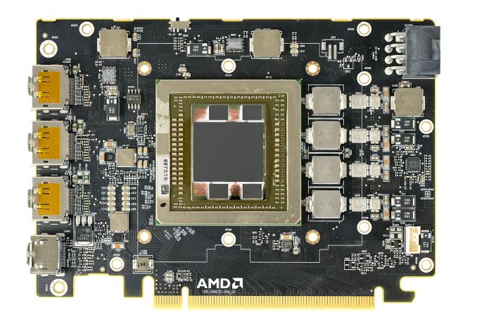
Responsibility for cooling the card falls to the R9 Nano’s new open air cooler, an aggressive design that has been specifically tailored to allow the card to effectively dissipate 175W of heat in such a small space. The overall design is best described as a combination open-air and half-blower hybrid; the design is technically open-air, however with only a single fan AMD has been able to align the heatsink fins horizontally and then place the fan in the center of the heatsink. The end result is that roughly half of the heat produced by the card is vented outside of the case, similar to a full blower, while the other half of the heat is vented back into the case. This reduces (though doesn’t eliminate) the amount of hot air being recycled by the card.
Drilling down, we find that the R9 Nano’s heatsink assembly is actually composed of two separate pieces. The primary heatsink is a combination vapor chamber and heatpipe design. A copper vapor chamber serves to draw heat away from the Fiji GPU and HBM stacks, and then heatpipes are used to better distribute heat to the rest of the heatsink. Meanwhile a small secondary heatsink with its own heatpipe is mounted towards the rear of the card and is solely responsible for cooling the MOSFETs.

The use of a vapor chamber in the R9 Nano makes a lot of sense given the fact that vapor chambers are traditionally the most efficient heatsink base type, however the R9 Nano is also unique in that we typically don’t see vapor chambers and heatpipes used together. Other designs such as the high-end GeForce series use a single large vapor chamber across the entire heatsink base, so among reference cards at least the R9 Nano stands alone in this respect, and it will be interesting to see what cooling performance is like.
That said, AMD is rather confident in their design and tells us that the R9 Nano should never thermally throttle; the card’s thermal throttle point is 85C, meanwhile the card is designed to operate at around 75C, 10C below the throttling point. Similarly, AMD is promising that R9 Nano will also be a quiet card, though as this is far more relative we’ll have to see how it does in testing.
From a marketing standpoint, AMD will be spending a fair bit of time comparing the R9 Nano to the reference R9 290X, AMD’s former flagship Hawaii card. The reference R9 290 cards were something of a low point for AMD in terms of cooling efficiency and noise, so they are eager to present the R9 Nano as an example of how they have learned from their earlier mistakes. Going up what is admittedly a low bar, AMD is telling us that the R9 Nano is 30% faster than the R9 290X, draws 30% less power than the R9 290X, and is much, much quieter than their former flagship. Thanks in large part to the combination of Fiji’s architectural improvements and AMD’s aggressive binning, the R9 Nano should offer around 2x the energy efficiency of the R9 290X, and of course it will be a much smaller card as well.
Otherwise against AMD’s Fury lineup, the performance of the R9 Nano will potentially be rather close. If AMD’s 900MHz average clockspeed figure proves to be correct, then the R9 Nano would deliver around 85% of the R9 Fury X’s performance, or around 92% of the R9 Fury’s. This would make it slower than either of the existing Fiji cards, but somewhere near (and likely ahead of) the R9 390X.
More importantly for AMD though, the R9 Nano should easily be the most powerful mini-ITX card on the market. The other major mini-ITX cards are based on smaller, less powerful video cards such as the Radeon R9 280 (Tonga) and GeForce GTX 970 (GM204), both of which a 900MHz Fiji will easily clear. By how much is going to depend on a few factors, including the actual average gaming clockspeeds and the games in question, but overall in the mini-ITX space there’s every reason to expect that R9 Nano will stand at the top.
Which brings us to the final aspect of the R9 Nano, which is pricing and positioning. For the R9 Nano AMD is going to positioning the card as a luxury product, similar to NVIDIA’s Titan series, which is to say that it will offer unparalleled performance for the segment of the market it’s designed for – in this case mini-ITX – but it will also fetch a higher price as a result. In the case of the R9 Nano, this means $650.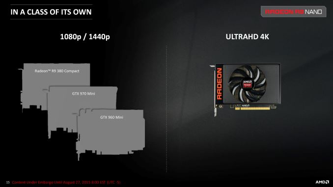
From a silicon lottery standpoint R9 Nano will feature AMD’s best Fiji chips, and the vapor chamber cooler, though not quite as intricate as R9 Fury X’s CLLC, is still an advanced cooler with a higher cost to go with it. As a result it’s unsurprising that AMD is seeking to charge a premium for the product, both to cover the higher costs and to take advantage of their expected performance lead within the mini-ITX market. Practically speaking the mini-ITX market is a small one relative to the larger gaming PC market (pun intended), and while there is some overlap with the power efficient gaming PC market, it’s hard to say just how much overlap there is. Regardless, AMD’s pricing and messaging make it clear that the R9 Fury series is intended to be AMD’s top performance cards and price/performance kingpins, while R9 Nano is a specialty card for a smaller market that’s currently underserved.
Of course there’s also going to be the question of how many cards AMD can even supply. Binning means that only a fraction of Fiji chips will ever make the cut, so R9 Nano is never going to be a high volume part along the lines of the R9 Fury series. What remains to be seen then is how much of a market exists for $650 mini-ITX cards, and then if AMD can supply enough cards for that market. Though given AMD’s unique situation, I don’t doubt that they’ll be able to sell a number of these cards.
On that note, we’re hearing that the overall Fiji supply situation is looking up. R9 Fury series cards have been in short supply in the US since the June/July launches, with card supplies improving just within the last couple of weeks. For the R9 Nano launch AMD has been stockpiling cards for the initial rush of sales, and beyond that we’ll have to see what becomes of the supply situation.
Finally, once the supply situation does improve AMD tells us that we may see some custom R9 Nano cards come later in Q4 of this year. AMD has been very vague on this point, but from what they’re telling us they’re going to be letting partners take a shot at developing Nano designs of their own. So while the launch on September 10th and for the next couple of months after that will be pure reference, we may see some custom designs by the end of the year.
And with that we end for now. Please be sure to check back in on September 10th for our full review of the smallest member of AMD's Fiji family.
Gallery: AMD Radeon R9 NanoSummer 2015 GPU Pricing Comparison AMD Price NVIDIA Radeon R9 Fury X
Radeon R9 Nano$649 GeForce GTX 980 Ti Radeon R9 Fury $549 $499 GeForce GTX 980 Radeon R9 390X $429 Radeon R9 390 $329 GeForce GTX 970 


More...
-
08-27-15, 08:30 AM #5287
Anandtech: The Cooler Master MasterCase 5 Review
Modular computer cases are not a new concept but attempts to produce actual retail products are very rare. Cooler Master is making a very bold move towards that direction with the MasterCase 5, their first design featuring the "Freeform" modular system. The company goes as far as to claim that their new case gives "absolute control over how the case looks and functions". That is a very bold statement and we will see to what extend that is true in this review.
More...
-
08-27-15, 11:37 PM #5288
Anandtech: Alienware Refreshes Lineup With Laptop Updates, And Liquid Cooled X51 Desk
Today Alienware announced some refreshes to its lineup. On the laptop front, the Alienware 13, 15, and 17 notebooks have been updated, and the Alienware 18 notebook has made a comeback. The X51 Desktop is also refreshed, and can now be used with the same Alienware Graphics Amplifier that was available for the notebooks.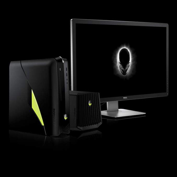
Starting with the laptops, the line was refreshed with the graphics amplifier as an option almost a year ago already, and the company says the new models have over 20 updates on tap. This includes USB Type-C ports for USB 3.1 and Thunderbolt 3 capabilities. Each of the laptops offers a different choice of processors, with the smallest of the bunch being outfitted with the 5th generation dual-core Core i5 and i7 U series, and the larger models offering quad-core 4th generation CPUs. On the GPU side, the NVIDIA GTX 960M graces the Alienware 13, the Alienware 15 offers a choice of the NVIDIA GTX 965M, GTX 970M, GTX 980M, or an AMD offering with the R9 M395X. The 17-inch model comes standard with the NVIDIA GTX 970M and can be upgraded to the GTX 980M. Unfortunately all models come standard with a spinning hard drive as the base option, but PCIe SSDs are available in all models. There are quite a few configurations available so it is easiest to reference this table. Alienware 15 with Graphics Amplifier
Alienware is also offering dynamic overclocking capabilities for the CPUs which will hopefully take some of the guesswork out of the task for the non-professional overclocker. On the networking side, Alienware has gone with the Killer Wireless-AC and Gigabit Ethernet combination similar to what we have seen from some of the competition.Alienware Laptops Alienware 13 Alienware 15 Alienware 17 CPU Intel Core i5-5200U (Dual-Core up to 2.7 GHz, 15w TDP)
Intel Core i7-5500U (Dual-Core up to 3.0 GHz, 15w TDP)Intel Core i5-4210H (Dual-Core up to 3.5 GHz, 47w TDP)
Intel Core i7-4720HQ (Quad-Core up to 3.6 GHz, 47w TDP)
Intel Core i7-4870HQ (Quad-Core up to 3.7 GHz, 47w TDP)Intel Core i7-4720HQ (Quad-Core up to 3.6 GHz, 47w TDP)
Intel Core i7-4870HQ (Quad-Core up to 3.7 GHz, 47w TDP)GPU NVIDIA GTX 960M 2GB NVIDIA GTX 965M 2GB
NVIDIA GTX 970M 3GB
NVIDIA GTX 980M 4GB
AMD Radeon R9 M395X 4GBNVIDIA GTX 970M 3GB
NVIDIA GTX 980M 4GBMemory 8-16 GB DDR3L-1600 (2 SODIMMs) Storage 500 GB 5400RPM Hybrid (8GB)
Optional 256 GB - 512 GB PCIe SSD plus 128 GB mSATA1 TB 7200RPM HDD
Optional 256 GB, 512 GB, 1 TB PCIe SSD boot drive plus 1 TB HDDDisplay 13.3" 1366x768 TN matte
Optional 1920x1080 IPS matte
Optional 3200x1800 IGZO IPS w/touch15.6" 1920x1080 IPS matte 17.3" 1920x1080 IPS matte
Optional 3840x2160 IGZO IPS mattePorts USB 3.0 x 2
USB Type-C 10 Gbps and Thunderbolt 3 x 1
HDMI 2.0
Alienware Graphics Amplifier Port
Media Card Reader (15 and 17 only)
HeadsetNetworking Killer 1535 802.11ac WiFi
Bluetooth 4.1
Killer e2400 Gigabit EthernetDimensions H: 1.04-1.098" (26.3-27.9 mm)
W: 12.91" (328 mm)
D: 9.25" (235 mm)H: 1.34" (34.0 mm)
W: 15.19" (385.8 mm)
D: 10.64" (270.2 mm)H: 1.35" (34.4 mm)
W: 16.93" (430 mm)
D: 11.49" (291.9 mm)Weight 4.54 lbs (2.06 kg) 7.07 lbs (3.21 kg) 8.33 lbs (3.78 kg) Battery 4 Cell 52 Whr, 130w A/C
Optional 4 Cell 62 Whr8 Cell 92 WHr, 180-240w A/C 8 Cell 92 WHr, 180-240w A/C Price $999+ $1199+ $1499+
The displays should be good, if the Dell XPS 13 is any indication. Similar to that device, the Alienware 13 will also offer a 3200x1800 IGZO display with touch. The 15-inch model has just one display option with a 1080p IPS matte panel, and the 17-inch model starts with a 1080p base offering but will also offer a UHD 3840x2160 IGZO IPS display. The large panel notebooks are one of the few mobile devices which would be capable of running UHD but to this point it has been difficult to get one over 1080p so this should be a nice treat. Alienware 17
All of these laptops can also be connected to the Alienware Graphics Amplifier which would give you access to a desktop class GPU if you need even more compute power.
Back after a hiatus is the Alienware 18 which we last saw back in 2013 when the dual GPU 18.4-inch monster was reviewed by Dustin Sklavos. There are different offerings, but it will offer dual GTX 970M with 12 GB of GDDR5, or dual GTX 980M graphics with a combined 16 GB of GDDR5 memory. The Intel CPU is going to be socketed, so customers will be able to upgrade it on their own, and it will ship with a factory overclock. The Alienware 18 will be available with up to 32 GB of system memory and four hard drives. The Alienware 18 Special Edition should be plenty capable, but once again the base model ships with a spinning disk, and you have to upgrade to a mSATA SSD boot drive which is a shame for a notebook which starts at $2500. Alienware 18
The extra-large laptop displays have not yet made the leap to high resolution, so the Alienware 18 is only available with 1080p offerings.Alienware Laptops Alienware 18 CPU Intel Core i7-4710MQ (Quad-Core, up to 3.5 GHz, 47w TDP)
Intel Core i7-4910MQ (Quad-Core, up to 3.9 GHz, 47w TDP)
Intel Core i7-4940MX Extreme Edition(Quad-Core, up to 4 GHz, 57w TDP, Overclocked up to 4.4 GHz)GPU NVIDIA GTX 970M 6GB x 2
NVIDIA GTX 980M 8GB x 2Memory 16-32 GB DDR3L-1600 (4 SODIMMs) Storage 1 TB 7200RPM HDD
Optional 512 GB mSATA SSD boot drive plus 1 TB HDDDisplay 18.4" 1920x1080 TrueLife Ports USB 3.0 x 4
Mini-DisplayPort
HDMI 1.4 Output / 1.3 Input
Media Card Reader
HeadsetNetworking 802.11ac WiFi
Bluetooth 4.0
Gigabit EthernetDimensions H: 2.23-2.26" (56.7-57.5 mm)
W: 17.97" (456.5 mm)
D: 12.91" (327.9 mm)Weight 12.06 lbs (5.47 kg) Battery 8 Cell 86 Whr Price $2499+
Finally, Alienware has refreshed its X51 desktop. The X51 fits in space wise between the small form factor Alpha and the large form factor Area-51. Alienware is targeting active keyboard and mouse gamers with this device, and the refreshed R3 model has moved to Skylake for the higher end models, and keeps a Haswell i3 model as the base. The $700 model comes with the NVIDIA GTX 745 GPU, and upgrades are available to the AMD Radeon R9 370 or NVIDIA GTX 960. There are a couple of interesting additions to this desktop. Alienware is offering a custom liquid cooling setup which should keep the temperatures in check, and will allow Alienware to offer overclocking of the CPU. It also adds support for the Alienware Graphics Amplifier which was first released on the notebook line. This may seem like an odd addition to a desktop, but the separate 460 watt power supply and chassis would allow a much larger GPU than could fit inside the small case of the X51. I think it is a neat addition especially if you have a laptop too, but it might be a hard sell to have someone buy a desktop and then buy something they have to put on the top of their desk.
Alienware Desktops Alienware X51 CPU Intel Core i5-6600K (Quad-Core Overlocked up to 3.9 GHz)
Intel Core i7-6700K(Quad-Core, Overclocked up to 4.4 GHz)Memory 8-16 GB DDR4-2133 GPU NVIDIA GTX 745M 4GB
NVIDIA GTX 750Ti 2GB
NVIDIA GTX 960M 2GB
AMD Radeon R9 M370 4GBStorage 1 TB 7200RPM HDD
2 TB 7200RPM HDD
Optional 256 GB SATA SSD boot drive plus 1 TB 5400RPM HDDFront Ports USB 3.0 x 2
Microphone
HeadphoneRear Ports USB 3.0 x 4
USB 2.0 x 2
HDMI 1.4
SPDIF
SpeakersNetworking DW 1506 802.11n
Optional Intel Single Band Wireless-AC 3165 w/Bluetooth 4.0
Gigabit EthernetDimensions H: 13.50" (343 mm)
W: 3.74" (95 mm)
D: 12.52" (318 mm)Weight Starts at 12.1 lbs (5.49 kg) Price $1100+ Alienware’s new products are all available now at Alienware.com.
Source: Dell
Gallery: Alienware Refreshes Lineup With Laptop Updates, And Liquid Cooled X51 Desktop


More...
-
08-28-15, 07:28 AM #5289
Anandtech: Blossom Smart Watering Controller Review
Home automation has garnered renewed attention, thanks to the Internet of Things (IoT) revolution. Many vendors targeting this market look to deliver solutions for aspects appealing to a broader audience. Some examples include lighting, temperature control, security using IP cameras etc. Irrigation control is a niche within the home automation niche. At first glance, it appears to be a limited market, as only those with gardens big enough to require scheduled / automated watering of multiple zones might need it. Surprisingly, there are many options for people looking to gain IP control over their irrigation / watering system's functioning. iConservo's Blossom is one such option. Read on for a detailed look at the Blossom Smart Watering Controller.
More...
-
08-28-15, 01:33 PM #5290
Anandtech: Valve and HTC Push Wide Release Of Vive VR Headset To 2016
Valve isn't a stranger to product delays or discrepancies between promised launches and when a product actually launches. This is often joking referred to as Valve Time, and it seems that Valve's hardware endeavors are no safer from it than their video games are. Today they announced that the wide consumer release of their Vive VR headset is being pushed to Q1 2016, a slight delay from the originally promised launch by the end of 2015.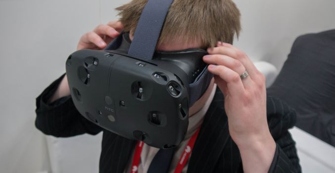
While the Vive will only begin to ship in volume in 2016, Valve and HTC will still be sending a limited number of units to developers and community members in the last quarter of this year. This means that they're technically fulfilling their promise to launch by the end of 2015, but not in the way most people were expecting.
With the Vive launching in Q1 2016, it's now in even deeper competition with the Oculus Rift and Project Morpheus from Sony which will also be launching during that quarter. The price for the Vive is still unknown, but with a small launch still occurring this year we won't have to wait much longer to find out.
More...


 Quote
Quote
Thread Information
Users Browsing this Thread
There are currently 10 users browsing this thread. (0 members and 10 guests)


Bookmarks