

Results 5,371 to 5,380 of 12096
Thread: Anandtech News
-
09-24-15, 08:39 AM #5371
Anandtech: Fable Legends Early Preview: DirectX 12 Benchmark Analysis
DirectX 12 is now out in the wild as a part of Windows 10 and the updated driver model WDDM 2.0 that comes with it. Unlike DX11, there are no major gaming titles at launch - we are now waiting for games to take advantage of DX12 and what difference it will make for the game playing experience. One of the main focal points of DX12 is draw calls, leveraging multiple processor cores to dispatch GPU workloads, rather than the previous model of a single core doing most of the work. DX12 brings about a lot of changes with the goal of increasing performance, offering an even more immersive experience, but it does shift some of the support requirements to the engine developers such as SLI or Crossfire. We tackled two synthetic tests earlier this year, Star Swarm and 3DMark, but due to timing and other industry events, we are waiting for a better time to test the Ashes of the Singularity benchmark as the game nears completion. Until that point, Microsoft's PR team got in contact with us regarding the upcoming Fable Legends title using the Unreal 4 engine, and a early access preview benchmark that came with it. Here are our results so far.
More...
-
09-25-15, 02:00 PM #5372
Anandtech: Netgear ReadyNAS RN202 2-bay NAS Review
NAS units with four bays present the best balance between cost and expandability for home consumers. However, with increasing hard drive sizes, two bays make the cut for many usage scenarios. The demand for high-performance, but cost-effective NAS units has been picking up, and this is where the modern ARM-based platforms come into play. Netgear's ReadyNAS 200 series was launched at CES and sported a Cortex A15-based Annapurna Labs SoC. Negear's offerings differentiates itself from the competition due to use of btrfs as the file system for the data volume. We have already looked at the Intel Atom-based RN312. In this review, we will take a look at how the ARM-based RN202 performs with the ReadyNAS OS, and see how the unit stacks up against the competitors in this space.
More...
-
09-28-15, 07:40 AM #5373
Anandtech: Zotac ZBOX MAGNUS EN970 Review - A Gaming mini-PC Done Right
In the course of our coverage of mini-PCs, we have seen offerings from vendors such as ASRock, GIGABYTE and Zotac targeting the gaming market. Usually, 'mini' doesn't fit the requirements of consumers in this space, but the appearance of power-efficient high performance GPUs have made the offerings in the gaming mini-PC space quite interesting. Zotac has been creating mini-PCs with a gaming focus by combining a mobile NVIDIA GPU with a Core U-series Intel CPU for a couple of generations now. Today, we have results from our evaluation of their Broadwell plus Maxwell combination, the Zotac ZBOX MAGNUS EN970.
More...
-
09-28-15, 07:40 AM #5374
Anandtech: iPhone 6s and iPhone 6s Plus Preliminary Results
At this point the iPhone release cycle is pretty well understood. One year, Apple releases the design refresh that changes the external design significantly while generally focusing on evolving the internal components. The year after, the S variant is released with the same design as the previous year, but with sweeping changes to the internals. This cycle of upgrades allows Apple to focus on updating one half of the iPhone at a time while essentially giving their teams a more comfortable two years to develop their next generation technologies.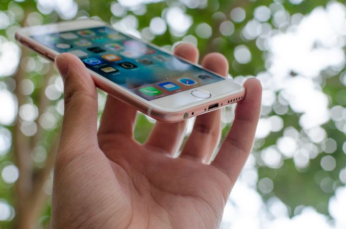
The iPhone 6s fits into this model quite well, with the introduction of new features like 3D Touch and a 12MP camera that supports 4K video recording. However, it’s often difficult to understand exactly how much has changed with an S model as Apple tends to focus on high level features, this despite the fact that so many of the changes in an S model are at a low level. While I haven’t had a lot of time with the iPhone 6s yet, I wanted to share some of the first results that I’ve acquired over the course of testing the iPhone 6s and 6s Plus in the past few days.
The first, and probably biggest change that I haven’t seen addressed anywhere else yet is the storage solution of the iPhone 6s. Previous writers on the site have often spoken of Apple’s custom NAND controllers for storage in the iPhone, but I didn’t really understand what this really meant. In the case of the iPhone 6s, it seems that this means Apple has effectively taken their Macbook SSD controller and adapted it for use in a smartphone. Doing some digging through system files reveals that the storage solution identifies itself as APPLE SSD AP0128K, while the Macbook we reviewed had an SSD that identified itself as AP0256H.
While the name alone isn’t all that interesting, what is interesting is how this SSD enumerated. One notable difference is that this storage solution uses PCI-E rather than SDIO, so it’s unlikely that this is eMMC. Given the power requirements, it’s likely that this isn’t the same PCI-E as what you’d see in a laptop or desktop, but PCI-E over a MIPI M-PHY physical layer. By comparison, UFS's physical layer is MIPI M-PHY as well, while the protocol is SCSI.
The iPhone 6s in turn appears to use NVMe, which rules out both UFS and traditional eMMC. To my knowledge, there’s no publicly available mobile storage solution that uses PCI-E and NVMe, so this controller seems to have more in common with the Macbook SSD controller than anything in the mobile space. It doesn’t seem this is an uncommon idea though, as SanDisk detailed the potential advantages of PCIE and NVMe in mobile storage at the Flash Memory Summit a month ago.
The controller is a critical part of any storage component, but without any NAND to control it’s a bit pointless. Fortunately, the NAND used appears to be exposed in the OS as it’s referred to as 1Y128G-TLC-2P. Breaking this down, the 1Y means that we’re looking at 1Ynm NAND process with TLC. The TLC portion might concern some, but as we’ll soon see it turns out that we’re looking at a hybrid SLC/TLC NAND solution similar to SanDisk’s iNAND 7232 eMMC and desktop SSDs like Samsung’s 850 EVO which is better suited to the bursty workloads seen in mobile and PC segments. Between the 128GB and 64GB units we currently have, the 64GB unit uses Hynix NAND, but it remains to be seen who is supplying the NAND for the 128GB variants and what other suppliers exist for the 64GB SKUs.NVMe eMMC Latency 2.8 µs N/A Maximum Queue Depth Up to 64K queues with
64K commands eachUp to 1 queue with
32 commands eachDuplex (Typical) Full Half
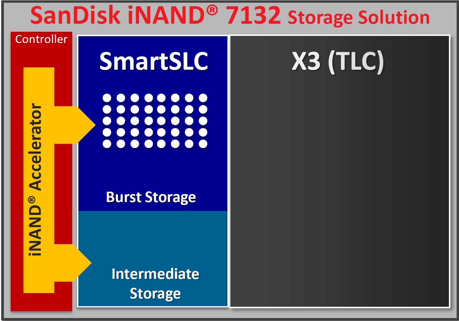 An example of how an SLC/TLC NAND storage device looks in mobile devicesFor those that are unfamiliar how these hybrid SLC/TLC NAND solutions work, in essence the SLC cache is made sufficiently large to avoid showing the reduced performance of TLC NAND. Any time you’re writing to the storage, the writes go to the SLC cache first before being committed to TLC NAND. As long as the overall average bandwidth demand doesn’t exceed the speed of the TLC, short-run bandwidth is solely limited by the speed of the SLC cache, which turns out to be the case for almost every normal use case.
In order to see how all of this translates into performance, we once again use StorageBench, which is an app that allows us to do 256K sequential and 4K random storage performance testing developed by Eric Patno and is comparable to AndroBench 3.6.
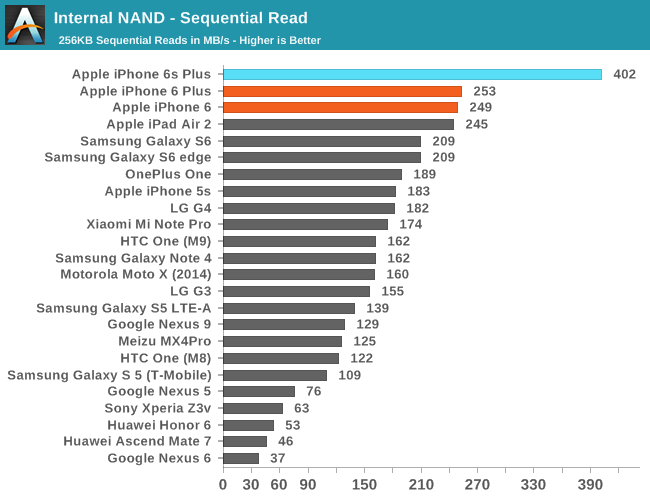
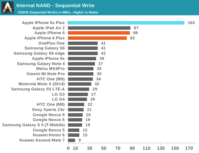
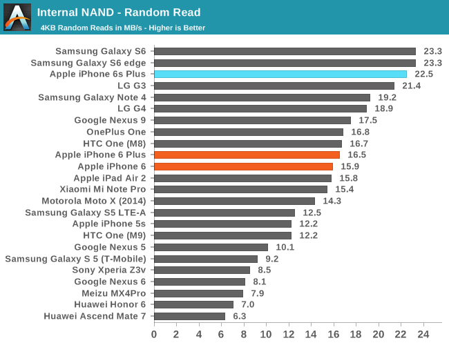 In practice, it seems random IO performance is relatively low, but it’s likely that we’re looking at a bottleneck of the testing methodology as the queue depth of the test is 1 and given PCB size limitations it isn’t reasonable to have as many NAND die working in parallel as we would see in something like a laptop. However, when we look at sequential speeds we can really start to see the strengths of the new storage controller and SLC/TLC. In the interest of seeing the limits of this SLC cache I decided to try running this test over a 5GB span.
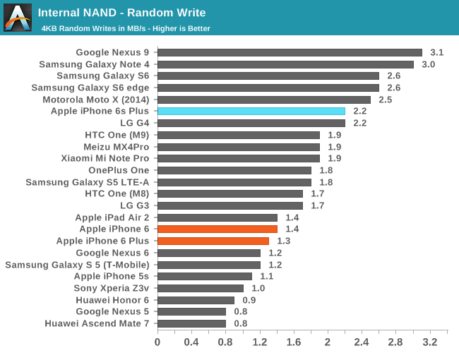
The graph is a bit difficult to interpret, but in effect we’re looking at the time it takes to write 256KB at a time until we get to 5GB. There are two notable spikes roughly around 2GB, but it appears to be small and likely to be some kind of garbage collection or some background work. At 3GB or so the latency increases which suggests that the SLC cache is overrun and write bandwidth is limited by TLC NAND performance.
Overall, NAND performance is impressive, especially in sequential cases. Apple has integrated a mobile storage solution that I haven’t seen in any other device yet, and the results suggest that they’re ahead of just about every other OEM in the industry here by a significant amount.
Storage aside, the SoC itself sees major changes this year. Apple has moved to a FinFET process from either TSMC or Samsung for the A9 SoC. However, it still isn’t clear whether the A9 is single source from one foundry or if A9 is being dual-sourced. Chipworks has reason to believe their iPhone 6s' A9 is fabricated on Samsung's 14nm process, though it hasn't been confirmed yet. Dual-sourcing is well within Apple's capabilities, however TSMC's 16nm and Samsung's 14nm process are not identical - naming aside, different processes developed by different fabs will have different characteristics - so dual-sourcing requires a lot more work to get consistent chips out of both sources. For what it's worth A8 was initially rumored to be dual-sourced as well, but decapping by Chipworks only ever turned up Samsung chips.
Moving on, let's talk about initial performance and battery life measurements, which look promising. Of course, it’s worth noting that the web browser benchmarks we currently have are often optimization targets for OEMs, so web browser benchmarks seen here aren’t necessarily evidence that the browser experience will be performant and smooth across all scenarios.
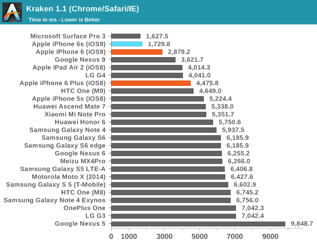
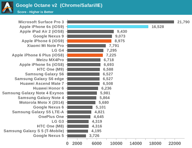
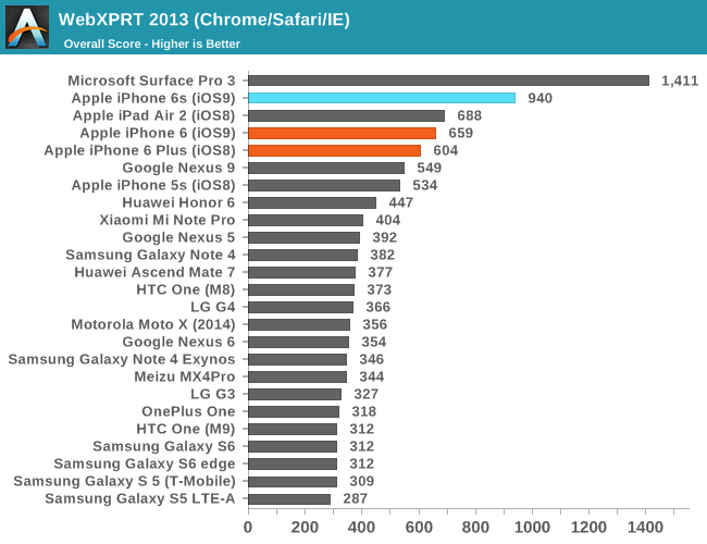 Regardless of whether an OEM is optimizing specifically for these benchmarks, it’s hard to ignore just how well Apple has optimized Safari and the dual core Twister CPUs as they’ve effectively set new records for these benchmarks in mobile. Of course, to try and really figure out the relative performance between CPU architectures when ignoring differences in operating system and developer convention we’ll have to turn to some of our native benchmarks such as SPEC CPU2000, but this will have to wait for the full review. What we can look at are some of our standard benchmarks that test graphics and game-related performance.
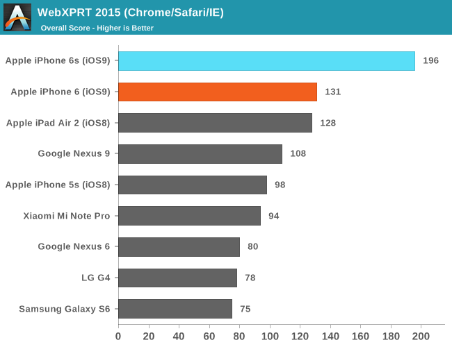
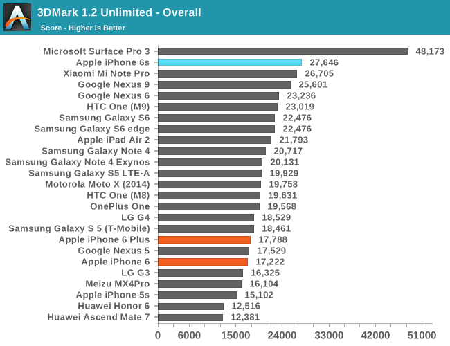
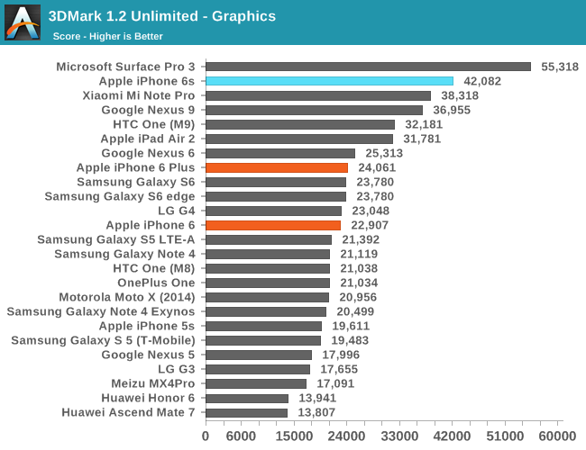 In 3DMark, we see the continuation of a long-running trend in the physics test in which the primary determinant of performance is clock speed and memory performance as data dependencies mean that much of the CPU’s out of order execution assets go unused. However, in graphics we see an enormous improvement, to the extent that the A9’s PowerVR GPU is actually beating the iPad Air’s GXA6850 GPU by a significant margin.
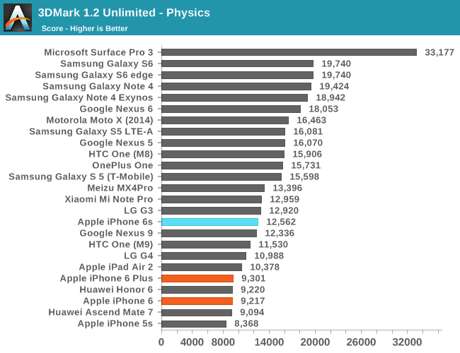
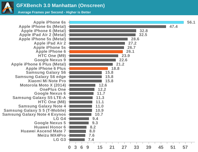
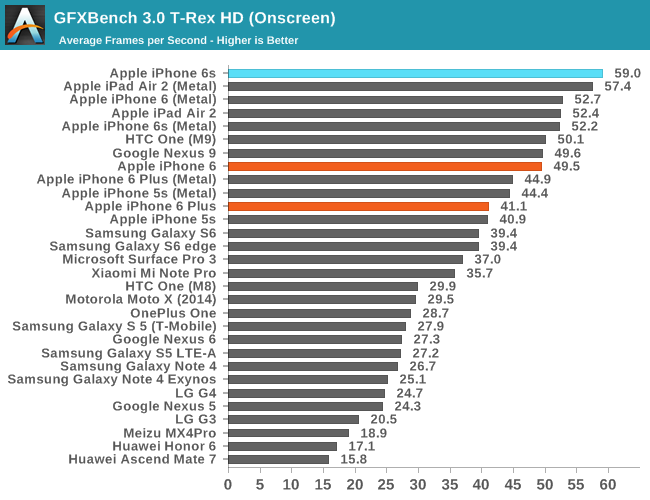
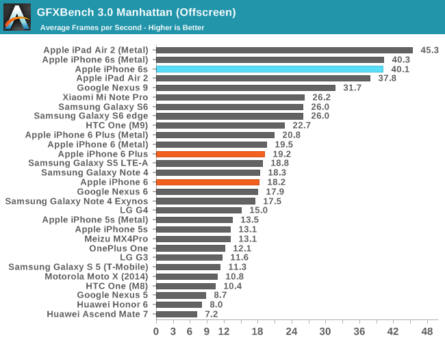 In GFXBench, we see a similar trend which is incredible to think about. Apple has managed to fit a GPU into the iPhone 6s that is more powerful than what was in the iPad Air 2 for OpenGL ES, which is really only possible because of the new process technology that enables much lower power consumption and higher performance.
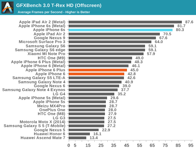
While I don’t normally call attention to most of the GFXBench subtests, in this case I think the driver overhead is worthy of special attention as it highlights one of the real-world benefits that improved CPU performance has. While we often think of CPU and GPU performance as orthogonal, the GPU is fundamentally tied to CPU performance to a certain extent as traditional APIs like OpenGL ES can have significant CPU overhead, especially as GPU performance has grown far faster than CPU performance. For APIs like OpenGL ES, to set up a frame it’s necessary for the CPU to check that the API call is valid, then do any necessary GPU shader or state compilation and begin running code on the GPU at draw time, which incurs increasing overhead as scenes become more complex. Through a combination of efficient drivers and enormous CPU performance, the dual core Twister CPU manages to set a new record for OpenGL ES driver overhead.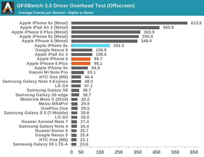
The final piece of data I've been able to collect over the course of the past few days is basic WiFi battery life. For those that are unfamiliar with the changes from the iPhone 6 line to iPhone 6s, the iPhone 6s now has a 1715 mAh (6.517 WHr) battery, and the iPhone 6s Plus has a 2750 mAh (10.45 WHr) battery. Both have a battery about 5.5-6% smaller than the previous generation.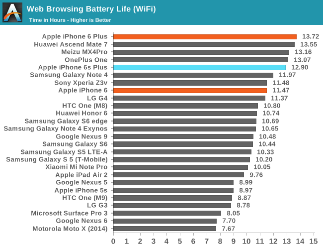
Interestingly, the iPhone 6s Plus appears to actually have accordingly less battery life at 12.9 hours, or right around 6% less than the iPhone 6 Plus. This could be evidence that there haven't been any efficiency improvements to the iPhone 6s line, but given that our testing shows Apple is already at the point where our web browsing test is effectively a pure display rundown it's likely we're looking at the worst-case difference. This warrants additional investigation, but it's possible that a more balanced workload will even out the difference in battery life and maybe even tilt the scales back towards the iPhone 6s depending upon how much load is placed on the SoC.
Overall, while there’s still a great deal of work left to do to exhaustively evaluate the iPhone 6s and 6s Plus, the initial results are quite positive. I haven’t finished a detailed investigation into the architecture of Twister, but I suspect we’re looking at some pretty significant changes compared to Typhoon, which would be unlike the smaller move from Cyclone to Typhoon. The GPU improvements are enormous, and while we don’t have enough data to determine whether the iPhone 6s retains the same sustained GPU performance that we saw in the iPhone 6, the peak performance figures are impressive to say the least. The SSD-like storage solution is also a major surprise, and likely to be overlooked as its effects are often hard to distinguish without direct comparison. Battery life does regress in a single test, but I suspect in real-world situations with less of a focus on the display battery life will either be equal or favor the iPhone 6s, so it will be interesting to see if Apple's battery life estimates remain as accurate as they traditionally have been. We’ve definitely discovered much more about the iPhone 6s than what we’re able to cover in this initial article, so stay tuned for the full review.
More...
-
09-28-15, 02:30 PM #5375
Anandtech: LG Steps Into The Ultrabook Ring With the LG Gram Series
LG has announced several new Ultrabooks labelled under the Gram series. They are going for a very lightweight and portable design, hence the name. There will be two models, with a 13.3-inch and 14-inch available starting today.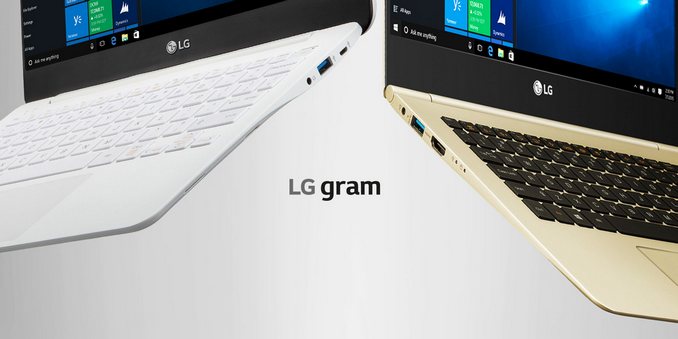
Both models feature a 1920x1080 IPS display, and weigh in at just 980 grams for either model, so there is no weight penalty going with the larger device. They are just 0.5” or 12.5mm thick, so they should have no issues with portability. The chassis are made out of carbon-lithium and carbon-magnesium which should result in a pretty strong frame despite the light weight and thin dimensions. LG has also managed to go with a minimal bezel of just 7.2mm on the sides, much like the Dell XPS 13, but they have kept a top bezel in order to fit the webcam. The 13.3-inch version will be offered in white, while the 14-inch version will be gold.
 LG Gram 13Despite being very thin and light, both models will be offered with Intel’s 15w processor lineup. The base offering is the Broadwell Core i5-5200U which is 2.2 GHz and a turbo to 2.7 GHz, and the 14-inch model will also be offered with the Core i7-5500U which is 2.4 GHz to 3.0 GHz. Memory is 8 GB of DDR3L which is listed as single channel, but being soldered on it could actually be dual-channel and only hands on with the device could determine that. Storage is 128 GB of SSD, with the i7 model doubling that to 256 GB.
There is HDMI, dual USB 3.0, and a SDXC card reader as well which should be enough for most tasks, and there is also a micro USB connector which can be used with the included 10/100 Ethernet adapter. It would have been nice to see Gigabit here, but that can’t work on a micro USB port and LG must not have wanted to tie up one of the USB 3.0 ports. Wireless is provided by the Intel Dual Band Wireless AC-7260 wireless card, but I would have preferred to see the 7265 model here.
 LG Gram 14Packing all of this into a small frame, light weight, and thin device is a pretty nice feat, but the one thing that seems to have taken a hit is the battery. LG rates both models at 7.5 hours of use, but the battery is just a 35 Wh model so it has a pretty big disadvantage over other Ultrabooks.
Perhaps most importantly, the LG Gram series will be sold through the Microsoft Store, which means they will be sold as “Signature PCs” from Microsoft. This means that there will be no extra software installed out of the box other than necessary utilities to function with the hardware. When you see the state of some PCs sold, with so much software installed that it would take you hours to clean it all off, this is a nice benefit and well done to LG for going down this route.LG Gram LG Gram 13 LG Gram 14 Processor Intel Core i5-5200U
2.2-2.7 GHz 14nm
15W TDPIntel Core i5-5200U
2.2-2.7 GHz 14nm
Intel Core i7-5500U
2.4-3.0 GHz 14nm
15W TDPMemory 8GB DDR3L GPU Intel HD 5500 Gen 8 Display 13.3" 1920x1080 IPS 14.0" 1920x1080 IPS Storage 128 GB SSD 128-256 GB SSD I/O 1 x micro USB
1 x HDMI
1 x SDXC
2 x USB 3.0Dimensions (mm) : 302 x 213 x 12.5
(inches) : 11.9 x 8.4 x 0.5(mm) : 325 x 226 x 12.5
(inches) : 12.8 x 8.9 x 0.5Weight 980 g / 2.16 lbs Battery 35 Wh, up to 7.5 hours Price $899 $999-$1399
The LG Gram is available starting today.
Source: LG
More...
-
09-28-15, 06:30 PM #5376
Anandtech: Apples A9 SoC Is Dual Sourced From Samsung & TSMC
Picking up from our conversation this morning on Apple’s A9 SoC, the crew over at Chipworks has been working hard over the weekend to decap A9 and their first results are in. As it turns out, Chipworks has found chips fabbed by both TSMC and Samsung, which means that A9 is in fact a dual sourced part.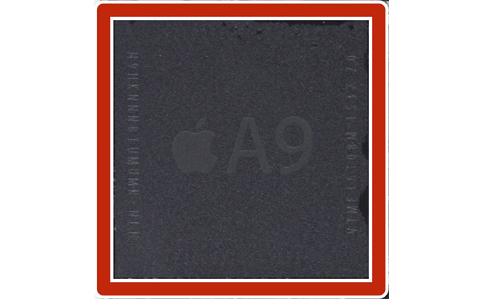
In taking apart iPhones and decapping SoCs, Chipworks has turned up two SoCs. The first, APL0898, is a 96mm2 A9 that’s fabbed by Samsung. The second SoC, APL1022, is a 104.5mm2 SoC fabbed by TSMC. And while Chipworks isn’t naming the specific manufacturing processes used, based on Apple’s comments on a “new transistor architecture,” we’re certainly looking at a form of FinFET. In which case the two chips are made on versions of Samsung’s 14nm FinFET and TSMC’s 16nm FinFET processes respectively.
This development is interesting for a few different reasons. From a fabrication standpoint, Samsung and TSMC have been brawling at multiple levels (technical and legal) to be the first to get a next-generation FinFET process out the door, with Samsung ultimately winning that battle when they shipped the 14nm Exynos 7420 for the Galaxy S6 family. For TSMC on the other hand this is as far as we know the first consumer product released with a 16nm TSMC fabbed part, indicating that TSMC is finally able to ship such parts in a reasonable volume.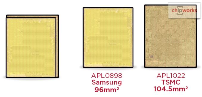
More importantly, this is a huge move for Apple, and one we admittedly don’t have all of the facts about at this time. Dual sourcing parts is by no means a new concept – IBM requiring a second source of x86 chips is how AMD got started in the x86 industry, after all – but in more modern times dual sourcing of high performance parts is very rare due to how difficult and expensive it is. With dual sourcing essentially requiring the chip to be taped out twice – once for each fab – it requires significant financial and engineering resources, a cost that not very many companies besides Apple can take on without significant risk.
The big hurdle with dual sourcing a part such as a cutting-edge SoC like A9 is that unless the source fabs have designed their processes to be near identical – to form a common foundry specification – then different fabs will have different processes with different characteristics. This in turn is determined by the technical decisions a fab made in research and development, and the specific issues the fab ran into when bringing up the new process. The end result being that while two fabs can turn out chips based around the same design, those chips will not be identical. It’s this kind of inconsistency that chip customers like Apple have to tackle head-on if they want to go with dual sourcing.Apple A9 SoC Versions APL0898 APL1022 Manufacturing Process Samsung 14nm FinFET TSMC 16nm FinFET Die Size 96mm2 104.5mm2
Even at a physical level we can see this inconsistency right away in terms of die sizes. Despite the TSMC and Samsung processes being quite similar, the Samsung A9 is the smaller of the two by 8%, which as Chipworks notes is indicative of better density on Samsung’s 14nm node. What we don’t see, and the issue Apple really has to control for, is power consumption. Right now it’s a safe assumption that both chips can reach Apple’s required clockspeeds, so in order for Apple to utilize both in the iPhone 6s they need to make sure both perform as identically as possible, especially when it comes to idle power leakage and power consumption at different clockspeeds. The billion dollar question right now is whether either of the A9s is consistently better than the other one, and in which case by how much. For Apple it’s best that these chips are identical as possible – and they can make design choices when tapping out the chip for each fab to help ensure this – but at the end of the day even Apple has to bow down to the laws of physics.
But the biggest unknown right now is why Apple would do this given the difficulties involved; to develop two A9s at twice the price. We can certainly speculate on reasons they would do this – yield issues at a fab, a desire to avoid putting all of their eggs in one basket and giving one fab too much power, or even just wanting to ramp up A9 production quickly by doubling the number of fabs working on it. But at the end of the day I don’t expect that’s a secret that will be known beyond the halls of One Infinite Loop, so speculation is all we have to work with for now.
In any case, if Apple has done their homework then dual sourcing A9s shouldn’t have an impact on average consumers, beyond perhaps ensuring that Apple has a sufficient supply to meet demand (ed: Apple sold 13mil iPhones in their opening weekend). Otherwise for techies, things are both more interesting and frustrating; just dual sourcing A9 makes an interesting product since this is something we almost never see done these days. As for the billion dollar question of which A9 is better, that will be a tossup. With enough time, effort, and a very large number of iPhones, it should be possible to coarsely determine if the A9s significantly differ in battery life, and thereby power consumption. However given the difficulties in taking an iPhone apart to access the A9, one would really need a software identification method to really make use of this information.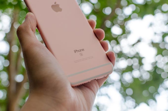
More...
-
09-29-15, 01:02 AM #5377
Anandtech: AMD Releases Catalyst 15.9 Beta Drivers
Today AMD has released AMD Catalyst 15.9 Beta as their latest driver update, with display driver version 15.201.1151. This driver provides optimizations for the upcoming Star Wars: Battlefront Beta that we will be seeing next week and for the Fable Legends DX12 benchmark that we saw last week.
Among several of the fixes a few of note are an issue with the AMD Catalyst Control Center 'update' option failing to download the latest driver, so users should now be able to properly update their drivers from within Catalyst Control Center. Also some BenQ 144Hz monitors were having driver issues by losing the video signal while uninstalling the driver and some BenQ 144Hz Freesync monitors would crash during DiRT Rally when launched in DirectX11 mode.
A couple of noteworthy known issues remain. For those running AMD Crossfire that are looking forward to the Star Wars: Battlefront Beta there is apparently a chance of some flickering happening, which is unfortunate. Also while booting into Windows 10 there can be issues with a black screen though the system will still continue on to the login screen. Lastly a TDR error (a.k.a. a driver crash) may happen while toggling between minimized and maximized mode while viewing 4K YouTube video content.
Those interested in reading more or installing the drivers for AMD's desktop, mobile, and integrated GPUs can find them on AMD's Catalyst beta download page.
More...
-
-
09-29-15, 03:30 PM #5379
Anandtech: Hands On With the Nexus 5X and 6P
Today Google announced several new devices at their September 2015 launch event in San Francisco. By far the most anticipated devices were the two new Nexus phones that were announced. The first is the Nexus 5X made by LG, a successor to the Nexus 5 which was released nearly two years ago in late 2013. The second is the Nexus 6P, which is made by Huawei and replaces the existing Nexus 6 made by Motorola. Both of these phones bring significant improvements over their predecessors, particularly the Nexus 5X which can take advantage of all the advancements made in the past two years. Below you can see the specifications for each of these new devices along with the specs of their predecessors to see how they compare.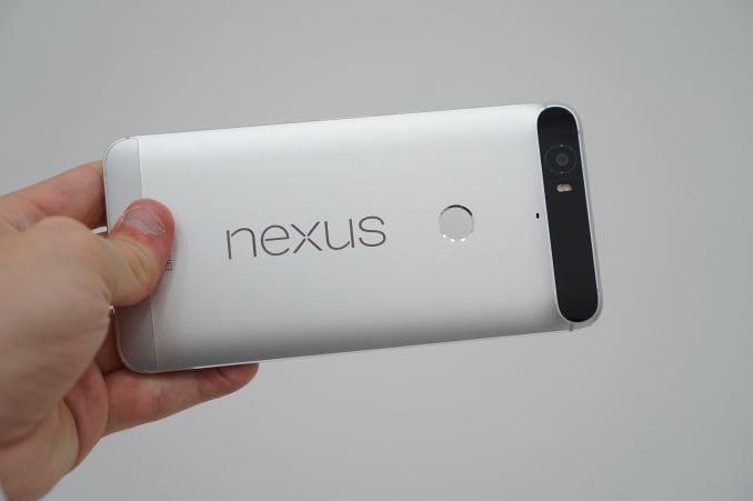
The Nexus 5X is similar to the Nexus 5 in some ways but different in others. The chassis is noticably thinner, although the camera protrudes a fairly significant amount. The device has gotten larger in the other dimensions as a result of its larger display. However, it's not that much larger, and during my time with it I never felt that it was difficult to hold. The SoC moves from Qualcomm's Snapdragon 801 to Snapdragon 808, with the amount of RAM and internal NAND remaining the same. The battery capacity receives a significant bump, going from 8.74Wh to 10.26Wh. As for the camera, it's greatly improved. The Nexus 5 was never known for having an amazing camera, and with these new Nexus phones Google appears to have implemented a custom camera sensor. It's a 12.3MP sensor with 1.55 micron pixels, which roughly equates to a 1/2.3" sensor format.Google Nexus Smartphones LG Nexus 5 LG Nexus 5X Motorola Nexus 6 Huawei Nexus 6P SoC Snapdragon 800 Snapdragon 808 Snapdragon 805 Snapdragon 810 GPU Adreno 330 Adreno 418 Adreno 420 Adreno 430 RAM 2GB LPDDR3 3GB LPDDR3 3GB LPDDR4 Display 5.0-inch 1920 x1080 IPS LCD 5.2-inch 1920 x 1080 IPS LCD 5.96-inch 2560 x 1440 AMOLED 5.7-inch 2560 x 1440 AMOLED Wireless 1x1 802.11a/b/g/n/ac BT 4.2, NFC 2x2 802.11a/b/g/n/ac BT 4.2, NFC Storage 16/32GB 32/64GB 32/64/128GB I/O microUSB, 3.5mm audio USB Type-C, 3.5mm audio microUSB, 3.5mm audio USB Type-C, 3.5mm audio Size / Mass 137.84 x 69.17 x 8.59mm, 130g 147.0 x 72.6 x 7.9 mm, 136 grams 159.26 x 82.98 x 10.06mm, 184g 159.3 x 77.8 x 7.3mm, 178 grams Battery 2300 mAh (8.74Wh) 2700mAh (10.26Wh) 3220 mAh (12.236Wh) 3450mAh (13.11Wh) Camera Rear Facing 8MP, 1/3.2", (Sony IMX179), F/2.4
Front Facing
1.3MPRear Facing
12.3MP with 1.55µm pixels, F/2.0
Front Facing
5MP, F/2.0, 1.4µmRear Facing 13MP, 1/3.06" (Sony IMX214), F/2.0.
Front Facing
2.1MPRear Facing
12.3MP with 1.55µm pixels, F/2.0
Front Facing
8MP, F/2.0, 1.4µmSIM MicroSIM NanoSIM Launch Price $349 (16GB) $379 (16GB) $649 (32GB) $499 (32GB)
The back of the Nexus 5X feels similar to the material used in the black Nexus 5. There's also a blue model and a white model, and while I didn't get to try the white model the blue version seemed to have the same texture as the black one. The design of the phone diverges significantly from the appearance of the Nexus 5. There's no more raised black ring around the camera, which makes the current Nexus 9 a bit of a loner as it's the only device left that has that design accent. The camera has also been moved to the center of the back, while on the Nexus 5 it was situated in the upper corner. Something worth noting is that the Nexus 5X and 6P both lack OIS, something that existed on their predecessors. Google's rationale is that you won't need long exposures as the camera sensor and pixel size is large enough to work well without it. Whether or not that is true remains to be seen, but OIS is still a useful feature and I think many users who are hoping to upgrade from an existing Nexus smartphone will be sad to see it gone.
On the software side, Android Marshmallow has a significantly improved camera app. Google has addressed many of the issues with menus and settings being difficult to find, and I also noticed that the camera preview frame rate on the Nexus 5X and 6P was much higher than on the Nexus 5 and 6.

Below the camera is Google's new fingerprint sensor. According to Google it can recognize a finger in under 600ms and has a very low error rate. It's difficult to say how it compares to other devices, and I wasn't able to get time to use it, so that will have to wait for when we actually review the Nexus 5X. The position on the back seems to be well chosen, and because it also will wake up the phone it doesn't suffer from the issue with some early rear-mounted fingerprint scanners which is that you had to wake the device first.

As for the front of the phone, there's not a whole lot to say. It's dominated by the display, with the earpiece on the top and a single speaker on the bottom and a front-facing camera to the left of the top speaker. The display itself seemed very good, and the color rendition looked similar to the Nexus 5 which is a good sign. While the Nexus 6P has an AMOLED display, the Nexus 5X is an IPS LCD.

Next is the Huawei-made Nexus 6P. Every aspect of the device feels like a large improvement over the Nexus 6. The first thing that stood out to me is the size. The Nexus 6 was extremely large and I couldn't hold it properly in really any circumstance. The Nexus 6P takes a step back to a 5.7" display, and the dimensions of the phone itself are not much larger than the iPhone 6s Plus despite the larger screen. Of course, you end up losing some real estate to the on screen buttons while the iPhone has a physical home button, but the point is that the phone is much easier to hold and use than the Nexus 6 was. The thickness also contributes to this as well, as the Nexus 6P is almost 3mm thinner than the Nexus 6.
Beyond the dimensions, the construction and feel of the phone is miles ahead of the Nexus 6. It's an aluminum unibody construction with a diamond cut edge edge, and the primarily plastic construction of the Nexus 6 isn't even remotely comparable. It's also fairly light considering the aluminum build and its size.

Something worth noting is that Google seems to have given Huawei and LG a lot of freedom when designing these new phones. The Nexus 5X doesn't share many visual characteristics with the 6P apart from the Nexus logo on the back and the fingerprint scanner. Rather than mounting the camera in the middle, Huawei has put it in the upper left corner like the old Nexus 5 did. The entire top of the back also has a slightly raised black bar. I'm honestly not a fan of this, as it just interrupts what should be a continuous aluminum surface.
Like the Nexus 5X, there's not a whole lot to say about the front of the Nexus 6P. It has stereo speakers, a front-facing camera, and a large display. The 6P bumps the front camera resolution up to 8MP from the 5X's 5MP, with a corresponding increase in sensor size to maintain the 1.4 micron pixel size.
The display is the part of the Nexus 6P that I was most curious about. The Nexus 5 was notable for having a very accurate display despite its low price, and with the Nexus 7 also having accurate calibration it was hoped that Google would continue this across all of their products. Unfortunately, the Nexus 6 shipped with a very poorly calibrated AMOLED display with low brightness. When I first used the Nexus 6P I was very upset to see that it was clearly oversaturated like the Nexus 6, but there's more to the story this time around. In the Nexus 6P's developer settings there is a switch to enable an sRGB mode, and when this switch is turned on the Nexus 6P's display appears to have similar color rendition to the Nexus 5X which is a very good sign. While we'll need to get a review unit in order to analyze all of the display's attributes, I am hopeful that Google has recognized and fixed the issues with the Nexus 6's display in the Nexus 6P.

On the bottom of the Nexus 5X and Nexus 6P you'll find a 3.5mm audio jack but you won't find a USB Micro-B port. Google has decided to be forward looking, and like the Chromebook Pixel the new Nexus smartphones use the USB Type-C connector for data and charging. While this will come with some pain in the short run as users won't be able to use existing USB Micro-B cords, I think the benefits are worth it.
Both new Nexus devices also come with the new Android Sensor Hub. This essentially refers to the different sensors that the devices include, and how they are now controlled and managed by a dedicated processor rather than the device's application processor. This is important for features like Doze in Android Marshmallow, as it allows Google to use minimal power to check the status of sensors and determine whether or not to go into deep sleep.
For me personally, the Nexus 5X is the most interesting of Google's two new Nexus phones. I always like to see what vendors can do when they're targeting a price far less than that of a flagship smartphone. The Nexus 6P definitely has its appeal too though, and we'll be running both of them through our standard suite of tests in order to see how they compare to the competition. If you're already convinced that you want the Nexus 5X or 6P you can pre-order them online now from the Google Store so long as you live in the US, UK, Canada, Japan, or Ireland. The Nexus 5X starts at $379 and comes in black, white, and blue, while the Nexus 6P starts at $499 and comes in standard aluminum, white, and black.
More...
-
09-29-15, 04:31 PM #5380
Anandtech: HTC Launches the One M9+ Supreme Camera Edition
Today, HTC launched the One M9+ Supreme Camera Edition. The rather verbose and mildly surreal name probably gives away what this phone is, which is a variant of the One M9+ with some significant changes to the camera. The spec sheet below should give a pretty good idea for what to expect.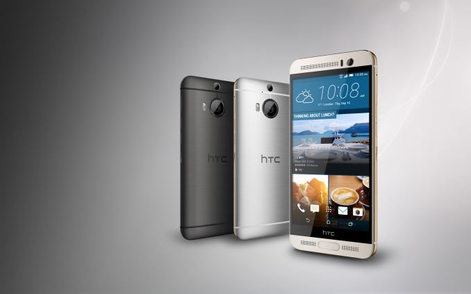
As you can see, the big change here is the camera. Instead of the 2.1MP secondary camera, HTC has added an IR laser rangefinder for short distances, which should dramatically speed up auto-focus in low light and macro shots. The sensor is now a Sony IMX230 with phase detect auto focus, so in conditions with good light it should be possible for the sensor to traverse straight to in-focus instead of bracketing the in-focus point with contrast detection. However, the optical characteristics are unchanged from the One M9 and M9+ with an f/2.2 aperture likely to keep edge distortions under control. OIS is also added to improve low light performance for still photos and improve video stability.HTC One M9+ HTC One M9+ Supreme Camera Edition SoC MT6795 2.2GHz 8xA53 MediaTek Helio X10 MT6795 2.2GHz 8xA53 MediaTek Helio X10 RAM/NAND 3GB LPDDR3
32GB NAND + microSD3GB LPDDR3
32GB NAND + microSDDisplay 5.2” 1440p IPS LCD 5.2” 1440p IPS LCD Network 2G / 3G / 4G LTE (MediaTek Category 4 LTE) 2G / 3G / 4G LTE (MediaTek Category 4 LTE) Dimensions 150.99 x 71.99 x 9.61mm 168g 150.99 x 71.99 x 9.61mm 168g Camera 20MP Rear Facing w/ 1.12 µm pixels, 1/2.4" CMOS size, f/2.2, 27.8mm (35mm effective)
2MP Duo cam
4MP Front Facing, 2.0 µm pixels, f/2.0 26.8mm (35mm effective21MP Rear Facing w/ 1.12 µm pixels, 1/2.4" CMOS size, f/2.2, 27.8mm (35mm effective)
Laser AF + PDAF + OIS
4MP Front Facing, 2.0 µm pixels, f/2.0 26.8mm (35mm effective)Battery 2840 mAh (10.79 Whr) 2840 mAh (10.79 Whr) Connectivity 802.11a/b/g/n/ac + BT 4.1, GNSS, NFC, DLNA, microUSB 2.0 802.11a/b/g/n/ac + BT 4.1, GNSS, NFC, DLNA, microUSB 2.0 SIM Size NanoSIM NanoSIM
The One M9+ Supreme Camera edition will go on sale in Taiwan on October 6th for $630 USD in gunmetal grey and two-tone silver/gold. This is likely to remain an Asia-only variant, although we may see a similar camera in future devices.
More...


 Quote
QuoteThread Information
Users Browsing this Thread
There are currently 19 users browsing this thread. (0 members and 19 guests)


Bookmarks