

Results 5,661 to 5,670 of 12096
Thread: Anandtech News
-
01-17-16, 07:09 AM #5661
Anandtech: G-Technology Demonstrates G-SPEED Shuttle XL Thunderbolt 2 DAS at CES
As part of every CES trip, I make it a point to visit G-Technology and see what they are introducing into the DAS (direct attached storage) market. This year, there were no major announcements except for the introduction of a Type-C interface for some of their external hard drives. These are still USB 3.0 drives, as there is not much to gain by moving to a USB 3.1 interface for hard drives. However, it must be noted that these 2.5" drives are 7200 RPM ones providing that extra bit of performance compared to the 5400 RPM drives used by most vendors. G-Technology expects the 1TB version to have a MSRP of $130 when it launches in February.
Coming back to the more impressive part of my visit to the suite, G-Technology showed the various features of the G-SPEED Shuttle XL. This 8-bay hardware RAID solution comes with two Thunderbolt 2 ports. The platform itself is very similar to the G-SPEED Studio XL introduced by G-Technology at IBC 2015 in September. This product also has two ev Series Bay Adapters which enable support for the G-DRIVE ev modules. These modules can easily be swapped across different interface modules for use in rugged environments, or just for portability, or even with high-capacity arrays like the G-SPEED Studio / Shuttle XL.
The Shuttle XL can be oriented either vertically or horizontally. In the horizontal configuration, it can even be used as a stand for the notebook (to which it may connect). G-Technology also has an adapter for a RED MINI-MAG so that it can be read into the computer directly through the Shuttle XL. A RED MINI-MAG and a G-DRIVE ev SSD are shown connected to the Shuttle XL using the two ev Series Bay Adapters in the above picture. The Shuttle XL also has a custom-designed transportation case for portability across different work locations.
Claimed transfer rates are around 1350 MBps. The disks can be configured in RAID 0,1,5,6,10 and 50. The unit is sold with enterprise-class hard drives with pricing ranging from $3500 for 24TB to $8000 for 64TB. G-Technology provides a 3-year warranty for the product.
We saw LaCie launch a 8-bay Thunderbolt 2 1U rackmount unit, the 8big Rack Thunderbolt 2 a couple of years back. It is interesting to see G-Technology have a 'portable' take on the8-bay hardware RAID Thunderbolt 2 enclosure market. From an end-user perspective, it is great to have both choices and one can let the usage model dictate the suitable solution.
More...
-
01-17-16, 03:34 PM #5662
Anandtech: Amped Wireless Launches APOLLO IP Cameras and Updates Networking Lineup at
Amped Wireless is popular for marketing equipment with long range, high-performance power amplifiers and high-gain antennas. At CES, they had the usual updates to the networking lineup - new Wi-Fi routers and range extenders. In addition, they also announced their entry into the IP camera space with two Wi-Fi cameras.
The APOLLO IP Camera Lineup
The lineup consists of two members, the APOLLO and the APOLLO PRO. They both have wireless capabilities. Amped Wireless claims that these models can be placed 3x the distance away compared to the average Wi-Ficamera. While the APOLLO will have a 80 degree viewing angle and a 1-way microphone, the APOLLO PRO will have a 110 degree viewing angle and 2-way microphone and speaker. Both cameras have a 720p resolution and night vision is available. The external 3.5dBi antenna is detachable on both models.
The setup as well as day to day operation is geared towards the average consumer by the usage of mobile apps and a cloud recording backend. The cameras are priced at $150 and $180 respectively, and will be available towards the end of this quarter.
ARTEMIS AC1300 Family
The ARTEMIS lineup of networking products includes a router, range extender (ARTEMIS-EX) and an access point (ARTEMIS-AP). Priced at $130, these products come with up to 5 GbE ports and a USB 3.0 port. MU-MIMO is supported out of the box, pointing to a Qualcomm Atheros platform.
Based on the specifications and the cost, it appears that the product line uses the IPQ40x8/x9 SoC.
ATHENA AC2600 Family
The ATHENA lineup includes the ATHENA-R2 router and the ATHENA-EX Wi-Fi extender, both with advanced MU-MIMO capabilities. Compared to the first generation MU-MIMO routers, this device can support up to four simultaneous MU-MIMO clients. It also supports 160 MHz channels.
Based on the specifications, it appears that the units are based on the QCA9984 radio. The SoC is not clear - as the brochure given to the press indicates a 1.3 GHz quad-core processor for the router (RTA2600-R2) and a dual-core processor for the range extender (RE2600M). Note that the Nighthawk X4S from Netgear which has the QCA9984 radio uses a 1.7GHz IPQ8065 SoC. The ATHENA router will be priced at $240, while the extender will be $220 when they launch at the end of this quarter.
REC22P Range Extender
This is an interesting product in the sense that it bundles a rapid charging USB Type-A port as well as a passthrough power outlet in the device. The range extender effectively doesn't use up a wall outlet. It is a AC1200 device (867 Mbps in the 5 GHz and 300 Mbps in the 2.4 GHz - a 2x2 configuration).
The REC22P will be available in late February for $100.
The specifications of the various routers, access points and range extenders currently marketed by Amped Wireless are reproduced from the press brochure in the gallery below.
Gallery: Amped Wireless Q1 2016 Product Offerings


On the whole, it is pleasing to see Amped Wireless trying to move beyond the core networking devices (such as routers / access points / range extenders) and on to allied products such as IP cameras. For mass acceptance, IP cameras need to be backed up by good user experience, and Amped Wireless seems to be focusing more on that rather than the hardware specifications alone. On the core side, Amped Wireless seems to be all in on the Qualcomm Atheros platforms for their flagship ATHENA lineup and the ARTEMIS value play.
More...
-
01-18-16, 07:34 AM #5663
Anandtech: New GIGABYTE Server Motherboards Show Xeon D Round 2
The Xeon D platform, as reviewed by Johan back in June, put together eight Broadwell cores, 24 PCIe 3.0 lanes, dual 10 Gbit Ethernet and USB/SATA control all into one SoC within a 45W TDP design. It almost sounded too good to be true (I’ve run some benchmarks my side, to be in a review later), as this is the only real way to get eight 14nm cores into a single die. Even at 2 GHz, Johan’s piece showed that the Xeon D based on Broadwell aims to fit between the Xeon E3 and Xeon E5 in terms of performance and power efficiency, and to quote Johan ‘Xeon D is probably the most awesome product Intel has delivered in years, even if it is slightly hidden away from the mainstream’. There is interest both server side and NAS side for this, and with the next wave of Xeon D parts being introduced GIGABYTE Server is one of the first to announce some new models.
Technically, the four motherboards being launched are a single base design, but with either a different SoC or different networking:
2 x 1 GbE +
2 x 10GbE SFP+2 x 1 GbEOnlyWith Xeon D-1541 MB10-DS3 MB10-DS0 With Xeon D-1521 MB10-DS4 MB10-DS1 The image above is the top end MB10-DS3 model, featuring the Xeon D-1541 processor with 8 cores, 16 threads, running at 2.1/2.7 GHz for base and turbo frequencies. This is a mini-ITX board aimed at the typical 1U chassis, with four RDIMM/UDIMM DDR4 slots for up to 128 GB RDIMM support in ECC or non-ECC fashion. As mentioned before, the differentiator on this model aside from the SoC is the networking, and here we get dual Intel I210-V gigabit Ethernet paired with dual Cortina CS4227 10GbE SFP+ LAN ports to either route teamed to an SFP+ switch or to different switches althogther.
The motherboard uses a single PCIe 3.0 x16 slot which can be used for compute, and storage comes via five SATA 6 Gbps ports and another similar port that also supports SATA DOM. With it being a server motherboard, the onboard Aspeed AST2400 provides an IPMI interface for management as well as a 2D acceleration video chip. There are two extra fan headers on board, as well as a USB 3.0 header and a TPM header.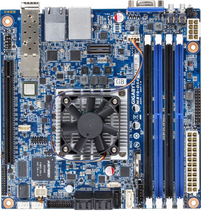
The SoC here has a list price of $581 on its own, and given that this is a server part I’m not too sure we will see these set of boards actually up at retail, although I do know that GIGABYTE Server is trying to push more product through that distribution channel. Businesses interested in the platform will have to enquire to their local GIGABYTE office to find out more information on pricing and availability.
As part of the second wave of Xeon D processors, Intel seems to be releasing a number of 35W and 45W models, from four cores to eight cores (with Hyperthreading), varying otherwise by speed and last level cache in-line with core count. I imagine that as more of these trickle through into the hands of OEMs, we will see more products through 2016.
More...
-
01-18-16, 09:56 AM #5664
Anandtech: D-Link Demonstrates Innovative Networking Solutions at CES
D-Link had two major core networking announcements at CES along with a host of updates for their home automation product line. There are a number of things to discuss with respect to the core networking announcements. So, I will get the minor home automation stuff out of the way first.
D-Link has been offering a set of home automation products with unified cloud-based control using the mydlink Home app. At CES, they announced the integration of the IFTTT (If-this-then-that) service with the app, allowing more customization in the home automation experience. It is slated to appear in the free app later this quarter. IFTTT integration has been a staple of many home automation products (including the Belkin WeMo) for some time now. So, it is good to see D-Link putting the effort to integrate with IFTTT with their own cloud back-end.
The other home automation-related announcement was a new product - a Wi-Fi based alarm detector. Simply put, this device plugs into a wall outlet and connects via Wi-Fi to the Internet. A microphone in the device is set to trigger an alarm if the sound of a smoke alarm or carbon monoxide alarm is heard. This allows legacy smoke and CO detectors to become part of the smart home - definitely more cost effective than installing completely new smoke alarms (like what Nest suggests). D-Link indicated that, in the future, it might also be able to make the microphones in their IP cameras do the same job.
Moving on to the core networking announcements, we first have the EXO series of routers. This series has two members, the AC1750 DIR-869 and the AC1900 DIR-879. Both have a 3x3 configuration in the 5GHz band for 1300 Mbps of theoretical bandwidth. However, the DIR-879 does 600 Mbps in the 2.4GHz band and the DIR-869 does 450 Mbps in the same. The DIR-869 will retail for $130 and the DIR-879 will retail for $150 when they go on sale later this quarter.
In order to achieve this lower price, D-Link has opted to not integrate a USB port on either model. Both have a hardware toggle switch to move between router and extender modes. However, the devices do have high-performance power amplifiers (1000mW). The interesting aspect here is the core platform. While vendors such as Amped Wireless have gone in for the integrated Qualcomm Atheros 2x2 solution for their $130-price point router, D-Link has moved to Realtek for the same. The SoC used is the RTL8198C with a 620 MHz MIPS-based dual-core host processor and 5 GbE ports integrated. The WLAN chips are RTL8814AR for the 5GHz radio and RTL8194AR for the 2.4GHz radio.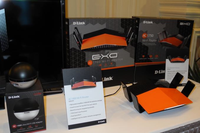
The most innovative demonstration in D-Link's suite was the Unified Home Wi-Fi Networking Kit with Adaptive Roaming Technology (DKT-891). This is a router-extender kit that will retail at $370when it launches in Q2. The DKT-891 consists of two products - the DIR-891L, an AC4300 tri-band MU-MIMO router, and the DAP-1655, an AC1300 gigabit Wi-Fi extender. The DIR-891L seems to be the first tri-band 4x4 router based on a Qualcomm Atheros chipset. With two 5GHz 4x4 radios, each band can support 1733 Mbps (for a total of 3466 Mbps). The 2.4 GHz band can support 800 Mbps with the 256-QAM feature. This gives a total bandwidth of 4266 Mbps, enabling classification as a AC4300 class router. The DAP-1655 provides 867 Mbps in the single 5GHz band and 450 Mbps in the 2.4GHz.
The Unified Home Wi-Fi Networking Kit with Adaptive Roaming is based on Qualcomm's Wi-Fi S.O.N technology (video). At their CES suite, D-Link demonstrated 'Smart Steering' - clients moving from the router to the extender automatically (depending on which one was providing a better signal). They also showed 'Dynamic Adaptation' - clients moving inbetween the 2.4 GHz and 5 GHz bands for load balancing purposes. All of this was done without any end-user intervention. Even though the demonstration looked market ready, it is likely that more 'interoperability' testing will be needed. Getting 'Smart Steering' and 'Dynamic Adaptation' to work across multiple client platforms will definitely be a challenge.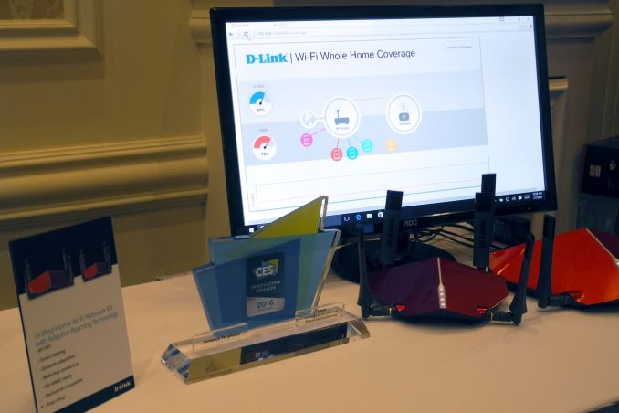
Gallery: D-Link at CES 2016


In addition to the above new announcements, D-Link also showed their currently-shipping Broadcom-based Ultra series of routers. the 3x3 DWA-192 USB 3.0 AC1900 WLAN adapter and some IP cameras (including the Komfy switch launched in November).
More...
-
01-18-16, 12:05 PM #5665
Anandtech: Supermicro Quietly Launches the C7Z170-OCE: Multi-GPU focused with PLX8747
One of the biggest changes to the motherboard scene since the release of Skylake is the distinct lack of motherboards designed to cater for more than two PCIe cards using CPU-based lanes. Back in the era of the Z77 chipset, I gathered four motherboards that had the PLX8747 PCIe switch installed, allowing for >2 GPUs, and we really went to town on the detail and benchmarking. But with Z170, the use of the this chip has severely diminished for two reasons. Firstly, GPUs are getting powerful enough to drive 1440p gaming by themselves fairly easily, and secondly, Avago bought PEX, the company that makes these switches, and the price for them essentially doubled overnight. As a result, only a few motherboards for Z170 will have them, such as the Z170-Gaming G1 we reviewed at the end of last year, because of the consumer price concerns and the market to which they are aimed. The GIGABYTE model we reviewed was $500, and featured all the bells and whistles such as Thunderbolt 3 – the Supermicro motherboard announced last week with this PLX chip is the C7Z170-OCE but slides in at $300.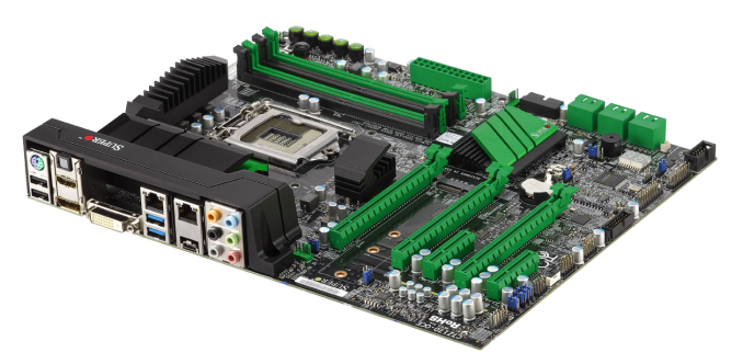
This motherboard aims to be ‘green’ in more than just the aesthetics. Supermicro’s value add to the community, and the part that they aim to be the differentiating factor, is their long standing role in the server space. They want to use this reputation to promote their use of server grade components on consumer platforms. This will come through in their regular consumer motherboard segments (such as the C7H170-M which we’ve nearly finished testing) and their gaming motherboard line, which now has a name: SuperO.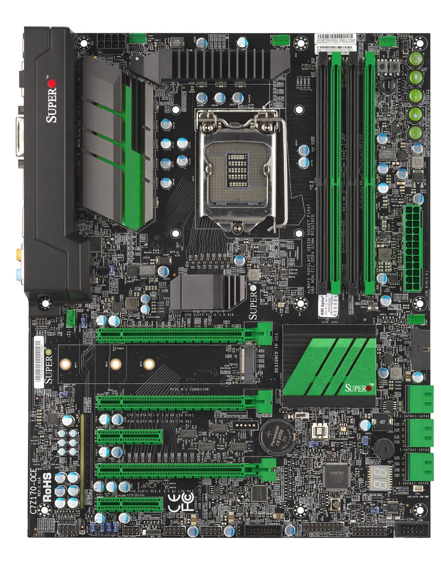
The C7Z170-OCE is aimed squarely at the three-GPU user on Skylake. The PLX8747 chip splits the PCIe lanes into x16/0/x16 or x16/x8/x8, leaving the chipset enough space to add in an M.2 slot for up to PCIe 3.0 x4 bandwidth and plenty of space on the bottom to make sure all the headers can still be used when dual slot cards are in play. We have tested the PLX8747 before, and found that the chip does not noticeably (sub-1%) reduce performance when in use. As SuperMicro is still feeling its way around the consumer motherboard space, we are seeing features that enthusiasts are used to being promoted as positive points. So for example this board also gets some buttons for pre-overclock modes in the top right, and promotes features such as ‘SuperFlash’ which other motherboards have had for almost half a decade. Nonetheless, the fact that these exist now is still a plus.
Audio is provided by a Realtek ALC1150, and networking via Intel I219-V and Intel I210-AT controllers. Due to the use of dual Intel controllers, Supermicro lists teaming, fail over and load balancing as features of this comvination. USB 3.1 is given on the rear in a Type-C configuration through the ASMedia ASM1142 controller, although it seems a little odd that only one port of this controller is being used. There is another ASM1142 onboard near the bottom, which is connected to a USB 3.0 header – the motherboard is advertised as having a USB 3.1 (10 Gbps) header, but this standard isn’t finalized so we are looking into whether Supermicro is actually validating this header at double the data rate than normal. (It turns out this header will support two USB 3.0 or one USB 3.1, but it requires the right connectors/ports which will not be included in the bundle.)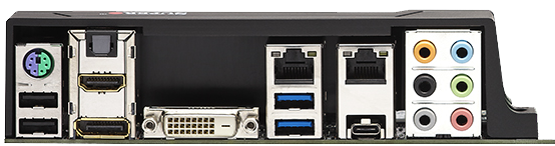
On the software side, our upcoming C7H170-M review will go into an interesting feature called SuperDoctor 5, which is a pseudo server-like web interface for motherboard features and monitoring.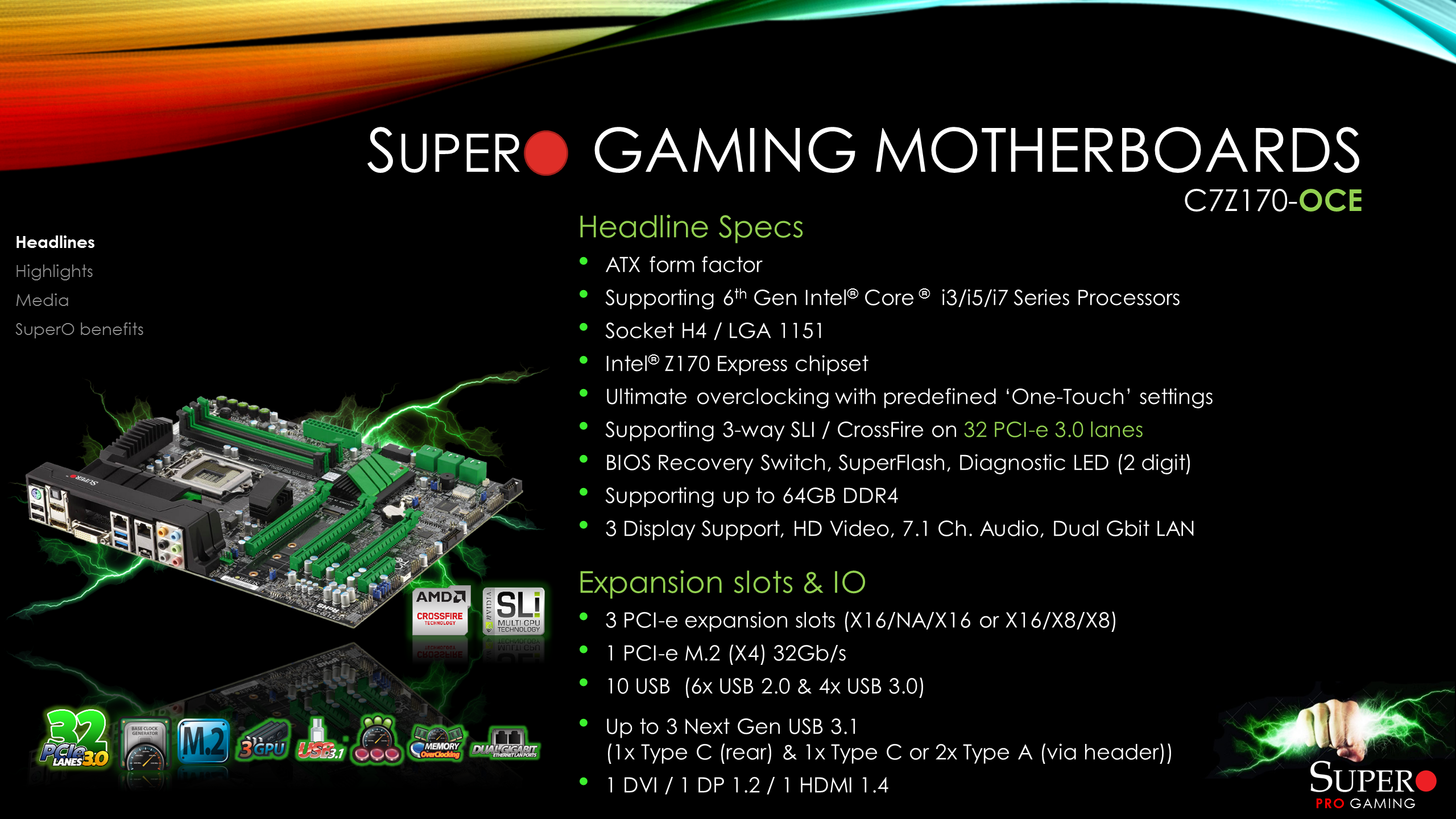
At this point, the C7Z170-OCE will be the cheapest tri-PCIe focused (both SLI and CrossFire) on the market for Skylake at $300. Also anyone wanting to build a green machine will love the aesthetic. I am told it should hit the shelves by the end of January.
Source: Supermicro
More...
-
01-19-16, 07:07 AM #5666
Anandtech: ECS Goes Skylake with LIVA One
At CES 2016, ECS displayed their consumer-focused as well as OEM products to the press and business customers. On the direct-to-consumer side, ECS had some 100-series chipset boards on display, but they were all ones that had been announced before (like the Z170-Claymore). However, my main intention was to check out updates to the LIVA mini-PC lineup and also get some information on the 5x5 form factor that ECS had hinted at prior to the show.
In our Intel Compute Stick review, we had talked about the efforts made by Intel to take advantage of a second screen (such as a tablet or smartphone) when interacting with the PC. ECS also had something similar for the LIVA series. They have tied up with Insyde Tools to install necessary support for ShareKanTan on the LIVA mini-PCs that come with the OS pre-installed. In addition to the input options provided by apps such as the Intel Remote Keyboard, this app also allows for display of media on the PC in the second screen.
ECS also took the opportunity at CES to show off their latest addition to the LIVA lineup - the LIVA One. LIVA One is a Skylake mini-PC, which uses a 35W TDP -T class processor. Unlike other members of the LIVA family, this one is larger (1L volume - 173mm x 176mm x 33mm) and also actively cooled. The default configuration from ECS utilizes a Core i3-6100T, a LGA processor. The end user can actually upgrade the CPU after purchase, or install any other CPU after buying a barebones configuration. Even processors such as the Core i7-6700T can be used (as long as the CPU is LGA1151 and has a TDP within 35W).
The LIVA One uses 2x DDR3L SO-DIMMs.It has a free 2.5" SATA drive slot and also a M.2 SSD slot (SATA interface). The industrial design is stylish and functional, with the front panel including a microSD slot and a USB 3.1 port (with rapid charging features). The default configuration contains a 1x1 802.11ac / BT 4.0 WLAN card, but that can be changed by the end user.
ECS has also used the same chassis design for a mini-PC to target business users. This 'SF100' model will support Windows 7 officially. It also supports vPro (thanks to the Q170 chipset) and Intel SBA (Small Business Advantage) technology. Unlike the LIVA One's DDR3L SO-DIMM slots, the SF100 has the costlier DDR4 SO-DIMM slots that can provide better RAM capacity and performance. It also has a RS-232 port as well as a 2W in-built speaker. The SF100 also uses an Intel I219-LM GbE NIC.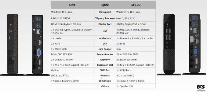
Both the LIVA One and the SF100 can be augmented with an optical drive or extra 2.5" bay using a special 'HD Drive Bay' (shown in the top picture) that connects to the main system via one of the rear USB 3.0 ports. The LIVA One will be priced $168 for the barebones configuration and $450 for the pre-built default configuration. Pricing for the SF100 is not available yet.
Moving on to the mini-STX front (the official name for the 5x5 boards that we first uncovered at IDF 2015), ECS had one of the first motherboards in this form factor on display. The H110SU-02 (with the S standing for the mini-STX form factor in ECS's nomenclature) is meant for SFF systems, thanks to the low-profile heat sink from Silverstone. ECS and Silverstone have tied up to offer consumers a one-stop shop for those attempting to build a system based on the H110SU-02 mSTX board. The gallery below shows some shots of the motherboard with a low profile heatsink installed.
Gallery: ECS H110SU-02 mSTX 5x5 Motherboard


The full details of the board are provided in the table below. Pricing is not available yet.
On the whole, the consumer products from ECS on display at CES point to where the desktop computing market is headed. The market share for small form factor systems is increasing even as the overall desktop PC market declines. SFF systems are also turning out to be an attractive proposition in the business PC market.ECS H110SU-02 Specifications Form Factor Intel mSTX Form Factor Chipset Intel H110/B150 Chipset
Intel i3/i5/i7/Pentium/Celeron Processors (65W)Memory 2x SO-DIMM DDR4 Networking 1 x M.2 Slot (2230) for WiFi/BT 4.0
1 x RJ45 1GbpsStorage 1 x M.2 Slot (2280) for SSD
1 x SATA support SSD or HDD or ODDDisplay 1 x HDMI 1.4a Output
1 x DP OutputAudio 1 x Audio Combo Jack External I/O 1 x USB 3.1 Type C (with EZ charger)
2 x USB 3.0 PortsDimensions 140(W) x 147(D) mm Power Supply DC-in 19V 90W OS / Driver Support Windows 7 / 8.1 / 10 / Linux
More...
-
01-19-16, 08:24 AM #5667
Anandtech: ASUS Booth Tour at CES 2016: 10G Switches, External GPU Dock, USB-C Monito
When ASUS emailed a couple of weeks before CES announcing that they had cancelled their press event for the show, we had a few question marks. Previous shows involve Chairman Jonney Shih’s rapid fire but succinct delivery, announcing up to 10 products in an hour. ASUS’ remit is large, so not having a press event seemed odd. It turns out that for 2016, Computex will be their show, and rather than announce the next level of stuff half-a-year early, CES will be a show for updates to current lines. Or so I was lead to believe – their booth at CES had numerous hidden gems.
More...
-
01-19-16, 04:33 PM #5668
Anandtech: AMD Reports Q4 2015 Results And FY 2015 Earnings
Today AMD released their quarterly earnings for Q4 of Fiscal Year 2015. AMD continues to struggle financially, and for Q4 they had revenues of $958 million, down 10% from last quarter and down 23% since a year ago. Gross margin for the quarter did increase to 30% after last quarter’s $65 million inventory write-down, and for the full year gross margin was 27%, impacted heavily by the write-down last quarter. For Q4, AMD had an operating loss of $49 million, and a net loss of $102 million, or $0.13 per share. For the full year, the operating loss was $481 million and the net loss was $660 million, or $0.84 per share.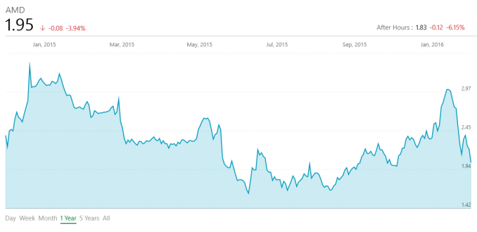
On a non-GAAP basis, AMD reports an operating loss for the quarter of $39 million, and a net loss of $79 million. For the full year 2015, the operating loss of $253 million, down from a non-GAAP operating income of $316 million in 2014. This amounts to a per share loss of $0.53 using non-GAAP numbers.AMD Q3 2015 Financial Results (GAAP) Q4'2015 Q3'2015 Q4'2014 Revenue $958M $1.06B $1.24B Gross Margin 23% 23% 29% Operating Income -$49M -$158M -$330M Net Income -$102M -$197M -$364M Earnings Per Share -$0.13 -$0.25 -$0.47
Looking at the individual segments, the Computing and Graphics segment had revenue of $470 million for the quarter, up 11% since last quarter but down 29% year-over-year. AMD had more notebook processor sales compared to last quarter, but lower client processor sales compared to last year. This segment had an operating loss of $99 million, compared to $181 million last quarter and $56 million last year. The inventory write-down last quarter was the main reason for the improvement this quarter, and lower sales caused the year-over-year drop. One good nugget for AMD is that average selling price (ASP) increase sequentially for processors, although it is down year-over-year, but GPU ASP increased both sequentially and year-over-year.AMD Q3 2015 Financial Results (Non-GAAP) Q4'2015 Q3'2015 Q4'2014 Revenue $958M $1.06B $1.24B Gross Margin 23% 23% 34% Operating Income -$39M -$97M $52M Net Income -$79M -$136M $18M Earnings Per Share -$0.10 -$0.17 $0.02
The Enterprise, Embedded, and Semi-Custom segment had revenue of $488 million, down 23% from last quarter and 15% year-over-year. Operating income was $59 million, down from $84 million last quarter and $109 million last year. AMD attributes the seasonally lower sales of semi-custom SoCs as the reason for the drop from last quarter, and the year-over-year drop is due to lower game console royalties, and lower server and embedded sales.AMD Q3 2015 Computing and Graphics Q4'2015 Q3'2015 Q4'2014 Revenue $470M $424M $662M Operating Income -$99M -$181M -$56M
The All Other segment had an operating loss of $9 million, an improvement over the $61 million loss last quarter, and a big improvement over the $383 million operating loss in Q4 2014. AMD has made some restructuring charges which affected them last quarter, and the year-over-year improvement was “primarily due to the absence of a goodwill impairment charge, lower restructuring and other special charges, net and a Q4 2014 lower of cost or market inventory adjustment.”AMD Q3 2015 Enterprise, Embedded and Semi-Custom Q4'2015 Q3'2015 Q4'2014 Revenue $488M $637M $577M Operating Income $59M $84M $109M
With a less than amazing 2015, AMD is resting a lot of hope on their new 4th generation GCN card, which they are calling Polaris. On the CPU side, they hope to execute their new Zen platform with a 40% increase in Instructions Per Clock. With AMD getting out of the fab business, they have now been relying on others to move forward on the process side, and we are finally seeing fabs other than Intel now producing FinFET based designs. Clearly AMD has a lot of work to do to not only launch the products, but execute sales of them as well. VR could also be an area where AMD could find some growth, since the requirements for VR will likely drive some GPU sales over the next 12 months.
Source: AMD Investor Relations
More...
-
01-19-16, 05:32 PM #5669
Anandtech: Intel Launches Skylake vPro With Intel Authenticate
Intel’s vPro technology has been around for quite a while now, and with every new processor generation they seem to always add more features under the vPro umbrella. For a comprehensive look at what is existing now, check out the vPro launch for Broadwell. With Skylake, Intel is trying to tackle the challenge of securing computers, and the need for complex passwords. Passwords are a big pain point in the enterprise because people don’t like to make difficult passwords, and sharing passwords can be a big problem. Social engineering and more complex attack vectors can render passwords the easiest way to get into a company’s data.
Intel is launching Intel Authenticate today, and it will require a 6th generation Intel Core processor with vPro. Authenticate will combine several factors of authentication into a single login, which, in theory, should be easier for the end user as well.
It works by combining “something you know”, which can be a PIN or password, along with “something you have”, which could be a smartphone, and “something you are”, which is biometrics. Once you include many factors, the complexity to lose all of them to the same person goes up quite a bit. The “something you know” can therefore be much easier, such as a PIN, or simple password, since that is not the defining key to the system. IT will be able to choose from multiple factors based on their own policy and preferences. Once configured, the factors are captured, encrypted, matched, and stored in hardware.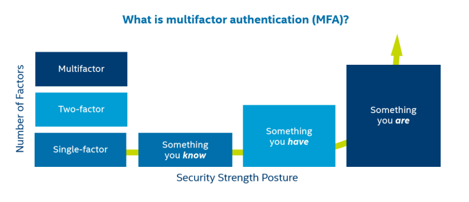
The user data never leaves the hardware, reducing the footprint for attack, and removing the chance of accidental misuse by employees. All of the authentication is then done at the hardware level once the user has matched the stored profile. The inclusion of biometrics, especially if they are based on Intel’s RealSense 3D camera systems, also adds in the possibility of having machines auto-lock when the person steps away.
Overall, this is similar to Windows Hello, except with more authentication factors and the resultant matching done on the CPU. There are advantages to this method, but one of the biggest disadvantages is that it will require Skylake class hardware and newer, so you can’t deploy it to older machines. Interestingly it is available on Windows 7, 8.1, and 10, despite Windows 7 and Skylake having a rough start together.
Intel Authenticate is available now for customers to preview.
Source: Intel
More...
-
01-20-16, 07:05 AM #5670
Anandtech: JEDEC Publishes HBM2 Specification as Samsung Begins Mass Production of Ch
The high-bandwidth memory (HBM) technology solves two key problems related to modern DRAM: it substantially increases bandwidth available to computing devices (e.g., GPUs) and reduces power consumption. The first-generation HBM has a number of limitations when it comes to capacity and clock-rates. However, the second-gen HBM promises to eliminate them.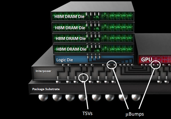
JEDEC, a major semiconductor engineering trade organization that sets standards for DRAM, recently published the final specifications of the second-generation HBM (HBM2), which means that members of the organization had ratified the standard. The new memory technology builds upon the foundation of the original JESD235 standard, which describes stacked memory devices interconnected using through silicon vias (TSVs) with a very wide input/output (I/O) interface operating at moderate data-rates. The JESD235A will help engineers to further increase performance, capacity and capabilities of HBM memory chips. HBM Gen 2 will be particularly useful for the upcoming video cards by AMD and NVIDIA, which thanks to HBM2 can feature as much as 512 GB/s – 1 TB/s of memory bandwidth and 8, 16 or even 32 GB of memory onboard.
HBM Gen 1: Good, But With Limitations
The original JESD235 standard defines the first-generation HBM (HBM1) memory chips with a 1024-bit interface and up to 1 Gb/s data-rate, which stack two, four or eight DRAM devices with two 128-bit channels per device on a base logic die. Each HBM stack (which is also called KGSD — known good stacked die) supports up to eight 128-bit channels because its physical interface is limited to 1024 bits. Every channel is essentially a 128-bit DDR interface with 2n prefetch architecture (256 bits per memory read and write access) that has its own DRAM banks (8 or 16 banks, depending on density), command and data interface, clock-rate, timings, etc. Each channel can work independently from other channels in the stack or even within one DRAM die. HBM stacks use passive silicon interposers to connect to host processors (e.g., GPUs). For more information about HBM check out our article called “AMD Dives Deep On High Bandwidth Memory — What Will HBM Bring AMD?”.
HBM gen 1 memory KGSDs produced by SK Hynix (the only company that makes them commercially) stack four 2 Gb memory dies and operate at 1 Gb/s data rate per pin. AMD uses these KGSDs with 1 GB capacity and 128 GB/s peak bandwidth per stack to build its Fiji GPU system-in-packages (SiPs) and the Radeon R9 Fury/R9 Nano video cards. The graphics adapters have 4 GB of VRAM onboard, not a lot for 2016. While AMD’s flagship video cards do not seem to have capacity issues right now, 4 GB of memory per graphics adapter is a limitation. AMD’s latest graphics cards sport 512 GB/s of memory bandwidth, a massive amount by today’s standards, but even that amount could be a constraint for future high-end GPUs.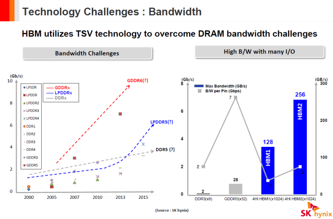
HBM Gen 2: Good Thing Gets Better
The second-generation HBM (HBM2) technology, which is outlined by the JESD235A standard, inherits physical 128-bit DDR interface with 2n prefetch architecture, internal organization, 1024-bit input/output, 1.2 V I/O and core voltages as well as all the crucial parts of the original tech. Just like the predecessor, HBM2 supports two, four or eight DRAM devices on a base logic die (2Hi, 4Hi, 8Hi stacks) per KGSD. HBM Gen 2 expands capacity of DRAM devices within a stack to 8 Gb and increases supported data-rates up to 1.6 Gb/s or even to 2 Gb/s per pin. In addition, the new technology brings an important improvement to maximize actual bandwidth.
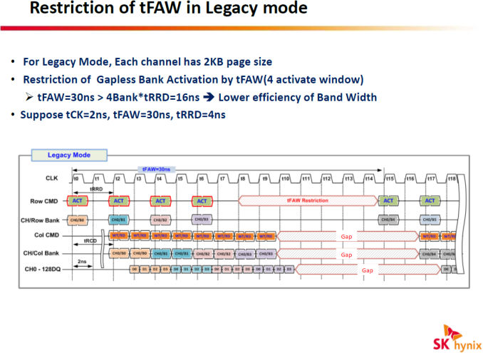
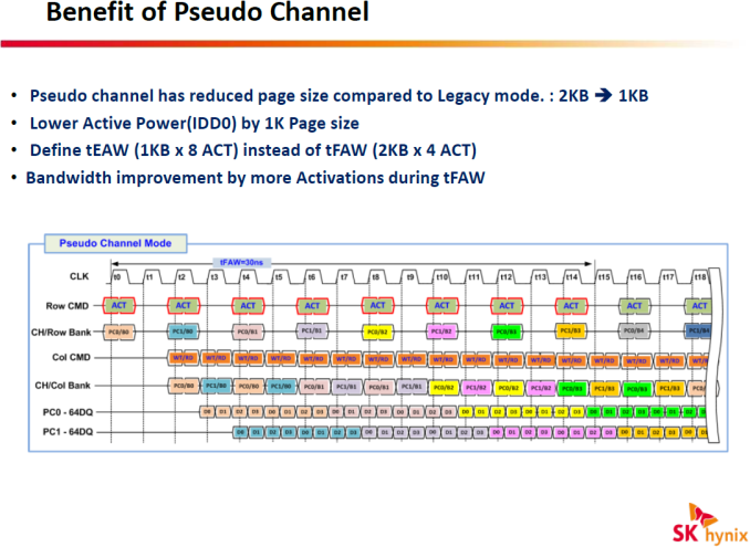
One of the key enhancements of HBM2 is its Pseudo Channel mode, which divides a channel into two individual sub-channels of 64 bit I/O each, providing 128-bit prefetch per memory read and write access for each one. Pseudo channels operate at the same clock-rate, they share row and column command bus as well as CK and CKE inputs. However, they have separated banks, they decode and execute commands individually. SK Hynix says that the Pseudo Channel mode optimizes memory accesses and lowers latency, which results in higher effective bandwidth.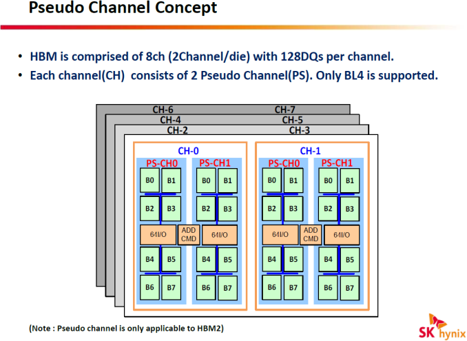
If, for some reason, an ASIC developer believes that Pseudo Channel mode is not optimal for their product, then HBM2 chips can also work in Legacy mode. While memory makers expect HBM2 to deliver higher effective bandwidth than predecessors, it depends on developers of memory controllers how efficient next-generation memory sub-systems will be. In any case, we will need to test actual hardware before we can confirm that HBM2 is better than HBM1 at the same clock-rate.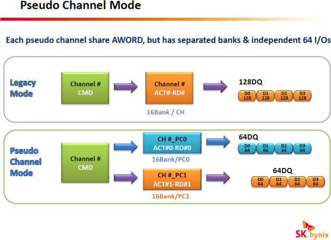
Additional improvements of HBM2 over the first-gen HBM includes lane remapping modes for hard and soft repair of lanes (HBM1 supports various DRAM cell test and repair techniques to improve yields of stacks, but not lane remapping), anti-overheating protection (KGSD can alert memory controllers of unsafe temperatures) and some other.
The second-generation HBM memory will be produced using newer manufacturing technologies than the first-gen HBM. For example, SK Hynix uses its 29nm process to make DRAM dies for its HBM1 stacks. For HBM2 memory, the company intends to use their 21nm process. Thanks to newer manufacturing technologies and higher effective bandwidth, HBM2 should have higher energy efficiency than HBM1 at its data-rates, but we do not have exact details at this point. In any case, HBM2 is likely to be more energy efficient than GDDR5 and GDDR5X, hence the odds are good that it will be the memory of choice for high-end graphics cards in the future.
Samsung Electronics this week said that it had begun mass production of HBM2 memory, but did not reveal too many details. Samsung's HBM2 KGSD features 4 GB capacity, 2 Gb/s data rate per pin and is based on four 8 Gb DRAM dies. The memory chips will let device manufacturers build SiPs with up to 16 GB of memory. It is noteworthy that Samsung decided to use 8 Gb DRAM dies for its HBM2 stacks. Such decision looks quite logical since with 8 Gb DRAM ICs the company can relatively easily increase or decrease capacity of its KGSDs by altering the number of DRAM layers. The DRAM maker uses its 20nm process to produce its HBM2 DRAM KGSDs. Unfortunately, Samsung did not reveal actual power consumption of the new memory stacks.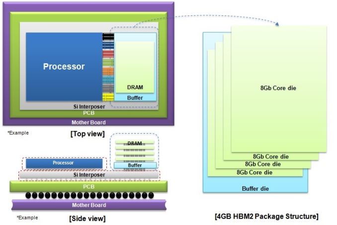
Larger PackageGPU Memory Math AMD Radeon R9 290X NVIDIA GeForce GTX Titan X AMD Radeon R9 Fury X Samsung's 4-Stack HBM2 based on 8 Gb DRAMs Theoretical GDDR5X 256-bit sub-system Total Capacity 4 GB 12 GB 4 GB 16 GB 8 GB Bandwidth Per Pin 5 Gb/s 7 Gb/s 1 Gb/s 2 Gb/s 10 Gb/s Number of Chips/Stacks 16 24 4 4 8 Bandwidth Per Chip/Stack 20 GB/s 14 GB/s 128 GB/s 256 GB/s 40 GB/s Effective Bus Width 512-bit 384-bit 4096-bit 4096-bit 256-bit Total Bandwidth 320 GB/s 336 GB/s 512 GB/s 1 TB/s 320 GB/s Estimated DRAM
Power Consumption30W 31.5W 14.6W n/a 20W
HBM2 memory stacks are not only faster and more capacious than HBM1 KGSDs, but they are also larger. SK Hynix’s HBM1 package has dimensions of 5.48 mm × 7.29 mm (39.94 mm2). The company’s HBM2 chip will have dimensions of 7.75 mm × 11.87 mm (91.99 mm2). Besides, HBM2 stacks will also be higher (0.695 mm/0.72 mm/0.745 mm vs. 0.49 mm) than HBM1 KGSDs, which may require developers of ASICs (e.g., GPUs) to install a heat-spreader on their SiPs to compensate for any differences in height between the memory stacks and GPU die, to protect the DRAM, and to guarantee sufficient cooling for high bandwidth memory.
Larger footprint of the second-gen HBM2 means that the upcoming SiPs with multiple memory stacks will require larger silicon interposers, which means that they are going to be slightly more expensive than SiPs based on the first-gen HBM. Since geometric parameters of staggered microbump pattern of HBM1 and HBM2 are the same, complexity of passive silicon interposers will remain the same for both types of memory. A good news is that to enable 512 GB/s of bandwidth, only two HBM2 stacks are needed, which implies that from bandwidth per mm2 point of view the new memory tech continues to be very efficient.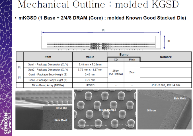
Since SK Hynix’s HBM1 KGSDs are smaller than the company’s HBM2 stacks, they are going to have an advantage over the second-gen high-bandwidth memory for small form-factor SiPs. As a result, the South Korea-based DRAM maker may retain production of its HBM1 chips for some time.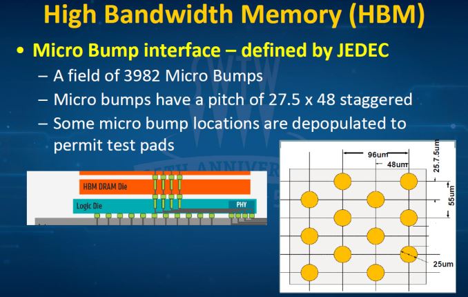
A slide by FormFactor and Teradyne from their presentation at Semiconductor Wafer Test Workshop 2015
New Use Cases and Industry Support
Thanks to higher capacity and data-rates, HBM2 memory stacks will be pretty flexible when it comes to configurations. For example, it will be possible to build a 2 GB KGSD with 256 GB/s of bandwidth that will use only two 8 Gb memory dies. Such memory stack could be used for graphics adapters designed for notebooks or ultra-small personal computers. Besides, it could be used as an external cache for a hybrid microprocessor with built-in graphics (in the same manner as Intel uses its eDRAM cache to boost performance of its integrated graphics processors). What remains to be seen is the cost of HBM2 stacks that deliver 256 GB/s bandwidth. If HBM2 and the necessary interposer remains as expensive as HBM1, it will likely continue to only be used for premium solutions.
Thanks to a variety of KGSD configurations prepared by DRAM manufacturers, expect new types of devices to start using HBM2. Samsung and SK Hynix believe that in addition to graphics and HPC (high-performance computing) cards, various server, networking and other applications will utilize the new type of memory. As of September, 2015, more than 10 companies were developing system-on-chips (including ASICs, x86 processors, ASSPs and FPGAs) with HBM support, according to SK Hynix.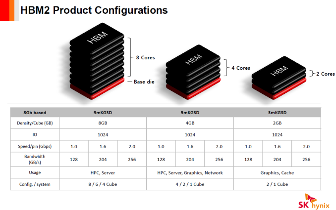
The first-generation HBM memory delivers great bandwidth and energy efficiency, but it is produced by only one maker of DRAM and is not widely supported by developers of various ASICs. By contrast, Samsung Electronics and SK Hynix, two companies that control well over 50% of the global DRAM output, will make HBM2. Micron Technology yet has to confirm its plans to build HBM2, but since this is an industry-standard type of memory, the door is open if the company wishes to produce it.
Overall, the industry support for the high bandwidth memory technology is growing. There are 10 companies working on SoCs with HBM support, leading DRAM makers are gearing up to produce HBM2. The potential of the second-gen HBM seems to be rather high, but the costs remain a major concern. Regardless, it will be extremely interesting to see next-generation graphics cards from AMD and NVIDIA featuring HBM2 DRAM and find out what they are capable of because of the new Polaris and Pascal architectures as well as the new type of memory.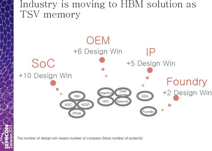
More...


 Quote
Quote
Thread Information
Users Browsing this Thread
There are currently 8 users browsing this thread. (0 members and 8 guests)


Bookmarks