

Results 5,711 to 5,720 of 12095
Thread: Anandtech News
-
02-09-16, 04:16 AM #5711
Anandtech: CEO of Imagination Technologies Steps Down
Sir Hossein Yassaie, chief executive officer of Imagination Technologies, has stepped down as of Monday, Feburary 8th. Mr. Yassaie served as Imagination’s CEO since 1998 and joined the company in 1992. The company expects to report a loss for the financial year, which may be the reason for CEO’s departure. Andrew Heath, one of the company's non-executive directors, has been appointed interim chief executive. He has already began to search for a new CEO for Imagination.
Imagination licenses graphics, multimedia and general-purpose processing technologies to various chip developers, including Apple and Intel. The company indicated that royalties from some of its key customers have fallen short of previous expectations for the last calendar quarter of 2015. The company also lowered its forecast for Q1 2016. Imagination named global slowdown in the semiconductor sector as well as global uncertainty about future trading prospects with China as the reasons for its financial problems. While Imagination indicated that its licensing pipeline remains strong, it is not sure about its license revenue timing.
Imagination Technologies was founded in 1985 as VideoLogic. The company sold chips for televisions, game consoles and PCs. Mr. Yassaie changed the company’s business model to technology licensing in 1999 and essentially exited chip business several years later. Imagination tried to return to the market of graphics adapters with its Kyro and Kyro II graphics chips in early 2000s, but it could not compete against ATI and NVIDIA at the time. Starting from the year 2000 Imagination bought a number of important technology companies, significantly boosting its IP portfolio. Among the companies acquired by Imagination are Ensigma (digital signal processing), Caustic Graphics (hardware/software for real-time ray-tracing technology), MIPS Technologies (general-purpose processing) and a number of others. Today, Imagination can provide virtually all technologies needed to build system-on-chips for almost all kinds of devices. In fact, Imagination’s graphics processing technologies are used inside billions of smartphones and tablets.
Imagination did not announce when it expects to hire its new CEO, but said that it will consider both internal and external candidates. For a company like Imagination the absence of permanent CEO concerning because it constantly needs to make strategic decisions that have long-lasting effects on its future. Technologies developed by Imagination today will be licensed only a couple of years down the road and it is important for them to be competitive against offerings from ARM as well as developers of proprietary chips. As pointed out by The Tech Report, Mr. Yassaie is the author of the intellectual property licensing model that brought the company to fame, and it will likely not be easy to find a replacement due to the complexity of the technology licensing business.
Alongside Mr. Yassaie's resignation, Imagination also announced additional details on restructuring initiatives, which include the sale of Pure, its consumer electronics business. The company expects to reduce operating costs of its on-going businesses by £15 million in the next financial year, ending April 2017. In addition, Imagination will re-invest £2 million in PowerVR graphics processing technology. The company also plans to analyze its overhead expenses and research and development expenditures before implementing additional restructuring actions.
More...
-
02-09-16, 11:06 AM #5712
Anandtech: Micron Reports on GDDR5X Dev Progress - Volume Production This Summer
Engineers from Micron Development Center in Munich (also known as Graphics DRAM Design Center) are well known around the industry for their contribution to development of multiple graphics memory standards, including GDDR4 and GDDR5. The engineers from MDC also played a key role in development of GDDR5X memory, which is expected to be used on some of the upcoming video cards. Micron disclosed the first details about GDDR5X in September last year, publicizing the existance of the standard ahead of later JEDEC ratification and offering a brief summary of what to expect. Since then the company has been quiet on their progress with GDDR5X, but in a new blog post they have published this week, the company is touting their results with their first samples and offering an outline of when they expect to go into volume production.
The GDDR5X standard, as you might recall, is largely based on the GDDR5 technology, but it features three important improvements: considerably higher data-rates (up to 14 Gbps per pin or potentially even higher), substantially higher-capacities (up to 16 Gb), and improved energy-efficiency (bandwidth per watt) thanks to 1.35V supply and I/O voltages. To increase performance, the GDDR5X technology uses its new quad data rate (QDR) data signaling technology to increase the amount of data transferred, in turn allowing it to use a wider 16n prefetch architecture, which enables up to 512 bit (64 Bytes) per array read or write access. Consequently, GDDR5X promises to double the performance of GDDR5 while consuming similar amounts of power, which is a very ambitious goal.
In their blog post, Micron is reporting that they already have their first samples back from their fab - this being earlier than expected - with these samples operating at data-rates higher than 13 Gbps in the lab. At present, the company is in the middle of testing its GDDR5X production line and will be sending samples to its partners this spring.
Thanks to reduction of Vdd/Vddq by 10% as well as new features, such as per-bank self refresh, hibernate self refresh, partial array self refresh and other, Micron’s 13 Gbps GDDR5X chips do not consume more energy than GDDR5 ICs (integrated circuits) — 2–2.5W per component (i.e., 10–30W per graphics card), just like the company promised several weeks ago. Since not all applications need maximum bandwidth, in certain cases usage of GDDR5X instead of its predecessor will help to reduce power consumption.
GDDR5X memory chips will come in new packages, which will be slightly smaller (14×10mm vs. 14×12mm) compared to GDDR5 ICs despite the increase of their ball count (190-ball BGA vs. 170-ball BGA). According to Micron, denser ball placement, reduced ball diameter (0.4mm vs. 0.47mm) and smaller ball pitch (0.65mm vs. 0.8mm) make PCB traces slightly shorter, which should ultimately improve electrical performance and system signal integrity. Keeping in mind higher data-rates of GDDR5X’s interface, improved signal integrity is just what the doctor ordered. The GDDR5X package maintains the same 1.1mm height as the predecessor.
Micron is using its 20 nm memory manufacturing process to make the first-generation 8 Gb GDDR5X chips. The company has been using the technology to make commercial DRAM products for several quarters now. As the company refines its fabrication process and design of the ICs, their yields and data-rate potential will increase. Micron remains optimistic about hitting 16 Gbps data-rates with its GDDR5X chips eventually, but does not disclose when it expects that to happen.
All of that said, at this time the company has not yet figured out its GDDR5X product lineup, and nobody knows for sure whether commercial chips will hit 14 Gbps this year with the first-generation GDDR5X controllers. Typically, early adopters of new memory technologies tend to be rather conservative. For example, AMD’s Radeon HD 4870 (the world’s first video card to use GDDR5) was equipped with 512 MB of memory featuring 3.6 Gbps data-rate, whereas Qimonda (the company which established Micron’s Graphics DRAM Design Center) offered chips with 4.5 Gbps data-rate at the time.
The first-gen GDDR5X memory chips from Micron have 8 Gb capacity, hence, they will cost more than 4 Gb chips used on graphics cards today. Moreover, due to increased pin-count, implementation cost of GDDR5X could be a little higher compared to that of GDDR5 (i.e., PCBs will get more complex and more expensive). That said, we don't expect to see GDDR5X showing up in value cards right away, as this is a high-performance technology and will have a roll-out similar to GDDR5. At the higher-end however, a video card featuring a 256-bit memory bus would be able to boast with 8 GB of memory and 352 GB/s of bandwidth.
Finally, Micron has also announced in their blog post that they intend to commence high-volume production of GDDR5X chips in mid-2016, or sometime in the summer. It is unknown precisely when the first graphics cards featuring the new type of memory are set to hit the market, but given the timing it looks like this will happen in 2016.
More...
-
02-09-16, 01:49 PM #5713
Anandtech: Skylake Overclocking: Regular CPU BCLK Overclocking is Being Removed
If you follow PC technology news, you would have seen our news on how Supermicro had enabled overclocking for Skylake (Intel’s 6th Generation) processors on non Z170 motherboards. This was a two fold increase in interest – not only was there overclocking (via base frequency rather than multiplier) on an H series chipset more than a few MHz, but it also enabled this type of overclocking on locked processors from $60 and up.
We reported at the time that ASRock was also introducing this feature, and since then they promoted a new series of ‘Sky OC’ features to enable base frequency overclocking on locked (often called ‘non-K’ because these chips do not have the K letter in their name to denote overclocking) processors. At CES we were shown new motherboards that were not Z170 motherboards that also had the vital feature – the extra signal generator required for the processor to enable this and a variant of custom firmware. Other motherboard manufacturers were also interested in pursuing this line, although they were a little more reserved.
Core i3-6300T overclocked by 20%
Since that news we have sourced both the Supermicro motherboard that started the trend as well as more mid-range Core i3 processor for a review. Testing is almost complete, but there is a new climax to this story.
In the past week or so, it turns out that this feature is being removed for non-overclocking focused CPUs. The most obvious indication that this feature is no-longer part of the ecosystem comes from ASRock – their BIOS updates lists new firmware for all of their models which have the feature removed with the following phrase:
The marketing for this feature has all been removed as well, from ASRock’s websites and adverting.
When we (and other media) spoke to the other motherboard manufacturers, noting how reserved they were at the time this ‘feature’ came to prominence; we were told that it was still a work in progress for them. Some were uneasy to guarantee stability, or were not in a position to issue direct updates as some of their products did not have the required hardware and it would have left a confusing product stack with some having the feature and others not. As a result we expected to see new motherboards with the feature over time, either ‘revision/mark 2’ variants or a hold out for the Kaby Lake platform later this year and introduce it there.
Since ASRock were removing the feature, there have been plenty of comments abound on forums as to the reason behind this. The removal of the feature also comes with a CPU microcode update, which is notable because it could mean that both updates are linked. Most are pointing the finger at Intel, wondering if they are flexing some muscle requiring the manufacturer to change the firmware, or it's being done via microcode, while some are blaming the media for featuring it as a big wow factor and bringing it into the radar more prominently. I want to address some of these points and a wider look at Intel’s strategy here.
Firstly, no matter which way you slice it, Intel has been actively promoting overclocking as a big feature of their processors. It was a big part of the Skylake launch back in August last year.
To put some history in here, overclocking the processor by the the base frequency was common place with Conroe, and then with Nehalem there were special SKUs that opened up the multiplier. With Sandy Bridge, the microarchitecture was designed very differently and more parts of the silicon were integrated into the same clock domain which restricted any base frequency overclocking quite severely. Intel also restricted overclocking via the multiplier to a couple of parts with K in the name (typically high end i5 and i7 parts) such that overclocking could be focused on the high margin processors. This meant that users had to focus on getting more out of the better silicon, rather than pushing a mid-range part into a better performance chip. Some may argue this was to increase high end processor sales, while others saw it as Intel having a performance lead and being able to structure their product stack in such a way to maximize that lead.
In July 2014, with Devil’s Canyon, Intel adjusted the beams slightly. Partly due to an increase in temperature generation with the integrated voltage regulator on Haswell and a decrease in thermal interface quality, Devil’s Canyon was released offering more thermal headroom and potentially better overclocking performance – we tested the i7-4790K and i5-4690K and came to this conclusion. Alongside the two Devil’s Canyon processors they also released an overclockable Pentium processor, the G3258, to mark the 20th anniversary of Pentium. This was a dual core part without hyperthreading which offered a 30-40% overclock, but as we found out in the review of the G3258, even with this OC the fact that it was dual core limited its usefulness in a word were software/gaming is designed to handle more than two threads. At the time, for most enthusiasts, it was clear that if Intel wanted to relaunch the mid-range market, then an unlocked Core i3 needed to be made. It has been clear that while Intel holds the competitive advantage, that was not on the cards – releasing an unlocked Core i3 would give users performance of an i5/i7 at a much lower price point, and would cannibalize sales of their high end parts. While they had no competition for raw CPU horsepower, it wasn’t going to happen, regardless of how heavily Intel was promoting overclocking and how good overclocked processors were for gaming.
Fast forward to Skylake, and the first processors released were the two overclocked chips – the i7-6600K and i5-6500K, which we reviewed on day one. These were released at Gamescom in August 2015, a primarily gaming focused event and were marketed as unlocked parts ideal for gaming. These processors were arguably as rare as hen’s teeth to find until September. It was more at IDF, a couple of weeks later, that we given that the architectural details of the new CPUs and allowed us to explain why we were seeing the performance numbers we did. The reason why they were released at Gamescom was simply for the gaming crowd, as gaming is one of the few growth markets in the PC industry, but it meant that the overclocking discussions happened later at IDF. Intel invited experienced overclockers on stage during the presentations to show off overclocking on the new parts – it was clear that overclocking is on the agenda. We found out at IDF that the new Skylake microarchitecture uses separate frequency domains for the IO and PCIe, allowing the base frequency of these new unlocked parts to be adjusted as well as the multiplier.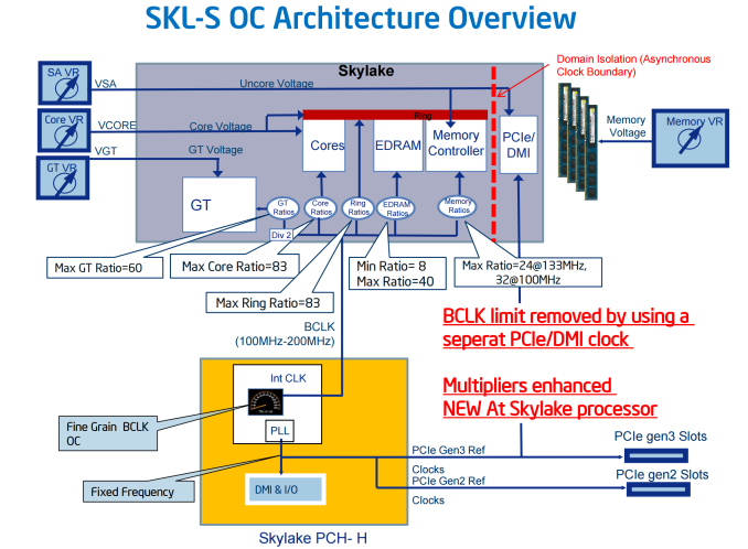
In September 2015, the other members of the Skylake family were released: the 65W parts, the lower power parts, the Core i3 and the Pentium processors. Despite what was being said about being committed to overclocking as a concept/feature, these parts as we expected were locked down in terms of multiplier, but surprisingly locked down in base frequency as well. We had a chance to test some 65W parts, but were only able to move 3% or so, and this was a hard wall rather than a decline.
Splave and L0ud_sil3nc3 at IDF 2015 overclocking live with Intel's Kirk Skaugen (source)
Brian Krzanich, CEO of Intel, with Splave, L0ud_sil3nc3 and Fugger during IDF 2015(source)
So again, move forward to November 2015, when we wrote about Supermicro working around this 3% limitation using an external clock generator and modified firmware. It essentially opened the floodgates – not only could you overclock by adjusting the base frequency on a non Z-series chipset, but also on processors that were previously locked or only moved 3%. There was still the limitation of the DRAM increasing in frequency, but it was good enough for enthusiasts to start asking about the motherboard and other motherboard manufacturers to do something similar. Very quickly we were speaking to all the major players about their plans, with ASRock leading the way in that regard. They were quick enough to roll out the new feature on motherboards that could support it, and were taking motherboards already on the design stage up a notch to support it. We tested the i3-6100TE and got to 140 MHz very easily without any voltage increases, giving a 40% overclock.
Core i3-6320 overclocked to 127 MHz on a Supermicro C7H170-M
So in this past week, ASRock has rolled back this feature on the latest BIOS updates. I am in contact with Supermicro as to their perspective on all this. Because of the scale of the rollback and how sudden it was, it is understandable that many users are pointing the finger at Intel, and wondering if there is some muscle being flexed to make this rollback occur. There is obvious finger pointing – if motherboard manufacturers had this feature, and a overclocked Core i3 performed as well as a Core i5-6600K in games, then users might spend $100 less on the processor. Not only end users, but system integrators as well would take advantage of this, offering cheaper pre-overclocked systems that gave higher performance. It would mean that users would upgrade today and keep their system longer, which might be contrary to any strategy for reinvigorating the PC market. Not only the CPU, but saving money on chipsets by buying H or B series would also affect the bottom line.
If you believe that Intel is worth pointing the finger at here, there are plenty of signs that show the two conflicting sides of interest – while promoting overclocking as a major part of the platform on one hand, not allowing overclocking on the low end SKUs with the other seems at odds with the overclocking strategy. There is something to be said about controlling the user experience, making sure the user gets what they paid for rather than a burning pile of rubble due to misconfiguration, or we could look to the fact that if base frequency overclocking is occurring now, then it would invariably end up with Kaby Lake as well. Depending on how Kaby Lake turns out, this might (or might not) be a good (or bad) thing for Intel.
Of course, there could be a few dangers given it was enabled mid-cycle. Allowing overclocking on an H-series or B-series chipset might not be a good thing, especially if the motherboard is only designed for 65W parts from a power delivery perspective. If the CPU is designed for 35W/65W and starts to draw 120W+ or 200W+, with a motherboard that was only expecting 65W, then it would not last very long. That would mean some motherboards would have to be engineered to do so, but as mentioned before, having a blanket upgrade regardless of the motherboard design would leave the company product stack with some parts that could and others that couldn’t, potentially confusing end-users.
Also of potential concern/confusion here are warranty matters for overzealous overclocks. As part of their overclocking strategy Intel does in fact offer overclocking warranties in some regions via their optinal 'Performance Tuning Protection' plans, but again this is only for SKUs that are unlocked. With lower-end processors I think it's safe to say that Intel doesn't want to open the door again to replacing lower-margin processors that died under "mysterious circumstances" while trying to balance that with legitimate consumer warranty needs.
Arguably the best way to encourage these CPUs to be opened up is some strong competition. It's at this point that I should add that despite the opening up of the clock domains with Skylake, Intel has been clear in talking about their overclock strategy only in relation to the unlocked parts. This makes sense given their market position.
Back on the motherboard side, assuming that Supermicro will also have to roll back their feature (or limit it to that single motherboard only, which might be difficult to get hold of), then there are two options here for anyone who had invested in the base frequency ecosystem. Either stay on the older BIOS and not update as time goes on, or update and lose the feature. We’re not sure if ASRock will keep the BIOSes that allow base frequency on their website, or if they will be removed so new users cannot roll back the BIOS. I assume that some forums have taken a copy while they were all still available and hosted them elsewhere, such as the overclocking forum HWBot or at XtremeSystems.
Not to mention, there's the consideration for reviewers as well. For those that have an OC capable system for these locked parts, creating data at an overclocked speed and base speed means double the time to test, although there will be fewer users able to buy the hardware necessary to do so as time goes on. From a personal perspective, I still want to see those OC numbers on Core i3 or Pentiums, or even the Core i5-6400/6500 where a user could have saved $60 compared to the i5-6600K, or comparing that to what the competitors have to offer. How OC makes a difference allows us to predict performance. I assume our readers want to see as well?
Relevant Reading
Devil's Canyon Review: Core i7-4790K and Core i5-4690K - CPU Review
The Overclockable Pentium G3258 Review - CPU Review
Skylake-K Review: Core i7-6700K and Core i5-6600K - CPU Review
Comparison between the i7-6700K and i7-2600K in Bench - CPU Comparison
Overclocking Performance Mini-Test to 4.8 GHz - Overclocking
Skylake Architecture Analysis - Architecture
Z170 Chipset Analysis and 55+ Motherboards at Launch - Motherboard Overview
Discrete Graphics: An Update for Z170 Motherboards - PCIe Firmware Update
More...
-
02-10-16, 08:06 AM #5714
Anandtech: Plextor Introduces M6S Plus SSDs with Toshibas 15nm MLC NAND
Plextor this week introduced its M6S Plus SSDs that use Toshiba’s latest MLC NAND flash memory as well as a proven controller from Marvell. The new SSDs offer the same level of performance and the same feature set as their predecessors, the M6S drives introduced in 2014. The drives offer read and write speeds expected from SATA SSDs as well as Plextor’s technologies designed to guarantee high reliability and high performance after long periods of usage.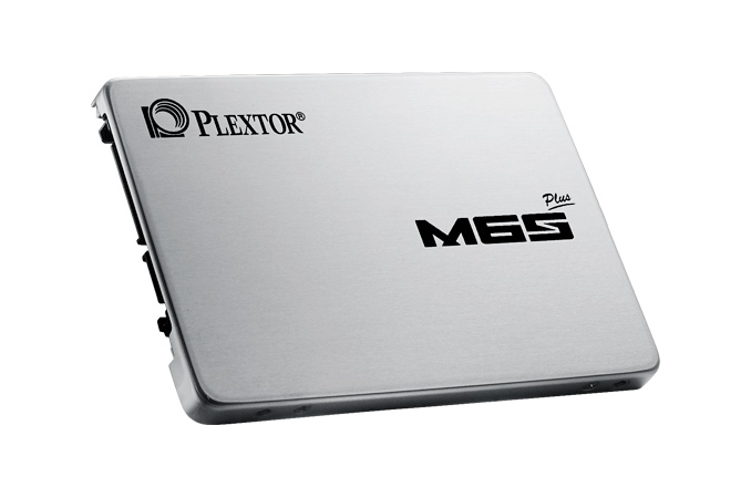
The new Plextor M6S Plus SSDs are based on the Marvell 88SS9188 controller as well as Toshiba’s newest 15 nm MLC NAND. Earlier Plextor offered M6S solid-state drives based on the same controller chip, but featured Toshiba’s older 19 nm MLC NAND. Apparently, Plextor will have to switch to a new type of NAND as manufacturers tend to decrease production of memory using outdated process technologies. The new drives are offered in 2.5-inch/7 mm form-factor and use the SATA-6 Gb/s interface.
The Plextor M6S Plus SSDs feature 128 GB, 256 GB and 512 GB capacities. They are rated to offer maximum sequential read/write speed of up to 520/440MB/s. Maximum random 4K read/write speed declared by Plextor is 94K/80K IOPS (input/output operations per second). It is noteworthy that to guarantee high performance, the new SSDs from Plextor are equipped with up to 768 MB of DDR3 DRAM-based cache.
Notably, the performance specifications for the new M6S Plus lineup is identical to that of the previous M6S series. As Plextor didn't switch controllers and didn't switch NAND vendors, this means that they most likely are just using 15nm NAND as a drop-in replacement for their existing designs, and there won’t be any generational performance changes such as using fewer, higher capacity NAND dies. This has been an issue in the past when vendors have switched to newer generation NAND and labeled the resulting product under an old brand, so kudos to Plextor for making the 15nm drives their own line anyhow.Specifications of Plextor M6S Plus SSDs PX-128M6S+ PX-256M6S+ PX-512M6S+ Capacity 128 GB 256 GB 512 GB Controller Marvell 88SS9188 NAND Toshiba, MLC 15nm Cache 256 MB DDR3 512 MB DDR3 768 MB DDR3 Sequential Read Speed up to 520 MB/s up to 520 MB/s up to 520 MB/s Sequential Write Speed up to 300 MB/s up to 420 MB/s up to 440 MB/s 4K Random Read up to 88K IOPS up to 90K IOPS up to 94K IOPS 4K Random Write up to 75K IOPS up to 80K IOPS up to 80K IOPS Form-Factor 2.5-inch/7mm Interface SATA-6 Gbps
However while the switch to 15nm NAND doesn't impact performance, it's unclear whether the endurance of the newer M6S Plus series has been impacted, as the company hasn't published any endurance figures for the new drives. Typically, MLC NAND produced using thinner fabrication process has lower P/E cycle rating compared to flash memory produced using thicker manufacturing technology. The 19nm M6S series was rated for 72TB, so it will be interesting to see where the M6S Plus ends up.
Moving on, contemporary Plextor’s SSDs also ship with the company’s PlexTurbo RAM caching technology, which is aimed to improve performance beyond limitations of SATA-6Gb/s interface. The caching works like RAM disk, hence, uses system memory. The M6S Plus also supports TrueSpeed (supposed to guarantee maximum performance over long usage periods) and TrueProtect (a multi-layer error correction capability) firmware-based technologies developed by the company.
Finally, though the exact MSRPs of the Plextor M6S Plus drives haven't been published, Amazon has started to list the drives at their store. Amazon currently lists the 128 GB version for $62, the 256 GB model for $91, and the 512 GB flavor for $166. As this is a higher tier drive these prices put it above the increasingly large number of TLC drives on the market, but not immensely so. At the same time if performance is indeed similar to the original M6S, it should handily outperform these drives in most situations. Apparently, the recent price drops of NAND flash helped Plextor to build inexpensive SSDs based on 15 nm MLC NAND flash from Toshiba, which given the race to the bottom in the TLC market is not a bad choice for Plextor.
More...
-
02-11-16, 07:15 AM #5715
Anandtech: The Lenovo Ideapad Y700 Laptop Review
The PC gaming market has been pretty strong market over the last couple of years, and recent developments have pushed the boundaries again. With launches of virtual reality headsets, we’ve seen even notebook manufacturers getting prepared to drive these new devices, but it takes a lot of compute to do it. Manufacturers going after sales of gaming notebooks are going to be able to eke out better margins too, so it’s an area many of them focus on. But the typical gaming notebook is going to be quite expensive. A powerful mobile GPU, nice display, and good processor, are all going to add to the bill of materials. For those that want to get into the market for a gaming notebook, sometimes you don’t want to break the bank.
More...
-
02-11-16, 08:51 AM #5716
Anandtech: EVGA Begins Selling "VR Edition" GeForce GTX Video Cards for VR Gaming Rig
EVGA this week began to sell their GeForce GTX 980 Ti VR Edition video cards, a new lineup tailored for those who plan to use a virtual reality headset. The graphics boards are equipped with an internal HDMI port and a special adapter for 5.25-inch bay that simplifies plugging VR headsets to PCs.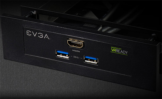
The family of EVGA’s VR Edition graphics cards currently includes two models, both of which are modifications of EVGA's existing GTX 980 Ti card designs. The first VR Edition card is the EVGA GeForce GTX 980 Ti VR Edition Gaming ACX 2.0+ (06G-P4-3996), which uses the company’s own ACX 2.0+ cooler featuring 8-mm copper heatpipes, aluminum radiators, two fans and a memory/MOSFET cooling plate, while the second is the EVGA GeForce GTX 980 Ti VR Edition Gaming (06G-P4-3998), which uses NVIDIA’s reference cooler for high-end boards. As these are GTX 980 Ti cards, both cards are based on the GM200 GPU with 2816 stream processors, 176 texture units, 96 ROPs as well as a 384-bit memory bus. The GPUs are clocked at 1000 MHz/1076 MHz (base/boost), whereas the attaced 6 GB of GDDR5 memory is clocked at 7 Gbps.
A brief examination of the pictures provided on EVGA's website indicates that both VR Edition graphics cards are using PCBs that resemble NVIDIA’s reference designs for the GeForce GTX 980 Ti/Titan X (8pin + 6pin power inputs), but they feature an important addition. The adapters have an internal HDMI 2.0 port that connects to a special adapter for 5.25-inch bay that has an HDMI output as well as two USB 3.0 connectors. The adapter is designed to connect the Oculus Rift, the HTC Vive or any other VR headset to a PC without using ports on the backside of the computer, which makes the process considerably more comfortable.
EVGA's product literature indicates that they're primarily focused on first-time buyers - those who will be building or upgrading systems ahead of the spring VR headset launches - as these headsets will be launching some time before any 16nm high-end GPUs. That said, I wouldn't be surprised if the VR Edition cards also proved popular with gamers who already have a PC powered by the GeForce GTX 980 Ti and are looking forward to build a multi-GPU system to play VR games, as VR SLI scaling is looking optimisitc thanks to the ability to forgo AFR and assign a GPU to each eye.
From a design perspective, routing HDMI port to the backside of the card should be relatively easy. EVGA hasn't released any board shots, but they likely only had to slightly modify voltage regulating module of their GeForce GTX 980 Ti boards without any significant changes to its design. Consequently I wouldn't be surrprised if other makers of video cards do something similar later on - the idea seems rather obvious in hindsight - though for the moment EVGA is the first and only game in town. Perhaps, if VR gaming takes off in the next year or two, AMD and NVIDIA could add internal graphics ports to their reference designs.
Both EVGA GeForce GTX 980 Ti VR Edition graphics cards are available now for $699, which comes at around a $70 premium over their normal reference-clocked GeForce GTX 980 Ti boards (usually $620 - $630). As it appears, VR gamers will have to pay a extra for the VR adapter for 5.25” bays. However, given the additional comfort, it may well worth the investment, especially for those who plan on frequently plugging and unplugging VR headsets (or for that matter even tradtional HDMI displays).
Gallery: EVGA Starts to Sell GeForce GTX Video Cards for VR Gaming Rigs


More...
-
02-11-16, 09:35 AM #5717
Anandtech: Qualcomm Announces Snapdragon 625, 425 & 435 Mid- and Low-End SoCs
Today Qualcomm announces three new SoCs in the mid- and low-end Snapdragon lineup. At the lowest end we find the Snapdragon 425 offering a very frugal CPU configuration consisting of 4x Cortex A53's clocked in at 1.4GHz. The chipset is aimed at replacing the Snapdragon 410 and 412 and improves on them with an upgrade on the modem block as well as media decoder and encoder capabilities, now enabling 1080p HEVC decode and encode.
The Snapdragon 435 replaces the Snapdragon 430 which was only announced just a few months ago and also sees an improvement in the modem block used as we see it now going from UE Category 4 to UE Category 7. On the CPU side we see a 200MHz boost in the frequency of the faster of the two quad-core A53 clusters, now reaching 1.4GHz. In both the Snapdragon 425 and 435 we don't see a change in the GPU but it's possible clocks have changed; Unfortunately details on the matter are still sparse. Both the Snapdragon 425 and 435 are manufactured on a "28nm LP" process but sadly it wasn't specified which foundry is manufacturing them.
Most importantly comes the announcement of the Snapdragon 625. This is the successor to the Snapdragon 617 which along with the 615 has seen quite a lot of success in mid-range and budget smartphones. The CPUs remain two quad-core clusters of Cortex A53's but now the performance cluster is clocked at up to 2GHz representing a large increase to the 1.5GHz SoCs which the 625 is replacing. The GPU has also been upgraded from an Adreno 405 to a newer generation Adreno 506. The modem again has seen a slight upgrade from an X8 to an X9 block, allowing for an increase in the uplink performance if the network supports it.New 2016 Mid- to Low-End Snadpragons SoC Snapdragon 425
(MSM8917)Snapdragon 435
(MSM8940)Snapdragon 625
(MSM8953)CPU 4x A53 @ 1.4GHz4x A53 @ 1.4GHz
4x A53 @ ? GHz4x A53 @ 2.0GHz
4x A53 @ ? GHzMemory 1x 32-bit @ 800MHzLPDDR3
5.3GB/s b/w1x 32-bit @ 800MHzLPDDR3
6.4GB/s b/w2x 32-bit @ 933MHzLPDDR3
7.45GB/s b/wGPU Adreno 308 Adreno 505 Adreno 506 Encode/
Decode1080p
H.264 & HEVC (Decode)2160p
H.264 & HEVC (Decode)Camera/ISP Dual ISP
16MPDual ISP
21MPDual ISP
24MPIntegrated
Modem"X6 LTE" Cat. 4
150Mbps DL 75Mbps UL
2x20MHz C.A.
(DL & UL)"X8 LTE" Cat. 7
300Mbps DL 100Mbps UL
2x20MHz C.A.
(DL & UL)"X9 LTE" Cat. 7300Mbps DL 150Mbps UL
2x20MHz C.A.(DL & UL)Mfc. Process 28nm LP 14nm LPP
The biggest surprise out of today's announcements is the fact that the Snapdragon 625 is manufactured on Samsung's/GlobalFoundry's 14nm LPP process. Qualcomm thus is the first vendor to announce a non-high-end SoC to use a new FinFET manufacturing process which is quite astonishing as I hadn't expected vendors be able to do the migration so early on in the technology's lifetime, which may be a positive indicator that we might be seeing FinFET adopted across the mid-range earlier than expected.
The new SoC should be sampling to vendors in mid-2016 with availability in commercial devices in the second half of 2016.
More...
-
02-11-16, 10:31 AM #5718
Anandtech: Qualcomm Announces Snapdragon Wear 2100 IoT SoC
Along with today's announcements of the Snapdragon 425, 435 and 625, we also see the reveal of a new wearables-oriented SoC: the Snapdragon Wear 2100. In the past we've seen vendors use low-end smartphone SoCs such as Snapdragon SoCs such as the Snapdragon 400 (Motorolla Moto 360 2nd gen). In fact, to date only Samsung (Exynos 3250) and Apple (S1) were able to employ chipsets that were specifically designed for wearables. This was a rather unfortunate for other wearable vendors as devices such as smartwatches require much higher efficiency and lower power than what "off-the-shelf" SoCs were able to offer. Qualcomm sees to fix this by introducing a new lineup of chips called Snapdragon Wear that are designed with wearables in mind.
The Snapdragon Wear 2100 is a quad-core Cortex A7 running at up to 800 or 1.2GHz (clarification needed) with an Adreno 304 GPU and 400MHz LPDDR3. The choice of using a Cortex A7 is warranted by the fact that Cortex A53s are too power hungry for wearables and that it's likely too early to see Cortex A35 based SoCs as ARM announce the core only a couple of months ago. A big advantage that Qualcomm has with the Wear 2100 is that it's able to offer an integrated X5 modem for basic cellular connectivity (Supporting all current standards).
With the Wear 2100 Qualcomm is now able to offer a fitting SoC for wearable devices and it's very likely that consumers will see direct benefits such as improved battery life. Qualcomm hasn't specified any availability for the SoC but discloses that there are multiple devices in development using the processor.
More...
-
02-12-16, 07:45 AM #5719
Anandtech: HPs New Laptops to Feature AMD FreeSync Technology
AMD has announced that the new versions HP’s Envy 15z laptops - powered by the company’s latest-generation A-series APUs - will feature the FreeSync variable refresh rate technology. In addition, all of HP’s consumer notebooks powered by AMD’s latest APUs will also get FreeSync tech in the second half of the year.
At present, only Lenovo’s IdeaPad Y700 laptop based on AMD’s Carrizo APU and Radeon R9 M380 graphics processor supports the FreeSync technology for notebooks. In the coming months, HP plans to release a new version of its Envy 15z laptop featuring AMD’s Carrizo APUs and the FreeSync technology. The current-gen HP Envy 15z notebooks are powered by AMD’s A10-8700P APU with the Radeon R6 graphics or AMD FX-8800P APU with the Radeon R7 graphics. The systems feature 15.6-inch displays with 1366x768 or 1920x1080 resolution and have a premium metallic finish to stay true to their Voodoo DNA.
On a brief aside, neither AMD nor HP mention whether the upcoming Envy 15z support dual-channel memory sub-system. At present, many Carrizo-based laptops use single-channel memory sub-systems, which negatively affects their performance, especially in graphics-intensive applications. Currently available HP Envy 15z can be equipped with either 6 GB (two DIMMs) or 8 GB (one DIMM) of DDR3L memory, so it is unclear whether they can support dual-channel mode or not.
What is, perhaps, more important, is that all HP laptops for consumers based on AMD’s 6th generation Carrizo APUs to be released in the second half of this year will also come with displays supporting the FreeSync technology. HP is one of AMD’s biggest customers and if it plans to enable FreeSync on a family of notebooks, this may be considered as a success for AMD.
AMD’s FreeSync technology is built on top of the panel self-refresh (PSR) feature of the eDP standard, which is used to cut-down power consumption of laptops when high refresh rates are not required. FreeSync is, of course, designed for a completely different purpose – to synchronize framerate with the display’s refresh rate, which requires additional software tweaking as well as special panels that support relatively high refresh rates. Lenovo’s Y700 laptop supports refresh rates between 40 and 60 Hz, which is a pretty narrow range: it not only limits benefits of FreeSync, but also does not support AMD’s low framerate compensation technology (LFC). It is hard to find laptop panels with a wide range of supported refresh rates, so, it will be interesting to see what kind of panels will PC makers plan to use for their AMD APU-based notebooks with FreeSync.
To enable AMD FreeSync on a PC, a graphics processor with the GCN 1.1 architecture is required. However, since FreeSync is primarily pitched towards gaming, some of the laptops featuring FreeSync will come equipped with an AMD APU as well as with an up-to-date mobile AMD Radeon 300-series discrete GPU (e.g., Bonaire, Tonga, Hawaii, etc.) to enable better performance in games. And for that reason, given AMD’s positions in the market of laptops, I expect AMD and its partners to address mainstream multimedia/gaming enthusiasts with their FreeSync-enabled notebooks.
More...
-
02-12-16, 07:45 AM #5720
Anandtech: Examining Soft Machines' Architecture: An Element of VISC to Improving IPC
Last week, Soft Machines announced that their 'VISC' architecture was available for licensing, following the announcement of the original concepts over a year ago. The concepts behind their VISC architecture, which splits the workload of a single linear thread across multiple cores in an effort to improve IPC, are intriguing and exciting. But as with any new fundamental change in computer processing, it will be subject to a large barrage of questions. We were invited to a presentation and call with the President and Chief Technical Officer Mohammed Abdallah and the VP Marketing and Business Mark Casey, and I put a number of questions on the lips of analysts to them.
More...


 Quote
QuoteThread Information
Users Browsing this Thread
There are currently 29 users browsing this thread. (0 members and 29 guests)


Bookmarks