

Results 5,851 to 5,860 of 12094
Thread: Anandtech News
-
03-22-16, 03:30 PM #5851
Anandtech: Google Updates Youtube For iOS To Support Slide Over And Split Screen
Today Google shipped an update for the Youtube application on iOS. The update brings the app to version 11.10, and it's one of the more significant updates the app has seen since Google brought the interface over from the Android version after the last major redesign. With this update the app now supports iOS 9's split screen and slide over multitasking on iPads.
Both features work in the same way as other applications. While slide over is just a by-product of supporting split screen, it's probably not too useful due to the fact that you can't continue playback in the background when you slide the app away again. On the other hand, split screen is very handy for watching a video while doing something in another application. It is a bit awkward in a sense because if you try to make the video full screen it has really large black bars on the top and bottom, but that's just due to the app aspect ratio when multitasking.
All that's left now is for Google to include support for Picture in Picture windows. This would be the pinnacle of convenience, as it would let you watch the video even when the Youtube app isn't actually on screen at all, and it would just sit in a perfectly sized floating window. There are probably a few of reasons why PiP still isn't supported, including API limitations and difficulty with displaying advertisements and targeting using cookies, but it's hopefully something Google is working on. For now, iPads users can grab the updated Youtube for iOS from the App Store and try out the new multitasking capabilities.
More...
-
03-22-16, 06:01 PM #5852
Anandtech: Intels Tick-Tock Seemingly Dead, Becomes Process-Architecture-Optimiza
As reported at The Motley Fool, Intel’s latest 10-K / annual report filing would seem to suggest that the ‘Tick-Tock’ strategy of introducing a new lithographic process note in one product cycle (a ‘tick’) and then an upgraded microarchitecture the next product cycle (a ‘tock’) is going to fall by the wayside for the next two lithographic nodes at a minimum, to be replaced with a three element cycle known as ‘Process-Architecture-Optimization’.
Intel’s Tick-Tock strategy has been the bedrock of their microprocessor dominance of the last decade. Throughout the tenure, every other year Intel would upgrade their fabrication plants to be able to produce processors with a smaller feature set, improving die area, power consumption, and slight optimizations of the microarchitecture, and in the years between the upgrades would launch a new set of processors based on a wholly new (sometimes paradigm shifting) microarchitecture for large performance upgrades. However, due to the difficulty of implementing a ‘tick’, the ever decreasing process node size and complexity therein, as reported previously with 14nm and the introduction of Kaby Lake, Intel’s latest filing would suggest that 10nm will follow a similar pattern as 14nm by introducing a third stage to the cadence.
From Intel's report: As part of our R&D efforts, we plan to introduce a new Intel Core microarchitecture for desktops, notebooks (including Ultrabook devices and 2 in 1 systems), and Intel Xeon processors on a regular cadence. We expect to lengthen the amount of time we will utilize our 14nm and our next generation 10nm process technologies, further optimizing our products and process technologies while meeting the yearly market cadence for product introductions.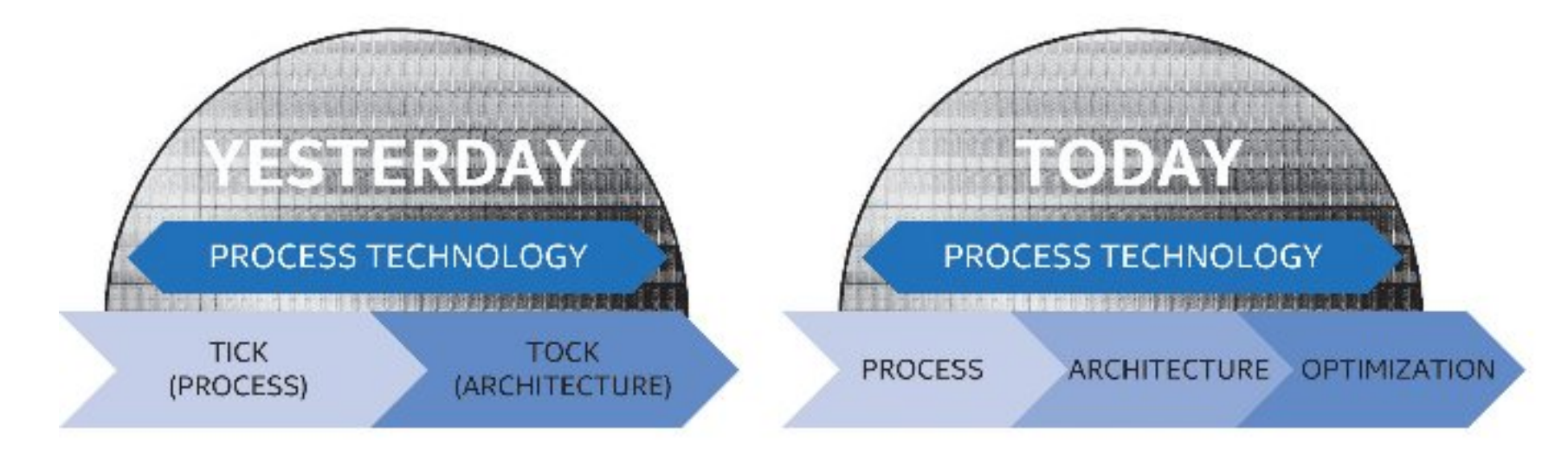
While the new PAO or ‘Performance-Architecture-Optimization’ model is a direct result of the complexity of developing and implementing new lithographic nodes (Intel has even entered into a new five-year agreement with ASML to develop new extreme-ultra-violet lithographic techniques), but also with new process nodes typically comes a time where yields have to become high enough to remain financially viable in the long term. It has been well documented that the complexity of Intel’s 14nm node using the latest generation FinFET technology took longer than expected to reach maturation point compared to 22nm. As a result, product launches were stretched out and within a three-year cycle Intel was starting to produce only two new generations of products.
Intel’s current in Ireland, Arizona, and Oregon are currently producing wafers on the 14nm node, with Israel joining Arizona and Oregon on the 22nm node. Intel also has agreements in place for third-party companies (such as Rockchip) to manufacture Intel’s parts for certain regional activity. As well as looking forward to 10nm, Intel’s filing also states projects in the work to move from 300mm wafers to 450mm wafers, reducing cost, although does not put a time frame on it.
The manufacturing lead Intel has had over the past few years over rivals such as Samsung, TSMC and Global Foundries, has put them in a commanding position in both home computing and enterprise. One could argue that by elongating the next two process nodes, Intel might lose ground on their advantage, especially as other companies start hitting their stride. However, the research gap is still there - Intel introduced 14nm back in August 2014, and has since released parts upwards of 400mm2, whereas Samsung 14nm / TSMC 16nm had to wait until the launch of the iPhone to see 100mm2 parts on the shelves, with Global Foundries still to launch their 14nm parts into products. While this relates to density, both power and performance are still considered to be on Intel’s side, especially for larger dies.
On the product side of things, Intel’s strategy of keeping the same microarchitecture for two generations allows its business customers to guarantee the lifetime of the halo platform, and maintain consistency with CPU sockets in both consumer and enterprise. Moving to a three stage cycle has thrown some uncertainty on this, depending on how much ‘optimization’ will go into the PAO stage: whether it will be microarchitectural, better voltage and thermal qualities, or if it will be graphics focused, or even if it will keep the same socket/chipset. This has a knock on effect with Intel’s motherboard partners, who have used the updated socket and chipset strategy every two generations as a spike in revenue.
Suggested Reading:
EUV Lithography Makes Good Progress, Still Not Ready for Prime Time
Tick Tock on the Rocks: Intel Delays 10nm, adds 3rd Gen 14nm
The Intel Skylake Mobile and Desktop Launch with Microarchitecture Analysis
More...
-
03-23-16, 08:01 AM #5853
Anandtech: The ADATA Premier SP550 SSD Review: A Second Look At Silicon Motion's SM22
Today we're taking a look at ADATA's Premier SP550 SSD, the company's latest entry-level drive. The Premier SP550 gives us a fresh look at Silicon Motion's SM2256 controller by pairing it with updated firmware and a different choice of TLC flash supplier. As an entry-level SSD it has very attractive pricing but no room to be skimping on performance.
More...
-
03-23-16, 09:15 AM #5854
Anandtech: Samsung Shows Off SM961 and PM961 SSDs: OEM Drives Get a Boost
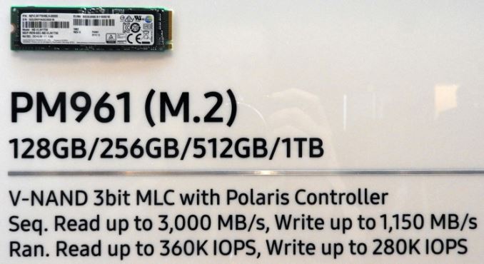
At Samsung's annual SSD Forum Japan, the company has demonstrated two previously-unannounced high-performance client SSDs. The new SM961 and the PM961 drives are based on the company’s Polaris controller as well as V-NAND flash memory. Samsung promises that the SSDs will increase sequential read speeds to 3000 – 3200 MB/s and will also significantly boost random read and write performance. The drives are projected to ship inside PCs in the second half of the year, while it's anyone's guess if and when these will filter into retail (ala the 950 series).
The Journey Continues
Samsung is the world’s largest producer of NAND flash memory and SSDs. Moreover, it is also one of the companies, which raise the bar of SSD performance and feature-set. In the recent years, Samsung has been an instrumental driving force in popularization of PCIe and NVMe SSDs. Samsung’s XP941 was one of the first high-end PCIe M.2 SSDs aimed at OEMs and it greatly helped to promote the form-factor among PC makers in 2014. The SM951 SSDs significantly increased performance of flash storage sub-systems compared to its predecessor and introduced NVMe to numerous OEMs a year later. In fall 2015, the Samsung 950 Pro finally brought NVMe and performance of the SM951 to retail market.
When introduced, the XP941 and the SM951 were for their respective times Samsung’s top-of-the-range SSDs designed for OEMs and their flagship PCs. Last year, the company decided to alter its strategy regarding high-performance SSDs aimed at PC makers. Instead of offering just one lineup of fast PCIe drives, Samsung introduced its second family of advanced SSDs with lower price and TLC NAND — the PM951. While the latter drives were still rather fast, the price/performance trade-off meant that they were considerably behind the SM951 in terms of sequential read and write speeds. This year, the company plans to change its approach to OEM SSDs once again. Samsung will offer two product families with slightly different characteristics: the SM961 and the PM961. The new lineups will further raise performance bar of Samsung's SSDs, but the PM961 is expected to make the new speed levels accessible to a broader audience. The tactics should help Samsung to increase its share of the premium SSD market.
Samsung SM961 and PM961: First to Use Polaris Controller
The new OEM SSD lineups from Samsung will be the company’s first standard high-end SSDs for PC makers, which use 3D/V-NAND memory. The new drives rely on the all-new Polaris platform and will come in M.2-2280 form-factor with PCIe 3.0 x4 interface while utilizing the NVMe protocol. Right now, the company is not revealing too many details about its new SSDs. For example, it is unknown whether they rely on Samsung’s third-gen 48-layer V-NAND or its second-gen 32-layer V-NAND. While using newer memory for new SSDs is logical, so far Samsung has not confirmed anything.
The Samsung SM961 will be Samsung’s new top-of-the-range M.2 SSD line for OEMs, which will be offered in 128 GB, 256 GB, 512 GB and 1 TB configurations (by contrast, the SM951 family did not include a 1 TB option). The drive will be based on Samsung’s MLC V-NAND as well as the company’s Polaris controller. Samsung is specing the SM961 at up to 3200 MB/s for sequential reads and up to 1800 MB/s for sequential writes, but does not specify which models will boast with such numbers. The new SSDs can perform up to 450K random read IOPS as well as up to 400K random write IOPS, which looks more like performance of server-grade SSDs.
The Samsung PM961 will be based on the company’s TLC V-NAND flash and the Polaris controller. The PM961 lineup will consist of four models: with 128 GB, 256 GB, 512 GB and 1 TB capacities (the PM951 also did not include a 1 TB model). The PM961 SSD supports sequential read speeds of up to 3000 MB/s as well as sequential write speeds of up to 1150 MB/s. Random read/write performance of the PM961 is up to 360K/280K of read/write IOPS, but Samsung does not specify exact models that offer such performance.
The PM961 should be more affordable than the SM961, but even with the use of TLC, according to Samsung's specifications it should be only slightly slower than the flagship model when it comes to sequential read speeds (6% difference is negligible). Sequential write speeds should be lower compared to those offered by the SM951 and the 950 Pro, but should still be considerably higher than sequential write speed of its direct predecessor, the PM951. Moreover, the new PM961 should also be considerably faster in random read and write operations versus its ancestors, according to specifications released by Samsung.
It remains to be seen how the PM961 drive will behave in real-world applications versus enthusiast-class PCIe SSDs from other manufacturers. But its 3000 MB/s sequential read performance as well as very high random reads and writes should probably play positive roles here.
Samsung has not formally introduced the SM961 and the PM961 SSDs, but PC Watch reports that the company expects computer makers to use the new drives in the second half of the year. Moreover, since the SSDs demonstrated at the event already feature actual labels with all the certification stamps and even serial numbers, it looks like development of the storage devices is very close to its completion.
Initially, Samsung will use its Polaris platform only for the drives intended for OEMs, but it is plausible to expect the company to utilize the same controllers for its retail SSDs eventually. As is usually the case, Samsung isn't commenting on whether we'll see retail Polaris drives in the future, though if 950 Pro is anything to go by, we wouldn't be surprised. Nonetheless, keeping in mind how easy is to get both SM951 and PM951 SSDs from stores like Amazon and RamCity, it should not be a problem to obtain these new OEM SSDs from online stores as well.Samsung SSD Comparison SM961 PM961 950 Pro
512 GBSM951-NVMe 512 GB (OEM) PM951-NVMe
512 GB (OEM)850 Pro
512 GBForm Factor M.2 2280 2.5" SATA Controller Samsung Polaris Samsung UBX unknown Samsung MEX Interface PCIe 3.0 x4 SATA III Protocol NVMe AHCI DRAM unknown 512 MB 512 MB 512 MB 512MB NAND Samsung
MLC V-NANDSamsung
TLC V-NANDSamsung V-NAND 32-layer 128Gbit MLC Samsung 16nm 64Gbit MLC Samsung TLC NAND flash Samsung V-NAND 32-layer 86Gbit MLC Sequential Read 3200 MB/s 3000 MB/s 2500 MB/s 2150 MB/s 1050 MB/s 550 MB/s Sequential Write 1800 MB/s 1150 MB/s 1500 MB/s 1550 MB/s 560 MB/s 520 MB/s 4KB Random Read (QD32) 450K IOPS 360K IOPS 300K IOPS 300K IOPS 250K IOPS 100K IOPS 4KB Random Write (QD32) 400K IOPS 280K IOPS 110K IOPS 100K IOPS 144K IOPS 90K IOPS Launch Date 2H 2016 October 2015 ~June 2015 2015 July 2014
Looking Ahead: PCIe 3.0 x4 May Become a New Performance Limiting Factor for SSDs
Looking at Samsung's specifications, it's interesting to note that the 3200 MB/s sequential read speed of the Samsung SM961 is very close to actual maximum bandwidth of the PCIe 3.0 x4 bus. A PCIe 3.0 connection supports transfer rates of 8 GT/s (GigaTransfers per second) per lane, for a total of 3.94 GB/sec for an x4 connection after factoring in overhead. As it appears, the bandwidth offered by four lanes of PCIe 3.0 - the maximum bus width supported by the M.2 standard - is close to being saturated by high-end client SSDs.
If this ends up being the case, then the SM961 may be Samsung’s fastest sequential transfer SSD for client PC applications for quite a while (i.e., until PCIe 4.0 arrives). Consequently, if the company plans to introduce its successors with the same PCIe 3.0 interface, it will have to improve other domains of SSD performance (e.g., performance in mixed workloads, endurance, power efficiency, etc.). Keeping in mind that Samsung’s retail 950 Pro SSDs were a little faster than the company’s SM951 despite using the same controller, it will be interesting to see how Samsung might differentiate its hypothetical enthusiast-oriented Polaris and MLC V-NAND-based SSD from its OEM offering (if such SSD is in the company’s plans at all, of course).
With that said, while certain Samsung’s SSDs may eventually hit a sequential transfer performance barrier in the form of PCIe 3.0 x4 bus, the bandwidth provided by this interface will still be enough for the vast majority of SSDs from different manufacturers going forward. Moreover, since real-world performance does not entirely depend on just sequential read or write speeds, there are a plenty of ways to improve performance of actual drives in real-world applications.
More...
-
03-23-16, 01:30 PM #5855
Anandtech: Samsung Readies New Cost-Effective SSDs Featuring Maia Controller
Thanks to introduction of the PCIe-based M.2 form-factor and subsequent removal of SATA III bandwidth constraints, the evolution of high-performance SSDs has been quite spectacular in the recent years. Nonetheless, there are plenty of SSDs which still rely on SATA and will continue to use SATA. Such devices can be used to upgrade previous-generation PCs or inside new low-cost notebooks. To address this market, Samsung has revealed that they are working on their all-new Maia controller and SSD platform for SATA, laying out how they intend to continue to evolve SATA SSDs.
The new Samsung Maia controller supports multiple types of NAND flash memory, including TLC and 3D NAND/V-NAND. At the Samsung SSD Forum Japan, the company demonstrated two new SSDs based on the Maia chip. Both drives come in 2.5” form-factor and with a SATA III (6Gbps) interface. Initially Samsung intends to use the controller to build drives for OEMs, but as is often the case with Samsung, it is quite possible that it will eventually show up in retail SSDs as well.
The new Samsung CM871a OEM SSD based on the Maia controller will feature Samsung’s 16nm TLC NAND, which indicates that the company has no plans to drop production of planar NAND flash memory for consumer SSDs any time soon. The drive is rated for maximum sequential read speed of up to 535 MB/s as well as sequential write speed of up to 215 MB/s in default mode or up to 515 MB/s with TurboWrite technology active. Like many modern TLC NAND-based SSDs, the CM871a uses part of the non-volatile memory in SLC mode for rapid caching. The SSDs can perform up to 97K random read IOPS as well as up to 59K random write IOPS (or 88K IOPS with TurboWrite technology). Samsung will offer its CM871a in 128 GB and 256 GB configurations, which indicates that the family was designed for the low end of the market.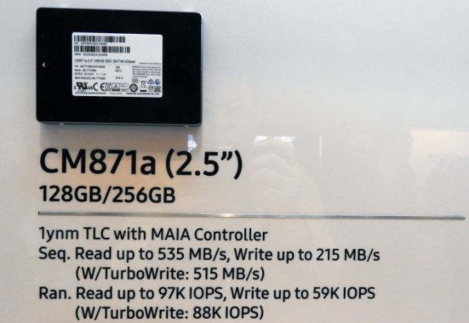
Meanwhile the Samsung PM871a will use the Maia controller alongside TLC V-NAND memory. According to Samsung, the drive has maximum sequential read speed of up to 530 MB/s and maximum sequential write speed of up to 515 MB/s (or up to 526 MB/s with TurboWrite). Random read performance of the PM871a is up to 97K, whereas random write performance of the drive is up to 88K IOPS. Samsung plans to offer its PM871a SSDs in 128 GB, 256 GB, 512 GB and 1 TB configurations. Samsung does not specify whether it utilizes its third-generation 48-layer V-NAND memory for the drives, or some drives continue to use previous-gen memory. While usage of 256 Gb TLC V-NAND for high-capacity SSDs makes a great sense, a 128 GB drive would in this case require only four such memory dies, limiting parallelism and is a solid example as to why manufacturers have been hesitant to produce small drives with cutting-edge high-density NAND.
These drives would be replacing Samsung's exisitng product line such as the PM871, which we have limited information about (given slow writes, it is logical to assume that it uses TLC NAND, but that is not something confirmed by Samsung). Meanwhile in the retail channel Samsung sells the inexpensive 850 EVO and 750 EVO SSDs. These SSDs are based on the company’s MGX controller, coupled with the company's second-gen 32-layer TLC V-NAND or 16 nm planar TLC, respectively. The aforementioned drives offer performance levels very similar to those of the forthcoming CM871a and PM871a, which may indicate that Samsung’s new Maia platform focuses mostly on cost efficiency, endurance and predictable performance, but not on maximum sequential read or random IOPS numbers (especially given limitations of SATA). Nonetheless, the development of Maia shows that SATA is still an important part of the market for Samsung as lower-end PCs continue to rely on it.Samsung SATA SSD Comparison Drive CM871a PM871a PM871
256 GB750 EVO
250 GB850 EVO
250 GBController Maia unknown MGX MGX NAND Samsung 16nm TLC Samsung TLC V-NAND unknown Samsung 16nm TLC Samsung 32-layer 128Gbit TLC V-NAND DRAM unknown 256MB 512MB Sequential Read 535 MB/s 530 MB/s 540 MB/s 540 MB/s 540 MB/s Sequential Write 215 MB/s
(515 MB/s with TurboWrite)515 MB/s
(526 MB/s with TurboWrite)280 MB/s 520 MB/s 520 MB/s 4KB Random Read 97K IOPS 97K IOPS unknown 97K IOPS 97K IOPS 4KB Random Write 59K IOPS
(88K with TurboWrite)88K IOPS unknown 88K IOPS 88K IOPS
More...
-
03-24-16, 02:36 AM #5856
Anandtech: Logitech Announces The Ambidextrous G900 Chaos Spectrum Gaming Mouse
Today Logitech is announcing the latest in their lineup of gaming mice. The G900 Chaos Spectrum is a wired and wireless mouse, and it is one of the few gaming mice which is ambidextrous. But it’s not just a vanilla mouse which can work in either hand, but instead it’s a mouse that can be customized to fit as either a left-handed or right-handed model.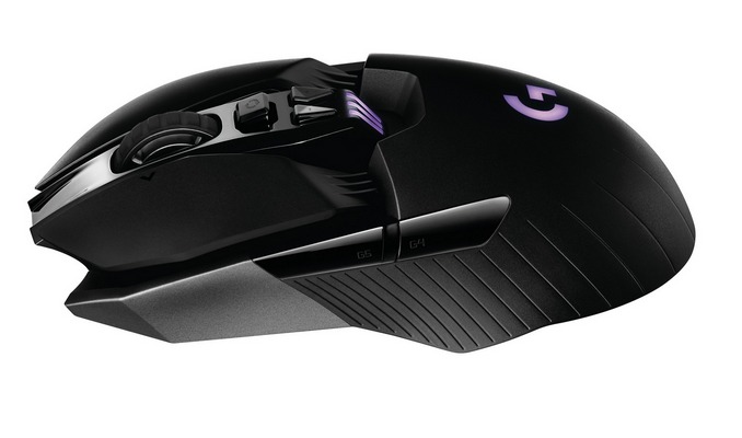
In addition, the mouse features customizable lighting with up to 16.8 million colors, and you can use the Logitech software to customize the lighting into breathing and other patterns. The software also allows you to calibrate the sensor against the surface you are going to use the mouse on, which should help with responsiveness.
As for the tracking capabilities, the G900 Chaos Spectrum mouse features the same PMW3366 optical sensor that Logitech features in some of their other mice. It offers 200 to 12,000 DPI and features zero smoothing or filtering across the range. Maximum acceleration is great than 40 Gs and the mouse can handle 300 inches per second of travel speed.
Logitech has designed a mechanical pivot for the buttons, which they state offer a crisp, clean click, and the metal spring tensioning reduces the amount of slack in the system before the buttons hit the actual switches. The buttons are rated for 20 million clicks. As with many of Logitech’s higher end mice, the scroll wheel is the fantastic hyper-fast scroll design. I’ve used a lot of mice, and I keep finding myself migrating back to Logitech for this feature alone.
The mouse is a wireless model, connecting over 2.4 GHz, and it can also be used as a wired mouse by connecting the cable on the front. This lets you charge while still using the mouse (amazingly not all mice do this even today) but either on wired or wireless, the G900 has the same 1000 Hz reporting rate. Logitech has put a lot of effort into power efficiency as well, and the G900 is rated for up to 32 hours of continuous use, or 24 hours with the default lighting enabled. That is impressive because the mouse weighs just 107 grams. If you go back in time to the Logitech G7 wireless gaming mouse, it offered two batteries and you’d be lucky to get through a single day without swapping the battery at least once.
The mouse has dimensions of 130 mm x 67 mm x 40 mm, and while this mouse doesn’t offer the massive button count that some games require, it does offer some unique features that should help set it apart from some of the other Logitech offerings, including the ability to configure the mouse for either left or right-handed grips.
The Logitech G900 Chaos Spectrum gaming mouse will go on sale in April, with a MSRP of $149.99.
Source: Logitech
More...
-
03-24-16, 08:27 AM #5857
Anandtech: Best CPUs: Q1 2016
When building a custom PC, especially on the consumer side, the processor is typically second or third down the list of priorities, behind graphics, storage or specific motherboard features depending on the use case. A lot of choosing a processor starts with the budget, if there is a preference for one brand or the other, or if the performance is similar enough that the money saved on a cheaper model can be spent elsewhere. By contrast, when it comes to workstations or enterprise situations, it helps to have an accurate profile of the intended workflow in order to choose which platform is needed, how much memory or how many expansion cards will be used, and if the software can prioritize cores over frequency or vice versa.
In our CPU Guide for Q1 2016, we’ll consider certain environments and budgets and give you our pick of some of the best processors available, supplying data from our Benchmark Database where possible.
If All You Need is Single Thread Performance:
Intel Pentium G3258 with an Overclock ($72 MSRP)
Some environments are single threaded by nature, such as single single-uses or basic home systems for email, writing reports or accessing the web. Even video streaming performance can benefit from single threaded speed in certain situations, so for this segment we’re going with the Pentium G3258. This is Intel’s overclockable dual core processor without hyperthreading, and comes out of the box at 3.2 GHz for only $72. In our review, with a good air cooler and some patience, we were able to extract 4.7 GHz stable with only a small increase in voltage, or 4.4 GHz was a nice point for power/voltage.
This makes it as fast as the Intel i7-4790K, Intel’s highest frequency consumer processor, in single threaded performance while costing ~$230 less when you also buy a reasonable cooler. Most motherboards will come with automatic overclock settings as well, making the job easier. On gaming, even when overclocked, the G3258 can fall behind on triple-A titles when equipped with a strong graphics card, which is something to note. The G3258 uses the Haswell platform and chipset, the 9-series (Z97), so there are a small number of USB 3.1 motherboards but full M.2 NVMe support will be limited. But if this is for a budget build, chances are M.2 NVMe won’t be high on the list anyway.
Buy Intel Pentium G3258 on Amazon.com
That Triple-A Gaming CPU for Single GPU Systems:
Intel i5-6600 ($213)
The nature of high end gaming is currently in a state of flux. Most of Intel’s quad-core processors do the job up to 4K single player gaming quite easily, with or without overclocks, and the i5-6600 is the one we’ve tested where it stands toe-to-toe with the larger i7 parts or the high-end desktop processors. The i5-6600 is a quad-core part without hyperthreading, starting at 3.3 GHz and pushing to a 3.9 GHz turbo for an official TDP of 65W.
The reason I say gaming is in flux is the big unknown in DirectX 12: as part of the DX12 platform, having more cores to perform asynchronous CPU physics or issue more kernel calls should help with graphics fidelity, making more complex scenes quicker to render: but will it allow simpler scenes to push 60, 90 or 120 frames per second? At this point, until some proper DX12 titles hit the market in full swing, we won’t know. What we do know is that for virtual reality, a modern Core i5 certainly fits the bill, especially in terms of latency to hit the 90 FPS quoted to ensure immersion without inducing nausea. For most current titles out however, the Core i5 will hit the asymptotic frame rate limit of a high-end GPU or be within 5-10% of it.
For users willing to push the boat for an overclock, the Core i5-6600K (at 3.5-3.9 GHz) is another $30 ($243). Many users consider Xeons for the i5-K part, and the most applicable one here is the E3-1230 v5 (at 3.4-3.8 GHz). At $250 it loses overclocking, high-speed memory and 100 MHz from the CPU frequency but enables hyperthreading, making it more like a Core i7-6700 but $50 cheaper. The only downside is that Intel’s Skylake Xeons require a server class chipset, the C232 and C236, which restricts motherboard choice.
Buy Intel Core i5-6600 on Amazon.com
Going for eSports without a Graphics Card:
AMD A10-7860K ($118) or Intel Core i5-5675C ($277)
My personal list of eSports or eSports-like titles comes in with DOTA 2, Counter Strike: Global Offensive, League of Legends and Rocket League. These titles are relatively simple to run on most graphics situations, and even when pushing the extreme details are fairly easy to render on any graphics card north of $150. This makes integrated graphics a nice entry point for users interested in eSports, allowing them to upgrade to a larger graphics card at a later date when they want to run the latest graphics cruncher. The two CPUs I’ve chosen here are the A10-7860K, one of AMD’s latest Kaveri Refresh parts that comes with a 95W cooler as standard and a really nice price, and the a king of integrated graphics in the Core i5-5765C, using 128MB of eDRAM to handily accelerate CPU-to-memory transfers which are vital in integrated graphics.
The A10-7860K from AMD is a new Kaveri Refresh part, replacing a few other older Kaveri units, but comes in with four threads, a full complement of eight compute units (512 SPs, the most we’ve seen on an APU), a 65W TDP, but is bundled with a 95W cooler as standard all for $118. Users can also look into overclocking this APU with that extra headroom, promising more performance. When we reviewed the A8-7670K with Rocket League, with 25% less GPU power we saw 1080p Medium settings going above a minimum 35 FPS, and with the A10 should be near a full 60 FPS average, especially with an overclock and/or fast memory.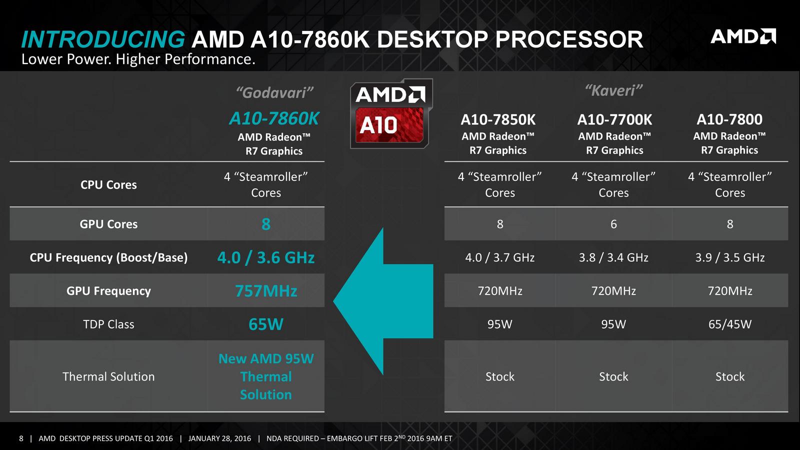
Buy AMD A10-7860K APU with R7 on Amazon.com
The Core i5-5675C from Intel uses two things: Intel’s largest integrated graphics on a desktop CPU, and 128MB of eDRAM as a quicker memory store to pull graphics and texture data from. With gaming, the bandwidth between the graphics cores and video memory is a vital factor in performance, and the eDRAM boosts the potential bandwidth from 25 GB/s on DDR3 to 50 GB/s bi-directional, while also decreasing latency. This eDRAM is part of Intel’s Crystalwell line, of which only two desktop parts have ever been released (and can be difficult to find). But when we reviewed both this i5 and the more expensive i7-5775C they came top of the roost for integrated graphics performance.
Buy Intel Core i5-5675C on Amazon.com
It is worth noting that DirectX 12 enables multi-adapter gaming, and if the game engine supports it, an integrated graphics unit can work with a discrete graphics card for improved gaming performance. So users investing in an eSports-focused integrated graphics system today and then a larger discrete graphics card for triple-A titles later might be able to take advantage of multi-adapter gaming on certain titles.
Going High End Desktop:
Intel Core i7-5820K ($396) or Intel Core i7-5960X ($999)
Sometimes all a consumer wants is power and cores. Without moving into the enterprise ecosystem for Xeons or Opterons, there are three real choices for a power user or prosumer. We reviewed the three Haswell-E Core i7 parts back in August in 2014, where an 8-core part, a 6-core part and a 6-core part with reduced PCIe lanes were put on sale. At the time we ended up with two suggestions: If you need 8 cores, then there’s only one choice in the i7-5960X, but if you just need DDR4 and are not strict on PCIe lanes then the i7-5820K performs the same as the mid-range part for $200 cheaper in dual GPU gaming at x16/x8 rather than x16/x16.
Buy Intel Core i7-5820K 6-Core on Amazon.com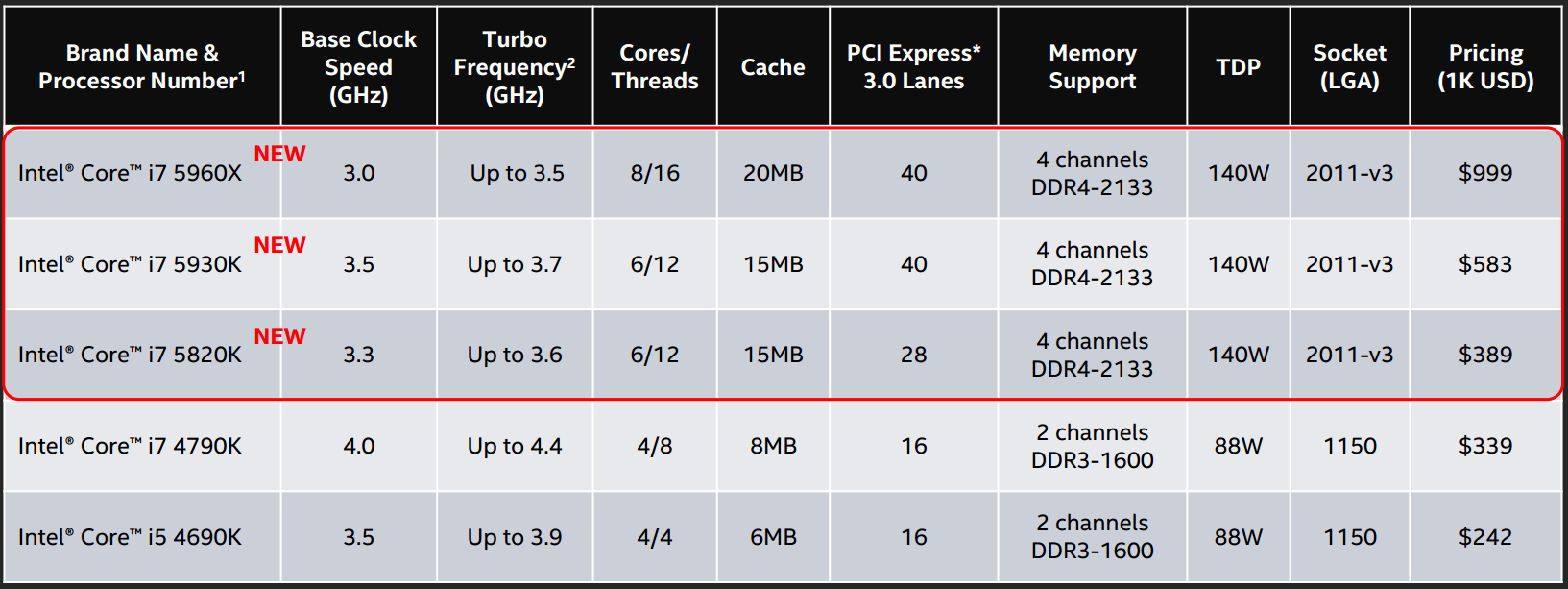
Buy Intel Core i7-5960X 8-Core on Amazon.com
The danger of suggesting these Haswell-E parts for the high-end desktop (HEDT) is that these parts are almost two years old, and no matter which way you slice it users are talking about when and where the Broadwell-E will be launched, and most arrows are pointing to mid-year. At this point the product line-up for Broadwell-E, along with the launch date, is all speculation. But we do know that they will be drop-in parts for the current crop of X99 motherboards, allowing users to invest in a Haswell-E system today and upgrade in the future (with a BIOS update).
A VR/Future Proof dual GPU System:
Intel i7-4790K ($350) or Intel Core i7-6700K ($350)
2016 is set to be the year when Virtual Reality gaming starts becoming ‘a thing’. We’ve done some beta testing of upcoming games, with headsets and titles almost ready to launch in a matter of weeks. One of critical points that both the Oculus Rift and HTC Vive will have to combat is the fact that (as quoted by several sources) only 1% of the current gaming PC community has enough grunt or the required connections to run a VR headset (compared to Playstation VR, where everyone has the hardware). Both Oculus and HTC have announced minimum specifications that all games will have to hit 90 FPS as a minimum to be considered ready for VR: this is typically a Core i5 processor and a GTX 970 or AMD R9 290 in tow, making the minimum price for a new VR build around $200 for the CPU and $300+ for the graphics card, plus another $300-$500 in other components. What if you’ve got a pair of high-end graphics cards ready to go? What CPU would give the most benefit here?
The simple answer here usually comes down to two choices – the latest Intel Skylake Core i7-6700K or the higher frequency and overclocking focused but slightly older Devil’s Canyon update in the Intel Core i7-4790K. Out of the box the i7-4790K has a higher turbo speed, but an older microarchitecture and both can be overclocked to around 4.7 GHz fairly easily as shown in our reviews. Because the i7-4790K is older, it can arguably found in bundles and cheaper than its original MSRP: $320 at Newegg and Amazon with cheaper Z97 motherboards compared to the inflated price of the i7-6700K which sits at $370-$374 with newer Z170 motherboards. If we’re going for future-proof, then the i7-6700K uses the 100-series chipsets on its motherboards, allowing for access to DDR4, M.2 PCIe 3.0 x4 support with NVMe, some motherboards with Thunderbolt 3 and USB 3.1, and the voltage regulator is back on the motherboard which has the potential to reduce heat issues.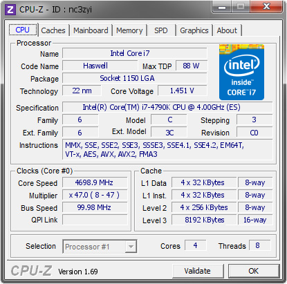
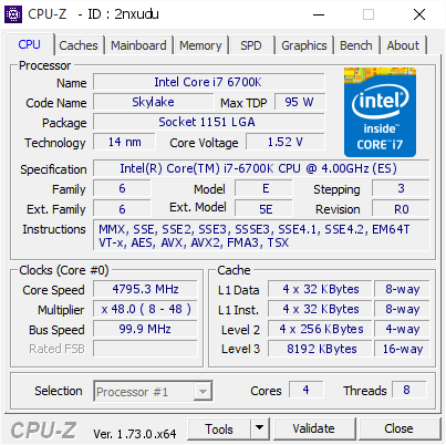
Core i7-4790K overclocked to 4.7 GHz (left)
Core i7-6700K overclocked to 4.8 GHz (right)
Buy Intel Core i7-4790K on Amazon.com
Buy Intel Core i7-6700K on Amazon.com
Using Handbrake converting a low-quality video as a benchmark that relies more on frequency and responsiveness, the testing doesn’t show much difference between the two processors at stock but both get a decent boost with the overclock, especially the i7-6700K. With the i7-6700K being more feature-packed I would perhaps be prepared to absorb the inflated price difference if I already had graphics cards on hand.
Honourable Mention for Price/Performance:
AMD Athlon X4 880K ($95)
For anyone building a budget conscious mid-range possible gaming system with a discrete graphics card, the upcoming Athlon X4 880K processor from AMD offers some nice value. Under the hood this is essentially a 100 MHz faster version of the A10-7870K which we reviewed, but as it does not have integrated graphics this allows all the power budget to be put squarely onto the overclockable CPU. Pairing it with a mid-range graphics card, such as the R9 380X or GTX 960 for around $200, makes a system easily capable of high-end graphics consistency on eSports titles and mid-range quality settings at 1080p for the major titles of the year.
The X4 880K also comes with AMD’s new 125W near-silent stock cooler, saving a few dollars. We put together a simple system: Athlon X4 880K, 2x8GB of G.Skill DDR3-2400, the new 480GB OCZ Trion 150 SSD, a GIGABYTE GTX 960 4GB, an EVGA 600W 80+ Bronze, a Corsair case and an ASRock FM2+ ATX motherboard for $634. Just add an operating system and it hits the price/performance curve at a nice spot.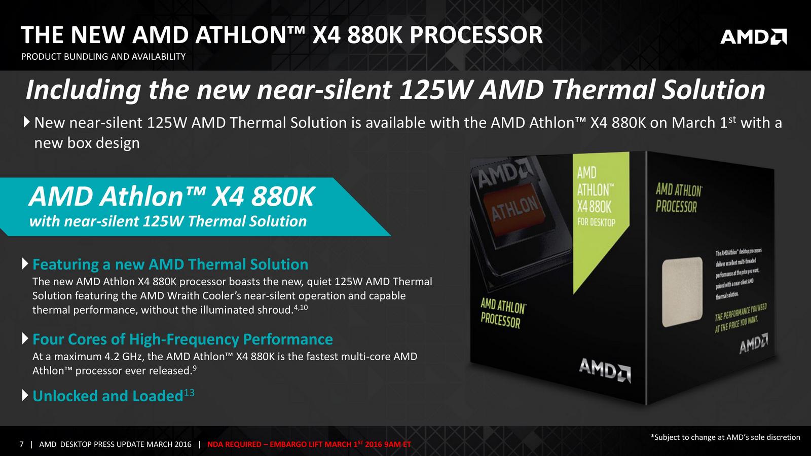
Buy AMD Athlon 880K on Amazon.com
Athlon X4 880 Mid-Range Build Part Price AMD Athlon X4 880K (with cooler) $95 ASRock FM2A88X Extreme4+ $75 G.Skill RipjawsX 2x8GB DDR3-2400 $63 OCZ Trion 150 SSD, 480GB $118 GIGABYTE GeForce GTX 960
Mini-ITX OC Edition, 4GB GDDR5$190 Corsair SPEC-01 RED Chassis $48 EVGA 600B 600W 80+ Bronze PSU $45 Total $634
Suggested Reading:
AnandTech’s Benchmark Database: Bench
AMD Launches the Athlon X4 880K: http://www.anandtech.com/show/10103/
Price Check: Intel’s Skylake CPUs: http://www.anandtech.com/show/10029/
AMD A8-7670K and Rocket League Review: http://www.anandtech.com/show/9763/
Intel Skylake Launch and Microarchitecture Analysis: http://www.anandtech.com/show/9582/
Intel i7-6700K Overclocking and Scaling Test: http://www.anandtech.com/show/9533/
Intel i7-6700K and i5-6600K Review: http://www.anandtech.com/show/9483/
Intel i7-5775C and i5-5675C Review Pt 2 (IPC): http://www.anandtech.com/show/9482/
Intel i7-5775C and i5-5675C Review Pt 1 (Perf): http://www.anandtech.com/show/9320/
AMD A10-7870K Review: http://www.anandtech.com/show/9307/
AMD A8-7650K Review: http://www.anandtech.com/show/9217/
AMD FX-8320E Review: http://www.anandtech.com/show/8864/
AMD FX-8370E Review: http://www.anandtech.com/show/8427/
Intel Haswell-E CPU Review: http://www.anandtech.com/show/8426/
AMD FX-9590 Review: http://www.anandtech.com/show/8316/
Intel Pentium G3258 Review: http://www.anandtech.com/show/8232/
Intel i7-4790K and i5-4690K (Devil’s Canyon) Review: http://www.anandtech.com/show/8227/
Intel Haswell Refresh Review: http://www.anandtech.com/show/7963/
More...
-
03-24-16, 12:32 PM #5858
Anandtech: Intel Quietly Speeds Up Skylake-U: i7-6660U now in Price List
Intel has quietly added a new Skylake-U processor into its price list. The new Intel Core i7-6660U system-on-chip is designed for low-power notebook systems and provides higher performance than its direct predecessor, the Core i7-6650U, and sits on the top of Intel's 15W mobile CPU stack.
The new Intel Core i7-6660U belongs to the Skylake-U family of processors that feature CPU and PCH on the same piece of substrate and are used to build mobile PCs with low power consumption. The new chip is currently only listed in Intel’s price list, which reveals its general specs (two cores with hyperthreading, 4 MB L3 cache and 2.40 GHz clock-rate, no word on turbo) as well as its price of $415 in 1000-unit quantities. The CPU costs the same amount of money as the Core i7-6650U and the Core i7-6560U.
If the Core i7-6660U chip shares general design with its predecessor, then it features two cores with Hyper-Threading technology clocked at 2.40 GHz (up 200 MHz from the i7-6650U), 4 MB L3 cache, a dual-channel memory controller (support for DDR4-2133, LPDDR3-1866 and DDR3L-1600 memory), Intel Iris Graphics 540 (48 execution units with 64 MB eDRAM, up to 1.05 GHz clock rate, up to 806.4 GFLOPS compute performance) as well as a 15 W TDP. The new processor should also support all the technologies that other Skylake-generation mobile Core i7 chips support, including AES-NI, AVX 2, vPro, virtualization (VT-x, VT-d), software guard extensions (SGX), TSX-NI, MPX, Trusted Execution, Secure Key, SSE4.1/4.2 and so on.
The quiet addition of the Core i7-6660U into the price list indicates that Intel is starting to gradually refresh its Skylake lineup of products. It is unclear whether the refresh is conditioned by the upcoming spring refresh cycle of PC makers or higher yields of chips produced using the 14 nm process technology. Nonetheless, the new CPU will help PC makers to differentiate their new offerings and speed up performance in certain applications.Intel Core i7 "Skylake-U" CPU Comparison Core i7-6660U Core i7-6650U Core i7-6600U Core i7-6500U Core i7-6567U Cores/Threads 2/4 Base Frequency 2.4 GHz 2.2 GHz 2.6 GHz 2.5 GHz 3.3 GHz Turbo Frequency unknown 3.4 GHz 3.4 GHz 3.1 GHz 3.6 GHz L2 Cache 256 KB x 2 (512 KB) L3 Cache 4 MB Memory Dual-channel DRAM controller with
DDR4-2133, LPDDR3-1866, DDR3L-1600 supportiGPU Iris Graphics 540 Iris Graphics 540 HD Graphics 520 HD Graphics 520 Iris Graphics 550 iGPU Config 48 EUs 24 EUs 48 EUs eDRAM 64 MB - 64 MB TDP 15 W 28 W Configurable TDP-down unknown 9.5 W 7.5 W 23 W Launch Q1 2016 Q3 2015 Price $415 $415 $393 $393 $415
Source: Intel Price List via CPU-World.
More...
-
03-25-16, 08:00 AM #5859
Anandtech: More Than Throughput: Next Generation Wi-Fi Testing with Ixia's WaveDevice
It’s been quite some time since I first started writing for AnandTech, and without question there’s been a lot of changes that have happened to our testing methodologies in the past few years. One of the main issues that I’ve always been thinking about while working through reviews is how we could improve our testing methodology in a meaningful way outside of simply updating benchmarks to stay current. Internally we’ve been investigating these issues for quite some time now, and these changes have included the addition of SoC power efficiency comparisons and display power efficiency measurements. There are a lot of other changes here and there that I still want to make, but one of the major unexplored areas has been wireless radio performance.
Wireless performance testing is probably one of the hardest things that we could test, and for a time I had almost given up hope on deploying such testing within AnandTech. However life has a way of playing out differently than I expect, and in the past few months we’ve been working with Ixia to make Wi-Fi testing a reality. Ixia, for those of our readers who aren't familiar with the company, is a traditional player in the networking test space. They are perhaps best known for their Ethernet test products, and more recently have been expanding into wireless and security testing with the acquisition of companies like VeriWave and BreakingPoint Systems.
We have done Wi-Fi testing before, but in the past we were mainly focused upon a relatively simple and arguably not particularly interesting test case: maximum throughput in ideal conditions. It was obvious that Wi-Fi in many devices is still not perfect, as subjective differences in reception and reliability can feel obvious. However, without any data or methods of replication it was hard to really prove that what we felt about wireless performance was really the case. To see how we've changed this, read on for the full article.
More...
-
03-25-16, 09:00 AM #5860
Anandtech: Toshiba to Build New Fab to Produce BiCS NAND Flash
Toshiba this month has announced plans to build a new manufacturing facility to produce its BiCS NAND flash memory. The company intends to start making chips at the new fab in 2018 and currently is not disclosing the planned production capacity of the factory. SanDisk yet has to confirm its participation in building the new fab, but the announcement itself means that despite an ongoing financial scandal, Toshiba is set to remain one the world’s largest makers of NAND flash memory.
Toshiba plans to invest around ¥360 billion ($3.233 billion) in its new facility in fiscal 2016 to fiscal 2018, with that price tag covering both construction costs and equipment investments. The fab will be located on land adjacent to the Yokkaichi Operations memory production complex in Mie prefecture, which means that the company essentially wants to add a new production complex to its Fab 5 (which is currently produces 2D NAND) and Fab 2. Exact decisions regarding construction schedule, manufacturing tools and other will be made in Toshiba’s fiscal 2016, which begins in April. Construction of a semiconductor manufacturing facility usually takes about a year. After the building is complete inside and outside, it takes about two or three quarters to move in equipment and start volume production. Therefore, Toshiba’s plan to begin operating the new facility in fiscal 2018 (which begins on April 1, 2018) seems viable.
The new fab will solely produce Toshiba’s 3D NAND memory, which the company calls BiCS (Bit Cost Scalable) NAND. Toshiba claims that the architecture of its proprietary BiCS NAND is more efficient in terms of die sizes compared to other types of 3D NAND thanks to its U-shaped NAND string. So far independent analysts have not verified whether Toshiba’s 48-layer 256 Gb TLC BiCS NAND chips are smaller or larger than Samsung’s 48-layer 256 Gb TLC V-NAND ICs, but if this proves to be the case, then Toshiba will enjoy lower production costs over time.
Meanwhile at present, Toshiba and SanDisk already operate multiple fabs for non-volitile memory, including the world’s largest NAND flash manufacturing facility, Fab 5 (phases 1 and 2) at the Yokkaichi Operations memory production complex in Mie Prefecture. Ahead of their newly announced fab for 2018, Toshiba and SanDisk are scheduled to produce their BiCS NAND memory at both Fab 2 and Fab 5 over the next year. BiCS production at Fab 2 is set for the first half of FY2016 (i.e., from April to October, 2016), and SanDisk has previously indicated that it would begin conversion of some of the capacity in Fab 5 to 3D NAND in 2016. Keeping in mind that SanDisk cannot do anything in the fab alone, it is clear that Toshiba and SanDisk have a plan to gradually convert the fab to 3D NAND in the future.
If Toshiba’s plan succeeds, by the second half of calendar 2018 it will have several semiconductor manufacturing facilities capable of producing BiCS NAND memory. While the combined manufacturing capacities of all three fabs are unknown at the moment, it is likely that the company will continue to produce vast amounts of NAND flash memory.
Toshiba said that it expected to continue its joint venture operation with SanDisk in expanding BiCS Flash capacity in the new facility. However, SanDisk is being acquired by Western Digital at the moment and it remains to be seen on what terms the new company will join Toshiba in investments.
Together, Toshiba and SanDisk currently make and sell more flash memory than Samsung, but keeping in mind how aggressively the latter plans to expand its semiconductor manufacturing capacities in the coming years, everything is subject to change. Last year Samsung announced plans to invest an additional $9.2 billion in expansion of its manufacturing facility near Pyeongtaek, South Korea. The latter will cost Samsung $14.4 billion and is scheduled to begin operations in 2017. While the fab is officially intended for DRAM production, its vast manufacturing capacities could be used to produce other types of semiconductors as well.
More...


 Quote
Quote
Thread Information
Users Browsing this Thread
There are currently 14 users browsing this thread. (0 members and 14 guests)


Bookmarks