

Results 6,211 to 6,220 of 12094
Thread: Anandtech News
-
08-16-16, 01:36 PM #6211
Anandtech: Intel Optane And 3D XPoint Updates From IDF
At Intel Developer Forum this week in San Francisco, Intel is sharing a few more details about its plans for their Optane SSDs using 3D XPoint memory.
The next milestone in 3D XPoint's journey to being a real product will be a cloud-based testbed for Optane SSDs. Intel will be giving enterprise customers free remote access to systems equipped with Optane SSDs so that they can benchmark how their software runs with 3D Xpoint-based storage and optimize it to take better advantage of the faster storage. By offering cloud-based access before even sampling Optane SSDs, Intel can keep 3D XPoint out of the hands of their competitors longer and perhaps make better use of limited supply while still enabling the software ecosystem to begin preparing for the revolution Intel is planning. However, this won't do much for customers who want to integrate and validate Optane SSDs with their existing hardware platforms and deployments.
The cloud-based Optane testbed will be available by the end of the year, suggesting that we might not be seeing any Optane SSDs in the wild this year. But at the same time, the testbed would only be worth providing if its performance characteristics are going to be pretty close to that of the final Optane SSD products. Having announced the Optane testbed like this, Intel will probably be encouraging their partners to share their performance findings with the public, so we should at least get some semi-independent testing results in a few months time.
In the meantime, Intel and ScaleMP will be demonstrating a use that Optane SSDs will be particularly well-suited for. ScaleMP's vSMP Foundation software family provides virtualization solutions for high performance computing applications. One of their specialities is providing VMs with far more virtual memory than the host system has DRAM, by transparently using NVMe SSDs—or even the DRAM and NVMe storage of other systems connected via Infiniband—to cache what doesn't fit in local DRAM. The latency advantages of 3D XPoint will make Optane SSDs far better swap devices than any flash-based SSDs, and the benefits should still be apparent even when some of that 3D XPoint memory is at the far end of an Infiniband link.
ScaleMP and Intel have previously demonstrated that flash-based NVMe SSDs can be used as a cost-effective alternative to building a server with extreme amounts of DRAM, and with a performance penalty that can be acceptably small. With Optane SSDs that performance penalty should be significantly smaller, widening the range of applications that can make use of this strategy.
Intel will also be demonstrating Optane SSDs used to provide read caching for cloud application or database servers running on Open Compute hardware platforms.
More...
-
08-16-16, 05:34 PM #6212
Anandtech: Intel Teases Mobile Kaby Lake: HEVC Main10 Profile Support, Coming This Au
During the Intel Keynote presentation today at IDF Brian Krzanich, CEO of Intel, demonstrated several upcoming Kaby Lake 2-in-1 prototypes from HP and Dell. While no concrete details about the 7th Generation of Intel Core products lines were given, we were offered a couple of bits of information to tide the hype until a full launch.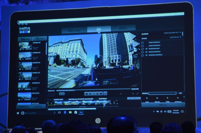
On the stage, support for HEVC Main10 Profile was announced with 7th Gen, although it was unclear if this was decode only or encode as well. This is still a step up from Skylake support, where Main10 required hybrid hardware/software decoding acceleration. Moving it into hardware for Kaby Lake will help with performance and power consumption, particularly of 4K content where HEVC vs. H.264 differences are bigger than Full-HD. The demo on stage showed GoPro software taking 4K data from six cameras and being able to switch between the content of each camera without stuttering or delay, on a 2-in-1 mobile device.
For gaming, we were treated to a demonstration of Overwatch being run off of the 7th Gen IGP. That being said, it was not mentioned what the resolution or quality the game was running at, and V-Sync was not enabled.
Intel clarified that the demos on the stage were from their highest performance CPUs, but the fact that only 2-in-1s were on display demonstrates that Kaby Lake will be focused on mobile first. The HP and Dell prototypes also add to the ASUS prototypes we saw at Computex earlier in the year. Intel stated that 7th Gen CPUs are already in the hands of partners, ready for production devices, and we should expect to see them in the hands of consumers this autumn. Again, given the focus, it seems we will encounter Kaby Lake in mobile form factors (4W and 15W) before anything on desktop.
More...
-
08-16-16, 07:01 PM #6213
Anandtech: Intel Announces Project Alloy: Untethered Augmented Reality in a VR Headse
During the Keynote today at IDF, Intel showed off the next play into the Virtual Reality design space. In an interesting twist, their new Project Alloy headset was demonstrated on stage and marketed as a fully untethered VR device that uses dual RealSense cameras to monitor location and position of objects around the user. The headset stills needs a PC for data transmission, such as the Skull Canyon NUC with Iris Pro graphics, but the idea to have a headset without wires is interesting but offers up a number of questions. On top of this, the Real Sense cameras will have full five-finger recognition, allowing the software to adjust the appearance of the users hands or other figures as appropriate (this is where the Augmented Reality comes in).
Intel mentioned that the headset has good weight distribution, as well as an SoC inside for the processing. There was no indication as to the power consumption of that SoC, but I can imagine it being under 10W otherwise it would heat up the users face over time. The back of the headset also has a compartment, which I would assume is battery, which gives another question on the battery life of such a headset.
The VR + AR concept is being marketed as ‘mixed reality’ – the ability to use your hands in a VR environment which also adjusts the visuals of your hands based on what is happening in the scene. In the demo on stage, Intel showed a hand turning into a skeleton hand when placed in front of an X-Ray scanner in the scene. There was also discussion that this sort of mixed reality (MR) allows full roaming capabilities that mean a user won’t easily bump into objects around their home (or walls).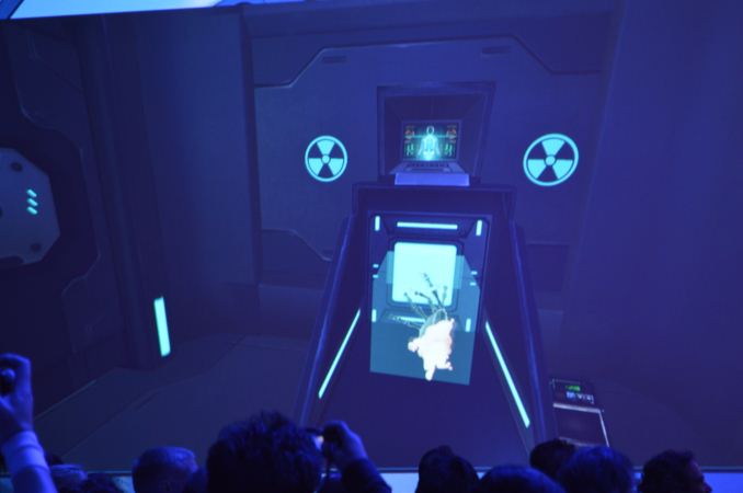
The demo was also projected onto a large screen, and it was clear this is still a prototype as we could see dropped frames. It was mentioned that Holo-Lens used Cherry Trail, and this is more powerful. Another element of use was a mix of 2D/3D environments, such as the eponymous ‘unlimited desktop’ for working and consuming content. The use of RealSense will be similar to at least one other headset with an external camera, but the rendered video on screen showed a person manipulating 2D interfaces projected onto walls with a remote control.
Project Alloy will require a Windows PC with Windows Holographic Platform, which will come to Windows 10 PCs next year as part of the regular updates. V1 of the device will be available to partners in December, and the hardware will be open sourced in the second half of 2017. The RealSense APIs will be opened up as well. Chances are we will see more demos this time next year.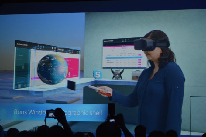
More...
-
-
08-17-16, 03:54 AM #6215
Anandtech: Intel Unveils Joule: An High-Perofrmance Atom-Powered IoT Module & Maker K
Today at Intel’s annual Developer Forum, the hardware manufacturer announced the latest in their Internet of Things-focused product kits: Joule. Based around Intel’s canceled-but-not-quite Broxton Atom processor, Joule is designed to further augment Intel’s existing lineup of kits by offering a much higher performance part based on the latest generations of the company’s technologies.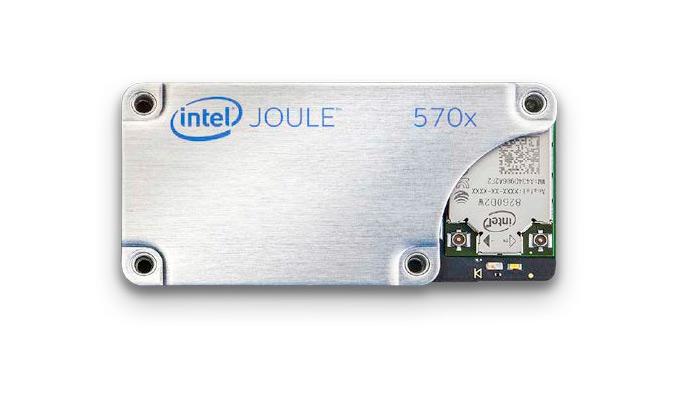
Back in 2013 Intel announced Galileo, the first of what has become a collection of IoT kits/platforms for hardware developers. Galileo and its compatriots Edison and Curie turned out to be solid hits for the company – even with competing kits already on the market – driving a big part of Intel’s overall IoT growth in recent years. The System on Module boards proved popular with tinkers and product developers alike who needed small systems for everything from small prototypes to a commercial off the shelf boards.
Joule then extends Intel’s presence in this market by offering a higher performing part in their IoT portfolio. Whereas the previous top-tier Edison board used a combination of Atom Silvermont and Quark CPU cores and paired this up with a respectable amount of RAM, NAND, and I/O options, Joule goes much further. The SoC at the heart of the board is Intel’s Broxton-M, which although was canceled for consumer devices, as we can now see will instead be making a home for itself within Intel’s IoT product family.Intel IoT Kits Joule 570X Joule 550X Edison SoC Intel Atom "Broxton-M"
T5700Intel Atom "Broxton-M"
T5500Intel Atom "Tangier"
Z34xxCPU 4x Goldmont @ 1.7GHz, Turbo to 2.4GHz 4x Goldmont @ 1.5GHz 2x Silvermont @ 500MHz
1x Quark @ 100MHzGPU Intel Gen9 Intel Gen9 N/A RAM 4GB LPDDR4 3GB LPDDR4 1GB LPDDR3 Storage 16GB eMMC 8GB eMMC 4GB eMMC Wireless 802.11ac w/MIMO + BT 4.1 802.11n + BT 4.0 I/O UART + GPIO + I2C + MPI CSI + MPI DSI + USB 3.0 SD + UART + SPI + GPIO + USB 2.0 OTG Dimentions 48 x 24 x 3.5 mm 35.5 x 25 x 3.9 mm
Intel is offering two different versions of the Joule board. Both use the same SoC, but they vary in clockspeeds and memory. The more powerful of the two, Joule 570X, uses what Intel is calling a Atom T5700, which is a quad core Goldmont Atom configuration with a base clock of 1.7GHz and can turbo to 2.4GHz. This in turn is paired with 4GB of LPDDR4 memory and a 16GB eMMC NAND module for non-volatile storage. Meanwhile the Joule 550X drops the quad core Atom to 1.5GHz with no turbo, and features 3GB of LPDDR4 memory along with 8GB of NAND.
Both Joule boards also feature the same I/O connectivity. On the wireless side, this is composed of a radio supporting Bluetooth 4.1 and 802.11ac (MIMO is listed supported, so I’m wagering this is a 2 spatial stream solution). And on the wired side, USB 3.0 is supported, along with the vast collection of GPIOs, UARTs, and MPI’s camera (CSI) and display (DSI) interfaces.
The Joule module itself is said to only be a bit larger than the Edison module – which was usually measured relative to a postage stamp – and in the brief glimpse of the module we got when Brian Krzanich held it out on stage, I’d say we’re looking at something not too much bigger than a stick of gum (or perhaps the old Sony memory stick). Intel hasn’t released the full documentation for the kit yet, so we don’t have power consumption information available, but given the higher performance goals for the kit (and the quad Goldmont CPU cores), it’s a fair bet that it’s going to be higher than Edison.
As you might expect from the specifications, Intel is aiming Joule at a higher performance class of use cases. Ultimately as a maker kit it’s a bit of an “if you build it” situation – it’s up to developers to figure out what to do with it – but Intel sees it as being useful for drones, AR/VR, robotics, and for the first time in one of their IoT products, computer vision. While we don’t have a ton of hard details on the underlying iGPU, it is powerful enough for certain CV tasks, and it supports both 4K video capture and display. It also supports Intel’s RealSense camera, giving developers the option of using the underlying depth sensing capabilities for improved vision/analysis.
Finally, on the software side of matters, the Joule will support a few different OSes. The boards will default to a new Linux distribution specifically designed for the hardware that Intel is calling Reference Linux OS for IoT, and Cannonical’s “Snappy” Ubuntu Core is also supported. Meanwhile Microsoft’s Windows 10 IoT Core is also supported for developers who need Windows interoperability.
Wrapping things up, along with today’s announcement, Intel has already begun selling one of the Joule SKUs, with the others to follow. The Joule 570X development kit, which includes the Joule module, carrier board, WiFi antennas, and other components is on sale today at IDF for $369, and will be available through Intel’s partners next month. At that price it’s fair to say that Intel is not aiming to have Joule compete with more mainstream kits – or even their own Edison kit – but rather at the more upscale kits such as the (even more expensive) NVIDIA Jetson TX1, which is a much tighter market in terms of the number of competitors.
Meanwhile the lower-end 550X development kit and the stand-alone Joule modules are scheduled for release in Q4. Pricing for those products has not yet been disclosed, though given the intent for Joule to be used in mass production devices, it’ll be interesting to see what Intel prices the stand-alone modules at.
More...
-
08-17-16, 04:39 PM #6216
Anandtech: Intel Announces Knights Mill: A Xeon Phi For Deep Learning
In a brief announcement as part of today’s Day 2 ketnote for IDF 2016, Intel has announced a new member of the Xeon Phi family. The new part, currently under the codename of Knights Mill, is being aimed at the deep learning market and is scheduled for release in 2017.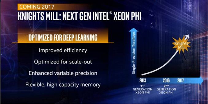
At this point there are more unknowns than knowns about Knights Mill, in part because Intel has not offered much detail on how it fits into the larger Xeon Phi brand. The company had previously announced in 2014 that the successor to the current Knights Landing design would be Knights Hill, a true 3rd gen Xeon Phi built on Intel’s 10nm process. However this week there has been no mention of Knights Hill, whether Knights Mill is Knights Hill renamed, or what the manufacturing process Knights Mill is being made on. With that said, as Knights Mill is scheduled for 2017, it’s unlikely that it’s Knights Hill (at least as initially planned), as 2017 would be too early for a very large 10nm chip from Intel’s fabs.
Working on the assumption at the moment that Knights Mill is in fact its own part, what we do know is that with it, Intel is making a very clear play for the rapidly growing machine learning market, and indeed this will be its defining characteristic. Among the features/design tweaks for the new processor, Intel is adding what they are calling “variable precision” support. What that fully entails isn’t clear, but the use of lower precision modes has been a major factor in the development and subsequent high performance of machine learning-focused processors, so it’s likely that this means that Intel is adding FP16 and possibly other lower-precision modes, something the current Knights Landing lacks. As machine learning typically does not require high precision, these lower precision modes potentially allow for a major increase in processor throughput, as more, narrower operations can be packed into a SIMD.
Announced In 2014 And Currently MIA: Knights Hill
Also on the feature list is improved scale-out performance. It’s not clear right now if this is some kind of fabric/interconnect change, or if Intel has something else in mind. But the ultimate goal is to make clusters of Xeon Phi processors perform better, which is an important factor in bringing down the training time of very large and complex datasets. Meanwhile there are also unspecified memory changes for Knights Mill, with Intel touting the chip’s “flexible, high capacity memory.”
Competitively, this is a shot across the bow at NVIDIA’s own Tesla products, and in their comments here at IDF and in previous presentations, Intel has not shied away from comparing their tech to GPUs and touting why they believe Xeon Phi to be superior. One such example, though briefly mentioned, is that like Knights Landing, Knights Mill is capable of acting as a host processor. So expect to see Intel promoting the benefits of not needing separate host processors & co-processors, and how Knights Mill can be attached directly to system RAM. This, along with the performance differences between the GPU architectures and Knights Mill, will undoubtedly be a recurring fight between the two companies both now and next year when the new processor actually launches.
In the meantime, we’ll keep digging for more information on Knights Mill, and hopefully get a better idea of how it fits into the Xeon Phi family.
(Image Courtesy The Register)
More...
-
08-17-16, 06:36 PM #6217
Anandtech: Marvell Announces NVMe Controller for DRAM-Less PCIe 3.0 x2 SSDs
Marvell has announced its new controller for affordable and miniature SSDs, the 88NV1160. The chip can be used to build small form-factor SSDs in M.2 as well as BGA packages. The 88NV1160 supports all modern and upcoming types of NAND flash, LDPC error correction, NVMe protocol and other advantages of modern SSD controllers, but it does not require external DRAM buffers so to reduce BOM costs of upcoming SSDs.
The Marvell 88NV1160 is a quad-channel controller that supports PCIe 3.0 x2 interface, NVMe 1.3 protocol (in addition to AHCI) as well as various types of NAND flash memory, including 15 nm TLC, 3D TLC as well as 3D QLC with ONFI 3.0 interface with up to 400 MT/s transfer rates. The 88NV1160 controller is powered by dual-core ARM Cortex-R5 CPUs along with embedded SRAM with hardware accelerators to optimize IOPS performance. The chip supports Marvell’s third-generation LDPC error correction technology (which the company calls NANDEdge ECC) in a bid to enable high endurance of drives featuring ultra-thin TLC or 3D QLC memory.
The 88NV1160 controller is specifically tailored for upcoming affordable SSDs, which is why it does not officially support SLC and 2D MLC NAND. Maximum capacity of a 3D QLC-based SSD featuring the 88NV1160 controller is expected to be around 1 TB, which should be enough for entry-level SSDs (as well as solid-state storage solutions for premium tablets, ultrabooks and other types of computing devices). As for performance, Marvell mentioned 1600 MB/s maximum read speed for such SSDs.Specifications of Marvell 88NV1160 at Glance Compute Cores Two ARM Cortex-R5 Host Interface PCIe 3.0 x2 Protocol of Host Interface AHCI, NVMe 1.3 Supported NAND Flash Types 15 nm TLC
3D TLC
3D QLCSupported NAND Flash Interfaces Toggle 2.0 and ONFi 3.0, up to 400 MT/s Page Sizes Unknown Number of NAND Channels 4 channels with 4 CE per channel (16 targets in total) ECC Technology LDPC (third-generation LDPC ECC by Marvell) Maximum SSD Capacity 1024 GB (when using 3D QLC ICs with 512 Gb capacity) Maximum Sequential Read Speed 1600 MB/s Maximum Sequential Write Speed Unknown, depends on exact type of memory Power Management Low power management (L1.2) design Package 9 × 10 mm TFBGA package Voltages 3.3V/1.8V/1.2V power supply (according to M.2 specs)
The new chip from Marvell is made using 28 nm process technology and is shipped in 9 × 10 mm TFBGA package, which can be used to build SSDs in BGA (M.2-1620 and smaller) packages as well as drives in M.2-2230/2242 form-factors. The 88NV1160 controller uses 3.3V/1.8V/1.2V power supply, in accordance with the M.2 standards.
The 88NV1160 is not the first controller from Marvell that does not require any external DRAM buffers. The company also offers low-cost 88NV1120 with SATA interface as well as 88NV1140 for PCIe 3.0 x1 SSDs. All of the aforementioned controllers are based on two ARM Cortex-R5 cores, feature Marvell’s third-gen LDPC implementation and support modern types of NAND flash memory (15nm 2D TLC and 3D TLC/QLC). However, the new 88NV1160 is the newest DRAM-less controller from the company, which is designed for rather advanced SSDs with up to 1600 MB/s read speed. Still, the 88NV1160 is clearly a solution for affordable drives because unlike the high-end 88SS1093 (or its less advanced brother, the 88SS1094) it does not support 2D MLC and SLC NAND flash and cannot take advantage of eight NAND channels (which is why it does not need PCIe 3.0 x4).
The developer did not reveal when it expects the first SSDs based on the 88NV1160 controller to hit the market, but it indicated that the chip is available for sampling globally. In addition, the company indicated that it offers turnkey firmware to its customers so to enable faster time to market.Comparison of Modern SSD Controllers from Marvell 88NV1120 88NV1140 88NV1160 88SS1093 Compute Cores Two ARM Cortex-R5 Three cores Host Interface SATA PCIe 3.0 x1 PCIe 3.0 x2 PCIe 3.0 x4 Protocol of Host Interface AHCI AHCI, NVMe 1.3 NVMe 1.1 Supported NAND Flash Types 15 nm TLC
3D TLC
3D QLC15 nm SLC/MLC/TLC
3D NANDNumber of NAND Channels 2 channels
4 CE per channel (8 targets in total)4 channels
4 CE per channel (16 targets in total)8 channels
4 CE per channel (32 targets in total)ECC Technology Marvell's third-gen LDPC-based ECC technology Host Memory Buffer No Yes Yes - Package 8 × 8 mm
TFBGA9 × 10 mm
TFBGABGA Compatibility M.2/BGA SSDs M.2/2.5" SSDs
More...
-
08-18-16, 07:25 AM #6218
Anandtech: More Details on Broxton: Quad Core, ECC, Up to 18 EUs of Gen9
An interesting talk regarding the IoT aspects of Intel’s Next Generation Atom Core, Goldmont, and the Broxton SoCs for the market offered a good chunk of information regarding the implementations of the Broxton-M platform. Users may remember the Broxton name from the cancelled family of smartphone SoCs several months ago, but the core design and SoC integration is still mightily relevant for IoT and mini-PCs, as well as being at the heart of Intel’s new IoT platform based on Joule which was announced at IDF this week as well.
Broxton in the form that was described to us will follow the previous Braswell platform in the sense that it runs in a quad-core configuration (for most SKUs) consisting of two sets of dual cores sharing a common L3 cache, but will be paired with Intel’s Gen9 graphics. The GPU configuration will be either in a 12 execution unit (EU) or 18 EU format, suggesting that the core will have a single graphics slice and will implement Intel’s binning strategy to determine which EUs are used on each sub-slice.
It was listed that Broxton will support VP9 encode and decode, as well as H.264. HEVC will be decode but they were hazy in clarifying decode support, saying that ‘currently we have a hybrid situation but this will change in the future’. There will also be OpenCV libraries available for Computer Vision type workloads to take advantage of optimized libraries that focus specifically on the graphics architecture.
It’s worth noting that on this next slide it notes the memory controller supporting DDR3L and LPDDR4, and later on in the presentation it only stated DDR3L. We asked about this, and were told that LPDDR4 was in the initial design specification, but may or may not be in a final product (or only in certain SKUs). However, DDR3L is guaranteed.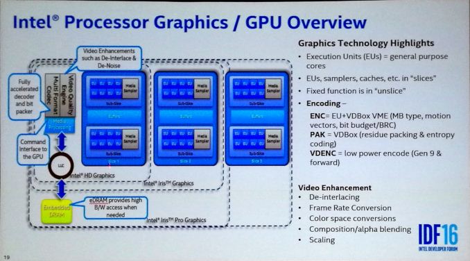
It was confirmed that Broxton is to be produced on Intel’s 14nm process, featuring a Gen9 GPU with 4K encode and decode support for HEVC (though not if this is hardware accelerated or hybrid or not). The graphics part will feature an upgraded image processing unit, which will be different to other Gen9 implementations, and we will see the return of extended temperature processors (-40C to 110C) for embedded applications.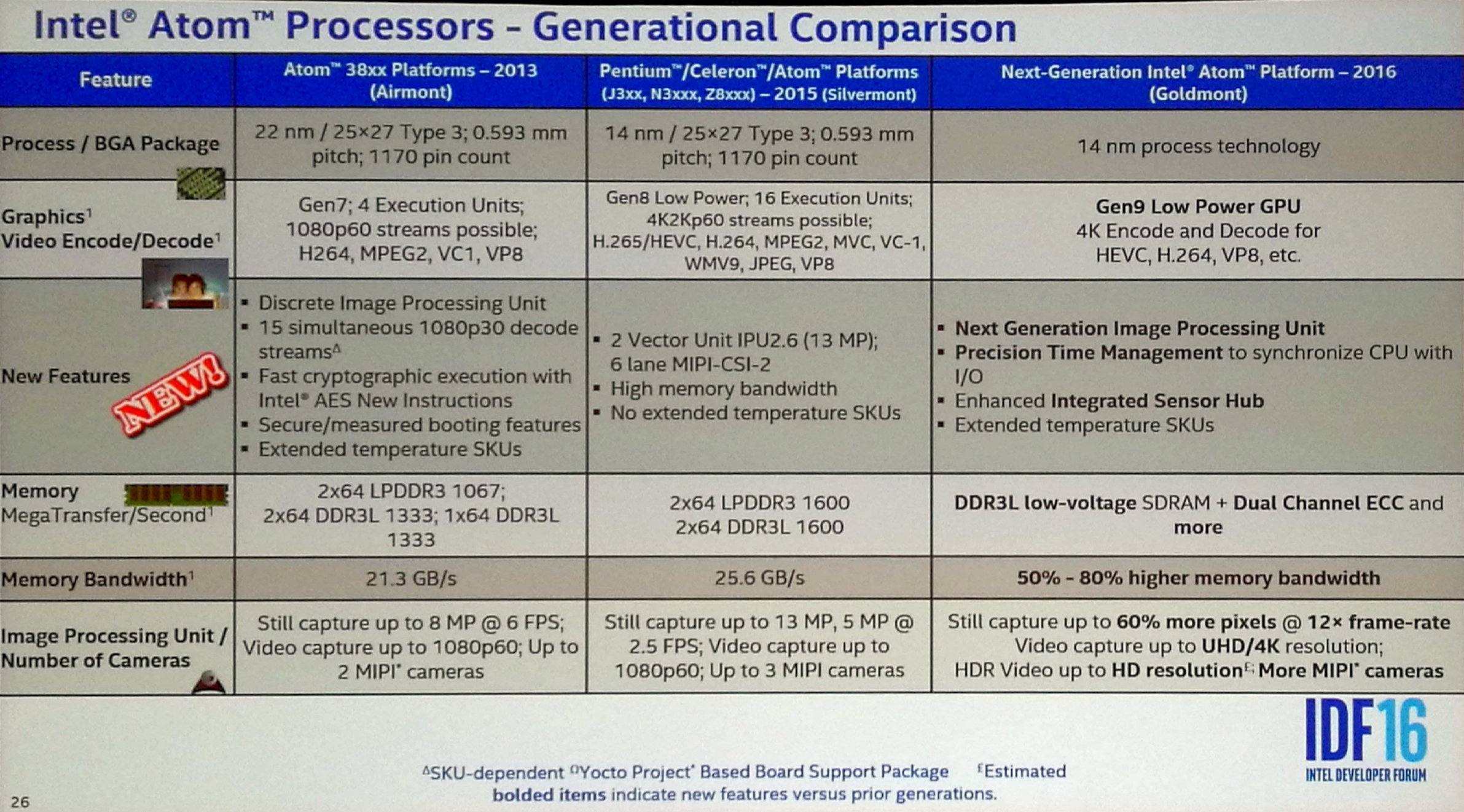
One of the big plus points for Broxton will be the support of dual channel ECC memory. This opens up a few more markets where ECC is a fundamental requirement to the operation. The slides also state a 50-80% higher memory bandwidth over Braswell, which is an interesting statement if the platform does not support LPDDR4 (or it’s a statement limited to the specific SKUs where LPDDR4 is supported).
All the displays from the Broxton SoC will support 4K60 outputs on eDP and DP/HDMI, along with more USB ports and support for eMMC 5.0. The support for 4K on HDMI might suggest full HDMI 2.0 support, however it is not clear if this is 4:2:0 chroma support or higher. The Broxton SKUs in this presentation were described as having a 6-12W TDP, with support on a number of Linux flavors, Android, and Windows 10. We asked about Windows 7 support, and we were told that while Broxton will likely support it, given the limited timeframe it is not expected to be promoted as a feature. We asked other questions on frequency, and were told to expect quad-core parts perhaps around 1.8-2.6 GHz. This would be in line with what we expect – a small bump over Braswell.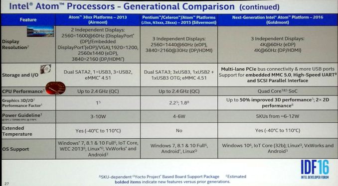
We are still waiting on more detailed information regarding Goldmont and Goldmont-based SoCs like Broxton, and will likely have to wait until they enter the market before the full ecosystem of products is announced.
More...
-
08-18-16, 07:25 AM #6219
Anandtech: Micron Cancels Ballistix TX3 NVMe SSD
At Computex in June, Micron announced that Crucial's Ballistix brand was being promoted to a standalone brand for gaming-oriented products. Their exhibit included three tiers of Ballistix DRAM products and one SSD: the Ballistix TX3 M.2 PCIe SSD. Based on Micron 3D MLC NAND and the Silicon Motion SM2260 NVMe SSD controller, the TX3 was to be Micron's first consumer/retail SSD with 3D MLC or a PCIe interface and was slated for a release sometime in the second half of 2016.
Micron has informed us this week that the Ballistix TX3 program has been canceled. This leaves Micron's consumer SSD strategy up in the air. With the release this summer of the Crucial MX300, Micron moved their mainstream SATA MX line from MLC to 3D TLC NAND, casting doubt on the future of the value-oriented BX series and implying that their 3D MLC might be regarded as premium enough to be reserved for PCIe SSD. With the Ballistix TX3 canceled, we no longer have any clear indication of how Micron plans to move forward with their consumer SSD products.
Micron may have decided to switch SSD controllers. While Silicon Motion reported last week at Flash Memory Summit that final firmware for the SM2260 controller is ready, Phison's E7 controller is also available and ready to roll out, and Micron has been shipping Marvell's 88SS1093 NVMe controller on their 7100 series enterprise SSDs in both U.2 and M.2 form factors, albeit with planar MLC NAND rather than their 3D NAND. Micron may also have decided that the timing was wrong to be getting into a market segment that Samsung has been handily dominating; beating Samsung's PCIe M.2 drives on performance will be an uphill battle to say the least, and substantially undercutting them on price may not be possible while Micron is still ramping up production of their 3D MLC NAND.
Micron's OEM and enterprise offerings may offer some clues to their plans, but the Micron and Crucial SSD product lines are no longer mere alter egos of each other. Micron's 1100 series SATA SSD is the nearest equivalent to the MX300 with the same controller and same 3D TLC NAND, but the 1100 is more a little more conservative by retaining the traditional power of two drive capacities with generous overprovisioning while the MX300 dedicates some of the extra capacity of Micron's 3D TLC chips to increasing the usable drive capacity.
Micron announced a 2100 series at the same time as the 1100 series, but did not provide full details as it was scheduled for a later introduction than the 1100, but still by the end of summer this year. The photos provided of the 2100 clearly showed the Silicon Motion SM2260 controller and the drive was stated to be using 3D NAND, but whether it would be MLC or TLC was not specified. The layout of the 2100 M.2 card was different than that of the Ballistix TX3 prototypes shown at Computex, but they still clearly had a few things in common. Micron's website still lists the 2100 as "Coming Summer 2016", and with regards to its fate Micron had this statement for us:
Micron is committed to delivering client PCIe NVMe solutions. While we are excited by the possibilities with our OEM partners, we are not disclosing availability details at this time. We will be sure to keep you updated as we are ready to share more.We are eager to hear what Micron decides to do, as they are still only the second manufacturer to deliver 3D NAND for the client and consumer SSD market and we have not yet had the chance to test their 3D MLC NAND. Competition in the consumer PCIe SSD space will be heating up with or without Micron's participation as more drives based on Phison, Marvell and Silicon Motion PCIe NVMe controllers hit the market over the next few months, but Micron's entry was particularly promising for the inclusion of 3D NAND.
More...
-
08-18-16, 08:16 AM #6220
Anandtech: AMD Zen Microarchitecture: Dual Schedulers, Micro-Op Cache and Memory Hier
In their own side event this week, AMD invited select members of the press and analysts to come and discuss the next layer of Zen details. In this piece, we’re discussing the microarchitecture announcements that were made, as well as a look to see how this compares to previous generations of AMD core designs.
More...


 Quote
QuoteThread Information
Users Browsing this Thread
There are currently 14 users browsing this thread. (0 members and 14 guests)


Bookmarks