

Results 6,341 to 6,350 of 12094
Thread: Anandtech News
-
09-28-16, 07:00 AM #6341
Anandtech: NVIDIA Teases Xavier, a High-Performance ARM SoC for Drive PX & AI
Ever since NVIDIA bowed out of the highly competitive (and high pressure) market for mobile ARM SoCs, there has been quite a bit of speculation over what would happen with NVIDIA’s SoC business. With the company enjoying a good degree of success with projects like the Drive system and Jetson, signs have pointed towards NVIDIA continuing their SoC efforts. But in what direction they would go remained a mystery, as the public roadmap ended with the current-generation Parker SoC. However we finally have an answer to that, and the answer is Xavier.
At NVIDIA’s GTC Europe 2016 conference this morning, the company has teased just a bit of information on the next generation Tegra SoC, which the company is calling Xavier (ed: in keeping with comic book codenames, this is Professor Xavier of the X-Men). Details on the chip are light – the chip won’t even sample until over a year from now – but NVIDIA has laid out just enough information to make it clear that the Tegra group has left mobile behind for good, and now the company is focused on high performance SoCs for cars and other devices further up the power/performance spectrum.
So what’s Xavier? In a nutshell, it’s the next generation of Tegra, done bigger and badder. NVIDIA is essentially aiming to capture much of the complete Drive PX 2 system’s computational power (2x SoC + 2x dGPU) on a single SoC. This SoC will have 7 billion transistors – about as many as a GP104 GPU – and will be built on TSMC’s 16nm FinFET+ process. (To put this in perspective, at GP104-like transistor density, we'd be looking at an SoC nearly 300mm2 big)NVIDIA ARM SoCs Xavier Parker Erista (Tegra X1) CPU 8x NVIDIA Custom ARM 2x NVIDIA Denver +
4x ARM Cortex-A574x ARM Cortex-A57 +
4x ARM Cortex-A53GPU Volta, 512 CUDA Cores Pascal, 256 CUDA Cores Maxwell, 256 CUDA Cores Memory ? LPDDR4, 128-bit Bus LPDDR3, 64-bit Bus Video Processing 7680x4320 Encode & Decode 3840x2160p60 Decode
3840x2160p60 Encode3840x2160p60 Decode
3840x2160p30 EncodeTransistors 7B ? ? Manufacturing Process TSMC 16nm FinFET+ TSMC 16nm FinFET+ TSMC 20nm Planar
Under the hood NVIDIA has revealed just a bit of information of what to expect. The CPU will be composed of 8 custom ARM cores. The name “Denver” wasn’t used in this presentation, so at this point it’s anyone’s guess whether this is Denver 3 or another new design altogether. Meanwhile on the GPU side, we’ll be looking at a Volta-generation design with 512 CUDA Cores. Unfortunately we don’t know anything substantial about Volta at this time; the architecture was bumped further down NVIDIA’s previous roadmaps for Pascal, and as Pascal just launched in the last few months, NVIDIA hasn’t said anything further about it.
Meanwhile NVIDIA’s performance expectations for Xavier are significant. As mentioned before, the company wants to condense much of Drive PX 2 into a single chip. With Xavier, NVIDIA wants to get to 20 Deep Learning Tera-Ops (DL TOPS), which is a metric for measuring 8-bit Integer operations. 20 DL TOPS happens to be what Drive PX 2 can hit, and about 43% of what NVIDIA’s flagship Tesla P40 can offer in a 250W card. And perhaps more surprising still, NVIDIA wants to do this all at 20W, or 1 DL TOPS-per-watt, which is one-quarter of the power consumption of Drive PX 2, a lofty goal given that this is based on the same 16nm process as Pascal and all of the Drive PX 2’s various processors.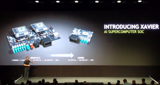
NVIDIA’s envisioned application for Xavier, as you might expect, is focused on further ramping up their automotive business. They are pitching Xavier as an “AI Supercomputer” in relation to its planned high INT8 performance, which in turn is a key component of fast neural network inferencing. What NVIDIA is essentially proposing then is a beast of an inference processor, one that unlike their Tesla discrete GPUs can function on a stand-alone basis. Coupled with this will be some new computer vision hardware to feed Xavier, including a pair of 8K video processors and what NVIDIA is calling a “new computer vision accelerator.”
Wrapping things up, as we mentioned before, Xavier is a far future product for NVIDIA. While the company is teasing it today, the SoC won’t begin sampling until Q4 of 2017, and that in turn implies that volume shipments won’t even be until 2018. But with that said, with their new focus on the automotive market, NVIDIA has shifted from an industry of agile competitors and cut-throat competition, to one where their customers would like as much of a heads up as possible. So these kinds of early announcements are likely going to become par for the course for NVIDIA.
More...
-
09-28-16, 01:32 PM #6342
Anandtech: BlackBerry Stops Development of Smartphones, Set to Outsource Hardware Dev
BlackBerry on Wednesday said it would cease internal development of its hardware and will transfer that function to its partners. While the BlackBerry-branded devices will remain on the market, BlackBerry itself will focus completely on software and will not invest in development of devices. The move edges the company closer to exiting the hardware business after years of considering such a move.
“The company plans to end all internal hardware development and will outsource that function to partners,” said John Chen, CEO and chairman of BlackBerry. “This allows us to reduce capital requirements and enhance return on invested capital," continued Chen.
Less than three years ago BlackBerry inked a strategic partnership with Foxconn, under which the two companies jointly developed certain BlackBerry-branded smartphones. Foxconn then built the hardware and managed the entire inventory associated with these devices. Now, the company intends to cease all of its hardware-related R&D activities and outsource this function to others.BlackBerry will now focus on development of extra-secured versions of Google’s Android operating system (recently the company introduced its own version of Android 6.0 that is used on the DTEK50 smartphone) as well as applications with enhanced security available through its BlackBerry Hub+ service.
In addition to Foxconn, BlackBerry has worked with other hardware makers. BlackBerry’s DTEK50 smartphone released earlier this year resembles Alcatel’s Idol 4 handset developed by Chinese TCL. Therefore, right now BlackBerry has at least two partners, which can build smartphones carrying the well-known brand all by themselves. In fact, this deal with BlackBerry puts TCL into an interesting position because it now can make handsets both under BlackBerry and Palm brands.
Today, BlackBerry also announced its first licensing agreement with joint venture PT Merah Putih, an Indonesia-based company. Under the terms of the agreement, the latter manages production and distribution of BlackBerry-branded devices running the BlackBerry’s Android software. While it is not completely clear to which degree PT Merah Putih develops its hardware in-house (typically, such companies outsource design of their products to others), it is more than likely that the actual devices are made by an ODM, such as Foxconn or TCL.
BlackBerry has been considering an exit from the hardware business for several years now, ever since the company appointed John Chen as CEO. The head of the company has said on multiple occasions that software and security technologies are the main strength for BlackBerry and warned that the firm could drop hardware completely if this business is not profitable. As it appears, BlackBerry will cease development of its smartphones, but will allow others to do it. Therefore, BlackBerry-branded devices will remain on the market, but the company will not spend big money on their development.
More...
-
09-29-16, 10:38 AM #6343
Anandtech: The Lenovo ThinkPad X1 Yoga Review: OLED and LCD Tested
Earlier this year at CES, Lenovo took the wraps off their latest lineup of premium business class notebooks, and they revamped the X1 lineup completely. Originally the X1 was just the X1 Carbon notebook, but Lenovo has decided to expand the X1 series to include the X1 Carbon, the X1 Yoga and X1 Tablet. So the ThinkPad Yoga is now the ThinkPad X1 Yoga, and as such it keeps the same thin and light design of the X1 Carbon.
More...
-
09-29-16, 02:57 PM #6344
Anandtech: Giveaway: OCZ VX500 & RD400 SSDs
It’s been a while since we’ve last had a hardware giveaway, so for those of you looking for some new hardware, you’re in luck. As part of the recent launch of our updated forums, the forum community team will be holding an Ask The Experts-styled Q&A session with OCZ, and along with that will be giving away a few OCZ SSDs. The prizes include the 512GB and 1TB versions of the recently launched OCZ VX500 SATA SSD, and a 512GB OCZ RD400 NVMe M.2 SSD.
The giveaway itself is open now, and will be running through October 14th on our forums. Meanwhile, the community team is soliciting questions for the Q&A, so please be sure to submit any questions you have. You can find the full details for submitting questions, along with entry instructions for the giveaway itself, over on the storage section of our forums.
More...
-
09-29-16, 08:31 PM #6345
Anandtech: ADATA Launches XPG SX8000: High-End M.2 NVMe SSD Featuring 3D MLC NAND
ADATA on Thursday introduced its first lineup of SSDs powered by 3D MLC NAND flash memory. The XPG SX8000 drives promise up to 2.4 GB/s read speed as well as the enhanced reliability of 3D NAND.
ADATA’s XPG SX8000 lineup of SSDs will include 128 GB, 256 GB, 512 GB and 1 TB configurations, offering different levels of performance at different price points. The drives are based on Silicon Motion’s SM2260 controller (which sports two ARM Cortex cores, has eight NAND flash channels, LDPC ECC technology, 256-bit AES support and so on) and 3D MLC NAND flash from an unknown manufacturer (IMFT is the most likely supplier, but SK Hynix is a possible supplier as well). The drives come in M.2-2280 form-factor and use PCIe 3.0 x4 interface.
The manufacturer rates XPG SX8000’s sequential read performance at up to 2400 MB/s and its write performance at up to 1000 MB/s when pseudo-SLC caching is used. As for random performance, the new drives can deliver up to 100K/140K 4KB read/write IOPS. It is important to note that the 128 GB model is considerably slower than other SKUs in the family and the drive needs 512 GB configuration to demonstrate all the capabilities of the SM2260 controller.
Since the SX8000 SSDs belong to ADATA’s flagship XPG lineup, the company ships such drives with a five-year warranty. Moreover, thanks to improved reliability of 3D NAND compared to traditional planar NAND made using ultra-small process technology, the manufacturer also rates the XPG SX8000 for two million hours MTBF, 0.5 million (or 25%) higher compared to previous-gen XPG SSDs.ADATA XPG SX8000 Specifications Capacity 128 GB 256 GB 512 GB 1 TB Model Number ASX8000NP-128GM-C ASX8000NP-256GM-C ASX8000NP-512GM-C ASX8000NP-
1TM-CController Silicon Motion SM2260 NAND Flash 3D MLC NAND Form-Factor, Interface M.2-2280, PCIe 3.0 x4, NVMe 1.2 Sequential Read 1000 MB/s 2000 MB/s 2400 MB/s Sequential Write 300 MB/s 600 MB/s 1000 MB/s Random Read IOPS 45K IOPS 80K IOPS 100K IOPS Random Write IOPS 75K IOPS 130K IOPS 140K IOPS Pseudo-SLC Caching Supported DRAM Buffer Yes, capacity unknown TCG Opal Encryption No Power Management DevSleep, Slumber Warranty 5 years MTBF 2,000,000 hours MSRP Unknown Unknown Unknown Unknown
For several years, Samsung has been the only supplier of high-end SSDs based on 3D MLC NAND flash memory, offering high performance and improved reliability. Recently companies like IMFT started mass production of their 3D NAND for SSDs and independent makers of drives can now release their own SSDs featuring 3D MLC flash. Being one of the largest suppliers of NAND-based storage devices, ADATA is naturally among the first to offer advanced SSDs powered by 3D MLC with its XPG SX8000 family. But what is noteworthy is that last month Micron (which co-owns IMFT with Intel) decided to cancel its 3D MLC/SM2260-based Crucial Ballistix TX3 M.2 SSDs for an undisclosed reason. As a result, ADATA gets to join a rather exclusive club of non-Samsung M.2 NVMe drive vendors. Unfortuantely however, prices have yet to be announced, so we'll have to see if (and by how much) ADATA pushes prices below what Toshiba and Samsung have been charging for their own M.2 NVMe SSDs.
Finally, along with today's release, ADATA is also prepping an upgraded version of the XPG SX8000 due in late October, which will feature increased performance. The upcoming SSDs are primarily geared towards desktop users and will require a heatsink, making them incompatible with the vast majority of notebooks.
Gallery: ADATA Launches XPG SX8000: High-End M.2 SSD Featuring 3D MLC NAND


More...
-
09-30-16, 08:07 AM #6346
Anandtech: The SilverStone SX700-LPT SFX 700W PSU Review
In the interest of minimizing space and noise, living room gaming PCs often require compact, high performance PSUs. Today we are taking a look at the SX700-LPT from SilverStone, an 80Plus Platinum certified SFX PSU with a power output of 700 Watts. As a result of its total capacity and its high efficiency, this makes the SX700 the most advanced consumer SFX PSU available today.
More...
-
09-30-16, 10:23 AM #6347
Anandtech: Roku Unveils 2016 Streaming Media Players with 4Kp60 and HDR Support
Roku this week introduced a new family of five streaming media players for various needs and customers. The new affordable players support 1080p HD video streaming and some of them are even compatible with older TVs with composite inputs. The more advanced players support streaming of 4Kp60 content (3840x2160 resolution at 60 fps) and the high-end models even supports HDR10 metadata, which will be useful for those who would like to watch 4Kp60 HDR video and have appropriate TVs.
The fifth generation Roku streaming media players run the proprietary Roku OS and support dozens of video streaming services, including those from Amazon, BBC, Google, HBO, Hulu, Netflix, Vudu and so on. The set-top-boxes are self-contained devices that are connected using an HDMI input to TVs and can be operated using bundled remote controls. Depending on video output capabilities and feature set, pricing of the new players ranges from $30 to $130.
The most affordable STBs from the new lineup are the Roku Express and Roku Express+ players, which connect to 802.11n Wi-Fi, support up to 1080p video and retail for $30 and $40, respectively. The Roku Express+ version is especially notable here as it's the only new player from the company in the last two years to support RCA composite video for older, pre-HDMI televisions. Meanwhile the Roku Premier series complements the company’s Streaming Stick product released earlier this year, which has similar capabilities, but is more portable and expensive ($50).The 2016 Roku Streaming Player Lineup Express Express+ Streaming
StickPremiere Premiere+ Ultra SoC Unknown Broadcom BCM2836 (quad-core, 900 MHz) Unknown SoC with four cores and UHD video capabilities. Storage 256 MB NOR flash Unknown Flash
microSD
USBFlash
microSD
USBWi-Fi 802.11n Dual-band 802.11ac with MIMO Ethernet None 100 Mbps Video Output Connector HDMI 1.4 HDMI 1.4
A/V OutHDMI 1.4 HDMI 2.0 HDMI 2.0a Video Output Resolution 720p
1080p480p
720p
1080p720p
1080p1080p
4Kp60Video Up-Conversion 720p to 1080p on HDTVs Unknown 720p to 1080p on HDTVs
720p/1080p to 4Kp60 on UHDTVsHDR None HDR10 Audio Output HDMI HDMI
A/V OutHDMI HDMI
OpticalAudio Features Dolby Audio pass through via HDMI DA pass through via HDMI/optical Remote IR Wi-Fi Direct IR Wi-Fi Direct with headphone jack.
Player includes IR receiver.Wi-Fi Direct with headphone jack, voice search.
Player includes IR receiver.USB Media Formats None HEVC/H.265
VP9
H.264
AAC
MP3
JPG
PNGHEVC/H.265
VP9
H.264 AAC
MP3
ALAC
FLAC
PCM
AC3
EAC3
JPG
PNG
GIFPower Consumption < 2.4 W 3 W < 4.5 W Price $30 $40 $50 $80 $100 $130
The considerably more advanced Roku Premiere, Roku Premiere+ and Roku Ultra are based on more powerful SoCs with four CPU cores to enable 4Kp60 video decoding as well as additional functionality. Furthermore, the premium players also feature Wi-Fi 802.11ac MIMO dual-band connectivity. Among the higher-end players, the Roku Premiere+ and the Roku Ultra also support displaying HDR video via the HDR10 standard (but note that Dolby Vision is not supported). In addition, both players are also equipped with microSD card readers for additional channel storage and USB ports for local playback. The baseline 4Kp60 Premiere STB goes for $80, while the HDR-capable Premier+ player costs $100. Meanwhile, the top-of-the-range Roku Ultra is available for $130. For additional $30, owners will get a more advanced remote with a speaker (for the lost remote finder feature), a digital optical audio port as well as improved support for lossless audio formats like ALAC or FLAC (but no Dolby Atmos).
The new Roku Express, Roku Premiere, Roku Premiere+ and Roku Ultra STBs will be available in stores on October 9 and can be pre-ordered immediately. The Roku Express+ will be sold exclusively at Walmart.
Gallery: Roku Unveils Streaming Media Players with 4Kp60 and HDR Support


More...
-
09-30-16, 11:07 AM #6348
Anandtech: USB-IF Publishes Audio over USB Type-C Specifications
The USB Implementers Forum this week published the USB Audio Device Class 3.0 specification, which standardizes audio over USB Type-C interface. The new spec enables hardware makers to eliminate traditional 3.5mm mini-jacks from their devices and use USB-C ports to connect headsets and other audio equipment. Makers of peripherals can also build their audio solutions, which use USB-C instead of traditional analog connectors. Developers of the standard hope that elimination of mini-jacks will help to make devices slimmer, smarter and less power hungry.
The industry, led by Intel and some other companies, has been mulling about replacing the traditional 3.5mm mini-jack connector for some time now. The main motives for replacement were necessity to simplify internal architecture of devices by removing analog and some audio processing components from the inside (which leads to further miniaturization), minimize the number of external connectors, improve power management as well as to add smart features to headsets and other audio equipment. We discussed USB Type-C Audio Technology briefly earlier this year and mentioned that this isnot the first time that the industry has tried to use USB instead of the good-old mini-jack. The important difference between contemporary initiative and attempts in the past is the fact that today the primary goal is to replace the 3.5mm jack in portable devices.
As reported, the USB Audio Device Class 3.0 specification supports both analog and digital audio. Analog audio is easy to implement and it does not impact data transfers and other functionality of USB-C cables since it uses the two secondary bus (SBU) pins. Some device makers may find analog audio feature of the standard as a relatively simple way to add certain smart capabilities to their headsets without major redesign of hosts. While analog USB-C audio will not help to shrink dimensions of portables, it could be particularly useful for non-mobile devices, where miniaturization is not crucial, but where port space is at a premium or where additional features either make sense (infotainment, sport equipment, etc.) or are fundamental (VR HMDs).
The USB ADC 3.0 defines minimum interoperability across analog and digital devices in order to avoid confusion of end-users because of incompatibility. In fact, all ADC 3.0-compliant hosts should support the so-called headset adapter devices, which allow to connect analog headsets to USB-C. However, digital audio is one of the primary reasons why companies like Intel wanted to develop the USB-C audio tech on the first place, hence, expect them to promote it.
According to the USB ADC 3.0 standard, digital USB-C headphones will feature special multi-function processing units (MPUs), which will, to a large degree, define the feature set and quality of headsets. The MPUs will handle host and sink synchronization (this is a key challenge for digital USB audio), digital-to-analog conversion, low-latency active noise cancellation, acoustic echo canceling, equalization, microphone automatic gain control, volume control and others. Such chips will also contain programmable amplifiers and pre-amplifiers, which are currently located inside devices. Besides, USB ADC 3.0-compatible MPUs will also support USB Audio Type-III and Type-IV formats (the latest compressed formats), but will retain compatibility with formats supported by ADC 1.0 and 2.0. Finally, among the mandated things set to be supported by USB-C Audio devices are new Power Domains (allows devices to put certain domains in sleep mode when not in use) as well as BADD (basic audio device definition) 3.0 features for saving power and simplified discovery and management of various audio equipment (each type of devices has its own BADD profile).
Over the past few months, Conexant has introduced three USB-C Audio MPUs (1, 2) for headsets, docking stations and other equipment. Assuming that these chips are compliant with the USB ADC 3.0 specs from a hardware standpoint, and the software is ready, actual devices featuring USB-C Audio could arrive in the coming months. Pricing of the first USB ADC 3.0-compliant MPUs is unknown, but in general MPU ICs do not cost too much. Moreover, as developers adopt smaller process technologies and a larger number of such chips hit the market, their prices are going to depreciate. In the end, it will be interesting to see where digital headphone prices end up. The MPUs will definitely add to the total bill of materials for a set of headphones, but at the same time they add new functionality as well, so the big question is how manufacturers then factor all of that into device pricing.
A number of companies, including Apple and LeEco, have already introduced smartphones that do not use traditional mini-jacks, and Google added support for USB DAC devices to Android over a year ago. The finalization of the USB ADC 3.0 spec, introduction of USB-C audio ICs, as well as design decisions of smartphone makers demonstrate that the industry is trying to eliminate 3.5mm jacks from mobile devices. The big question is whether the rest of the industry plans to do the same. It is true that portables are primary devices for music listening for many people. However, there are tens of applications which still rely on analog connectors, and hundreds of millions of people who use them either to consume or create content. To eradicate 3.5mm jacks completely, USB-C Audio promoters will have to work with thousands of vendors and this takes time. Consequently, it is too early to say that this is the end for the good-old mini-jack.
Images by Conexant, USB IF.
More...
-
10-03-16, 07:11 AM #6349
Anandtech: NBASE-T Alliance Receives Boost with IEEE P802.3bz Approval for 2.5G/5G Et
Wired networks relying on traditional Cat 5e and Cat 6 cables (at their maximum channel length of 100m) have been limited to 1 Gbps so far. At the other end of the spectrum, 10 Gbps required augmented cables (Cat 6A or better) for transmission lengths typical in enterprise and business scenarios. Despite 10 Gbps Ethernet having been around for more than 10 years now, cost and power consumption aspects have limited its adoption on a wider basis. The NBASE-T Alliance was created to bring in support for speeds between 1 and 10 Gbps, while retaining the use of existing cabling infrastructure.
NBASE-T has become popular because it can act as an effective wired backhaul for 802.11ac wireless access points. With theoretical speeds exceeding 1 Gbps, the time and environment are right for technology that can replace the existing 1 Gbps network ports. 10GBASE-T is not really an effective solution because of the cost as well as power requirements aspect. Almost all enterprise access points are powered using Power over Ethernet (PoE). The IEEE 802.3af-2003 standard allows for up to 15.4 W (12.95 W assured), while PoE+ (IEEE 802.3at-2009) can provide up to 25.5 W. However, the 10GBASE-T standard doesn't currently support Power over Ethernet, even though it is being considered. Therefore, 10GBASE-T has not turned out to be an effective and universal solution to this challenge despite the bandwidth availability. This is where the 2.5 Gbps and 5 Gbps options provided by NBASE-T equipment become attractive. Some NBASE-T switches already implement PoE / PoE+, and are effective solutions for driving compatible 802.11ac wireless access points.
On September 23, 2016, the IEEE P 802.3bz 2.4G/5GBASE-T Task Force (which started work in March 2015) ratified the IEEE P802.3bz Standard for Ethernet Amendment: Media Access Control Parameters, Physical Layers and Management Parameters for 2.5 Gb/s and 5 Gb/s Operation. It allows 2.5 Gbps operation over standard Cat 5e cables, 5 Gbps over Cat 6, and 5 Gbps over Cat 5e under select conditions. All of these are up to at least 100m channel lengths.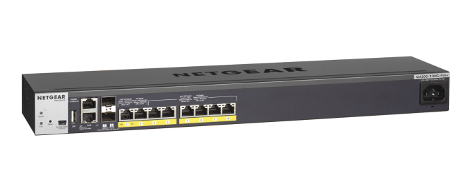 Netgear's M4200-10MG-PoE+ Managed Intelligent Edge Series Switch with 5G/2.5G Switching for High-Speed Wave 2 802.11ac Deployments
The ratification is a big boost for the NBASE-T Alliance. The standardization also lends more credence to the NBASE-T plugfests scheduled to be conducted in October 2016. It will also bring more 2.5G/5GBASE-T products into the market, bring prices down and drive up adoption. The most important aspect is that the existing cabling infrastructure doesn't need a overhaul. This makes it very attractive for business and enterprise users.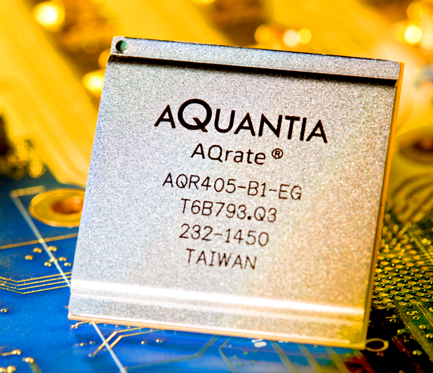 The AQrate Family of NBASE-T PHYs from AQUANTIA - One of the Leading Market Players
From a power user / enthusiast viewpoint, NBASE-T equipment will be a good upgrade. However, readers planning on wiring up their homes would do well to go with Cat 6a cables for future-proofing purposes. 10GBASE-T products (both switches and motherboards / PCIe cards) for enthusiasts are already in the market, thanks to vendors like Asus. NBASE-T adoption will mainly be dictated by business and enterprise users in the near future. As local bandwidth requirements increase in the premises of the average consumer, 2.5G/5GBASE-T will surely find its way into networking gear for traditional consumers also.
More...
-
10-03-16, 10:06 AM #6350
Anandtech: GlobalFoundries Updates Roadmap: 7 nm in 2H 2018, EUV Sooner Than Later?
GlobalFoundries recently announced the first details about its next generation 7 nm manufacturing technology, which is being developed in-house, and revealed plans to start production of chips using the tech in 2018. Initially GlobalFoundries will continue to use deep ultraviolet (DUV) argon fluoride (ArF) excimer lasers with 193 nm wavelength with its 7 nm production process, but over time it hopes to insert extreme ultraviolet lithography (EUV) tools into production flow should their customers need this. Keeping in mind that one of GF’s key customers is AMD, the foundry’s advancements in manufacturing technologies are quite important for the PC market in general.
Tangible Improvements Over 14LPP
GlobalFoundries will use its 7 nm production process to produce high-performance components, such as CPUs, GPUs and SoCs for various applications (mobile, PC, servers, etc.). In general, it means that a number of future products from AMD could be produced using GlobalFoundries’ 7 nm fabrication tech, something we already knew from the wafer supply agreement that the two companies inked earlier this year. Compared to GlobalFoundries’ current leading-edge 14LPP fabrication technology, the initial DUV-only 7 nm process promises over 50% area reduction as well as over 60% power reduction (at the same frequency and complexity) or over 30% performance improvement (at the same power and complexity). In practice, this means that in an ideal scenario GlobalFoundries will be able to double the amount of transistors per chip without increasing its die size while improving its performance per watt characteristics. The company plans to "significantly" re-use equipment and processes it utilizes now for volume production of chips using the 14 nm FinFET technologies for its 7 nm node. Nonetheless, the new process will require an additional multi-billion investment in Fab 8.
As of now, GlobalFoundries has already started to produce test wafers with circuits (IP) from a number of its customers using the 7 nm process in its Fab 8 in Malta, New York. While the company decision to skip 10nm means that it will not be able to use 10nm as a stepping-stone to 7 nm technology, it says that it has gained a lot of experience with FinFETs from the 14LPE and the 14LPP processes. The contract maker of semiconductors expects to finalize specs of its 7 nm technology in the second half of 2017, which implies on start of mass production of commercial chips in the second half of 2018. GlobalFoundries naturally does not reveal timeframes for its 7nm with EUV, but it is safe to say that EUV will be used in 2019 at the earliest.
While GlobalFoundries’ expectations for performance, power, area (PPA) improvements look solid, it should be noted that right now the contract manufacturer is among what's become multiple companies to have confirmed their intentions to pursue a DUV-only 7 nm process technology. DUV in this respect is the tried and true approach, however in order to create 7 nm features it will require using triple/quadruple patterning, which greatly increases design and manufacturing costs as well as cycle times over previous-gen nodes. So while there is a lot of interest in using EUV if it works, many of the major fabs are starting at the same place as GlobalFoundries and at least internally preparing for DUV-only, while hoping EUV will be ready when they want it.
Case in point, Samsung currently hopes to use EUV lithography for critical layers with their 7 nm nodes to avoid triple/quadruple patterning, but are being very careful in how they're wording their plans, saying that they are "reviewing possibilities" of EUV insertion at 7 nm. So it is not cast in stone that Samsung will not proceed with a DUV-only 7 nm if it has to. Meanwhile Intel also once considered to start using EUV for 7 nm. Finally, TSMC does not seem to be afraid of multi-patterning and intends to produce semiconductors using DUV-only 7 nm manufacturing tech in 2H 2018.
It remains to be seen how GlobalFoundries’ and TSMC’s 7 nm processes play out, but keep in mind that the former claims that its 7 nm platform is designed to be “EUV-compatible at key levels”. This means that the company will start using ASML’s TWINSCAN NXE step-and-scan systems for critical layers once they are ready (i.e., their light sources will be powerful enough for mass production and the tools will have more than 80% availability). Since GF's 7 nm with EUV process technology will be used to produce a generation of ICs (integrated circuits) that will follow the initial 7 nm chips, GlobalFoundries makes no secret that the 7 nm with DUV and the 7 nm with EUV are essentially two different process generations (keep in mind that specs of either have not been finalized). Moreover, if EUV is ready for prime time in 2019, GF's 7 nm DUV will be a short-lived node. In fact, GlobalFoundries is already using TWINSCAN NXEs and EUV to speed up prototyping of certain circuits for its clients.
GlobaFoundries Skips 10 nm For Two Reasons
Having announced its 7 nm manufacturing technology, GlobalFoundries confirmed rumors that it decided to skip the 10 nm fabrication process. It looks like there are at least two reasons for this decision and both lie in the PPASC (power, performance, area, schedule and costs) equation. On the one hand, the company figured out that the PPA advantages of its 10 nm technology over its 14LPP process would not be significant. On the other hand, its schedule and costs would further hinder its competitiveness. Now, let’s talk about this in a bit more detailed way.
Since manufacturing technologies are getting more complex, it is not easy to ensure that every new node offers substantial power, performance and area improvements (PPA) over the previous one. As a result, some process technologies are only used by fabless designers of semiconductors for a couple of years, whereas others are used by dozens of companies for many years. GlobalFoundries believes that 10 nm process would not provide tangible performance, power and area advantages over 14LPP process technology (which is based on 20 nm back-end-of-line interconnect flow) and would become a short-lived transitional node, hence their reason to skip it. We have seen a few such nodes in the recent years: as a limited number of firms used 45 nm, 32 and 20 nm process technologies, albeit all for different reasons.
If we take a look at the advertised PPA improvements for the most recent leading-edge process technologies from GF, Samsung and TSMC, it will be clear that transition to 10 nm node will bring improvements to TSMC's abilities, but not by a large enough degree to satisfy all of its customers (we observed something similar with the CLN20SOC several years ago). Moreover, Samsung's numbers are somewhat less impressive (keep in mind that GF's 14LPP was licensed from Samsung), confirming GlobalFoundries expectations.
To a degree, GlobalFoundries seems to be at least partially right in its thinking of 10 nm as of a transitional node. Only three customers have taped out their 10 nm chips at TSMC so far, less than six months before TSMC intends to get its first 10 nm revenue (in Q1 2017). By contrast, tens of companies taped out their 16 nm (CLN16FF) products long before the start of high-volume production in the second half of 2015. What is more important is that according to TSMC, its 10 nm fabrication process will be mostly used by mobile SoC developers (read: Apple, Qualcomm, MediaTek), which desperately need to squeeze more transistors into new chips every year, improve performance and reduce power consumption by a bit too. Such customers are less concerned about manufacturing costs and aggressive improvements, they simply need new technologies to make certain progress due to market demands.Advertised PPA Improvements of Leading Edge Process Technologies
Data announced by companies during conference calls, press briefings and in press releasesGlobalFoundries Samsung TSMC 7nm DUV
vs 14LPP14LPP
vs 28LPP10LPE
vs 14LPP10LPP
vs 10LPE20SOC
vs
28 nm16FF+
vs
28HPM16FF+
vs
20SOC10FF
vs
16FF+7FF
vs
10FFPower >60% 60% 30% none 25% 70% 60% 40% 30% 40% >10% >10% 30% 65% 40% 20% - Area Reduction >50% 50% 32% none 50% >37%
Meanwhile, TSMC’s 7 nm manufacturing technology will be used by multiple customers of the company, including those from high-performance computing space, the company said recently (it does not mean, though, that nobody from HPC space is going to use 10 nm). TSMC plans to start volume production of 7 nm chips in the first half of 2018, so, it is a little bit ahead of GlobalFoundries with this node. However, its first EUV-based process technology (5 nm) is scheduled for 2020, so, the company might be a little behind its rival when it comes to next-gen lithography.
Samsung demonstrated the first wafers processed using its 10LPE (10 nm, low-power early) technology in May, 2015, and disclosed plans to start volume production of chips using its 10 nm tech in late 2016. In addition, the company is planning to quickly roll-out an improved version of the tech called 10LPP, the company said earlier this year. Since Samsung needs to produce leading-edge SoC for its smartphones, it is not surprising that it is also deploying 10 nm fabrication processes: even in case it does not have a lot of foundry customers for them, it is going to need them itself to stay competitive against Apple (and potentially land Apple as a foundry client). Moreover, if Samsung requires EUV for its 7 nm process technology, it will have to use 10 nm before ASML is ready with its commercial EUV step-and-scan systems. In fact, this is why Samsung does not reveal whether it expects to start making chips using 7 nm process in 2019 or later.
Meanwhile, there is another reason why GlobalFoundries decided to skip the 10 nm fabrication technology (in addition to insignificant performance and area advantages over the 14LPP). Back in 2014, the company acquired assets of IBM Microelectronics along with a team of developers. Naturally, the integration of IBM staff took time, so instead of creating a 10 nm manufacturing process (which would be late anyway), the company decided to focus on its 7 nm technology platform. The latter will be the first process developed by the team consisting of GF and IBM developers.
Finally, keep in mind that while makers of semiconductors use terms like 7 nm or 10 nm to name their fabrication technologies, such numbers nowadays do not necessary reflect transistor density and other factors. Not all 10 nm manufacturing technologies are created equal. For example, Intel argues that transistor density of its 10 nm process is going to be comparable to transistor densities of competing 7 nm technologies. Nonetheless, a new node is still a new node with its own advantages compared to its direct, in-house predecessor.
Smooth Transition to EUV
Nowadays both semiconductor makers and manufacturers of production equipment agree that EUV will be required to make chips using smaller fabrication technologies, and the question is whether ASML will be ready with viable tools for 7 nm or for 5 nm nodes. As a result, everyone has to make decisions about when to start using EUV scanners for critical layers.
ASML and Cymer are making a steady progress with their EUV tools and manufacturers of semiconductors are learning how to use those tools. So far, only TSMC has publicly announced plans to use EUV for commercial 5 nm chips in 2020. Samsung has publicly mulled over using EUV tools for its 7 nm semiconductors, but it does not specify when. GlobalFoundries said that it could use EUV for its 7 nm manufacturing technology, but also did not specify exact timing. Intel is still weighing its options, hence, it is still possible that the company will start to use EUV for its 7 nm fabrication process. Meanwhile, SMIC and UMC have not specified their plans concerning next-gen lithography. In fact, both companies yet have to catch up with their rivals when it comes to FinFET first.Leading-Edge Industry Lithography Roadmap, Mass Production
Data announced by companies during conference calls, press briefings and in press releases2016 2017 2018 2019 2020 1H 2H 1H 2H GlobalFoundries 14LPP 7 nm DUV 7nm with EUV
exact timing not announcedIntel 14 nm
14 nm+10 nm no data Samsung 14LPP
14LPC10LPE 10LPP 7LPP (7nm with EUV)
exact timing not announcedSMIC 28 nm 14 nm in development TSMC CLN16FF+ CLN16FFC CLN10FF CLN7FF unknown 5 nm EUV UMC 28 nm 14 nm no data
By developing a 7 nm process technology “compatible with EUV at key levels”, which essentially means two generations of the fabrication process, GlobalFoundries plays it safe:
- Firstly, it will have an all new process technology ready for production in 2H 2018. It is several months later than TSMC, but is still ahead of Intel and such manufacturing tech advantage could be good for AMD as well as other customers of GlobalFoundries (but bear in mind increased costs and cycle times).
- Secondly, once EUV tools are ready for prime time, GlobalFoundries will have a proven and polished-off process technology ready for EUV insertion (keep in mind that 193 nm ArF tools will be used for the majority of layers for a long time).
- Thirdly, even if ASML’s tools are not ready by 2H 2019 (something that its clients will learn well ahead of that timeframe), GlobalFoundries will have a competitive node and time to develop its next process with, or without EUV.
Of course, in certain circumstances GlobalFoundries may end up competing against TSMC’s 5 nm EUV technology with its 7 nm manufacturing process in 2020, but this is something the company is going to try to avoid.
GlobalFoundries to Offer EUV and FD-SOI
GlobalFoundries does not put all eggs in one basket. While companies like TSMC and Samsung develop low-cost/low-power versions of their FinFET manufacturing technologies in a bid to attract smaller players, GF also plans to keep developing new planar fabrication processes featuring FD-SOI. Therefore, for cost effective, low power and radio applications, the company will keep using its 22FDX (it uses back-end-of-line interconnect flow of STMicroelectronics’ 28nm FD-SOI as well as front-end of line of STM’s 14nm FD-SOI process technology) and eventually 12FDX technologies (also announced this month).
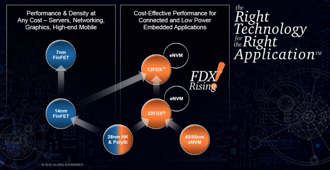
Since it is considerably cheaper to design chips featuring planar transistors, these technologies are going to be used by various smaller fabless semiconductor developers. In general, GlobalFoundries positions its 22FDX as an alternative for 14/16 nm FinFET technologies, whereas the 12FDX is going to compete against 10 nm and, possibly, sub-10 nm processes in 2019 and beyond. Samsung, another FD-SOI backer, plans to add eNVM (embedded non-volatile memory) to its 28FDS platform in 2018, but so far it has not announced any plans for a new FD-SOI technology platform.
It remains to be seen is how successful the FD-SOI offerings from GlobalFoundries will be, given the competition. Nonetheless, GlobalFoundries and Samsung are the only contract makers of semiconductors, which have announced plans to offer both leading-edge FinFET as well as planar FD-SOI manufacturing processes in 2020 and beyond. Moreover, GlobalFoundries is the only company, who disclosed plans for a sub-20 nm FD-SOI fabrication technology.
More...


 Quote
QuoteThread Information
Users Browsing this Thread
There are currently 14 users browsing this thread. (0 members and 14 guests)


Bookmarks