

Results 6,941 to 6,950 of 12091
Thread: Anandtech News
-
05-09-17, 09:47 PM #6941
Anandtech: NVIDIA Announces Earnings for Q1 FY 2018
This afternoon, NVIDIA announced their earnings for the first quarter of their 2018 fiscal year. NVIDIA has been having a lot of success moving their core GPU business away from just PC gaming, and into far more categories, and the earnings today suggest that they’ve made some excellent strategic moves, coupled with solid product launches. Revenue for the quarter came in at $1.94 billion, which is an increase of 48% from Q1 2017. Gross margin was up 1.9% from a year ago, with 59.4% for the quarter. Operating income was up a staggering 126% to $554 million, and net income was up 144% to $507 million. This resulted in earnings per share of $0.79, up 126% from a year ago when they were $0.35. Last year, NVIDIA had record revenues, and this fiscal year they are off to an even better start.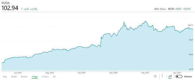
Despite NVIDIA diversifying, and creating new markets for their GPUs, gaming is still the core of the company. They have come a long way in some of their segments, but gaming still accounts for 53% of their revenue, meaning it is larger than every other segment combined. Interestingly, despite the high gains in practically all other segments, the growth in gaming was higher. Last year at the end of Q1 2017, gaming accounted for only 52.6% of their revenue. For this quarter, revenue from gaming was $1.027 billion, compared to $687 million a year ago. A strong year of Pascal under their belt, and the launch of the GeForce GTX 1080 Ti, shows that there’s still room for growth in the PC market.NVIDIA Q1 2018 Financial Results (GAAP) Q1'2018 Q4'2017 Q1'2017 Q/Q Y/Y Revenue (in millions USD) $1937 $2173 $1305 -11% +48% Gross Margin 59.4% 60.0% 57.5% -0.6% +1.9% Operating Income (in millions USD) $554 $733 $245 -24% +126% Net Income $507 $655 $208 -23% +144% EPS $0.79 $0.99 $0.35 -20% +126%
Professional Visualization, which is the segment for Quadro, had much lower growth than GeForce, but still increased revenues from $189 million a year ago, to $205 million today. That’s reasonable growth of 8.4%, but compared to pretty much every other NVIDIA segment, it seems like it’s not growing at all.
Datacenter is where NVIDIA has really found a great home for their GPU business, especially with the growth in machine learning and AI. NVIDIA’s Tesla business was once an afterthought for the company (well, maybe not the company, but outsiders looking in), but with the launch of the Tesla P100 and smaller variants, and DGX-1, NVIDIA has found some big customers for their datacenter compute products, including Microsoft, Google, and several other cloud vendors. Datacenter revenue was up 186% to $409 million. To put that in perspective, NVIDIA didn’t even discuss datacenter revenues even two years ago, and it’s now their second largest business. Not only that, it’s very likely one of their highest margin businesses as well.
Automotive, which came out of the failed Tegra smartphone and tablet business, is still showing strong growth as well. There’s a great saying about making lemonade, and NVIDIA has certainly done that. Revenue for this segment was up almost 24% to $140 million for the quarter.
Finally, OEM and IP is the only segment to have a falling quarter, with revenues down about 10% to $156 million.
NVIDIA has followed up strong product launches with solid diversification of their core business, and the results speak for themselves. The last couple of years have been very strong, and it appears that growth is going to continue for at least the near term. NVIDIA is expecting revenues for next quarter to be $1.95 billion, plus or minus 2%, with a gross margin of 58.4% plus or minus 0.5%.NVIDIA Quarterly Revenue Comparison (GAAP) In millions Q1'2018 Q4'2017 Q1'2017 Q/Q Y/Y Gaming $1027 $1348 $687 -23.8% +49.5% Professional Visualization $205 $225 $189 -8.9% +8.5% Datacenter $409 $296 $143 +38.2% +186% Automotive $140 $113 $93 +23.9% +50.5% OEM & IP $156 $176 $173 -11.4 -9.8%
Source: NVIDIA Investor Relations
More...
-
05-10-17, 11:17 AM #6942
Anandtech: The NVIDIA GPU Tech Conference 2017 Keynote Live Blog
Taking place today is NVIDIA's keynote for GTC 2017. This keynote provides an annual, high-level overview of what NVIDIA is planning over the next couple of years. And with any luck, we may see something on the forthcoming Volta architecture as well.
More...
-
05-10-17, 11:17 AM #6943
Anandtech: Imagination Announces PowerVR Series 8XT GT8525: Their First Furian GPU De
Back in March of this year, Imagination announced their next-generation GPU architecture: Furian. Their first new architecture since Rogue in 2010, Furian iterates off of what Imagination has learned in the intervening years to further improve their architecture’s performance, power efficiency, and die area efficiency. At the time the company only announced the architecture and not any GPU designs based off of it, but today they are taking the wraps off of the first Furian design: the PowerVR Series 8XT GT8525.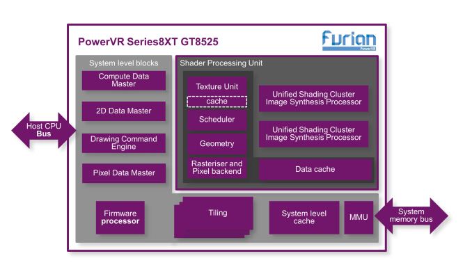
With their first design, Imagination is taking the pragmatic route – or as they like to put it, the balanced route. Outside of Apple, most of Imagination’s customers have been licensing two cluster designs from the high-performance PowerVR families (6XT, 7XT, 7XT+), so this is where Imagination is starting for Furian and the new Series 8XT.
By and large then, the GT8525 is exactly what you’d expect for a 2 cluster design based on Imagination’s earlier disclosure. 2 clusters are by design intended to fit inside of one of Imagination’s shader processing units, giving the design a single such unit.
The significance of this choice, besides being the smallest possible full implementation of Furian (before you start removing pieces from the design and get fractional) is that one of the areas Imagination focused on was improving the pixel and texel throughput at this level. As a result, a 2 cluster Furian design offers 8 pixels and 8 bilinear filtered texels per clock whereas a 2 cluster Rogue (e.g. GT7200) offered 4 of each. So even though it’s still only 2 clusters, even after you ignore the architectural improvements, there’s actually a lot more hardware working in a 2 cluster design.
By the numbers, Imagination is touting some rather significant performance improvements for GT8525 over its predecessor, GT7200. 50% faster performance in GFXBench Manhattan, 80% faster in GFXBench T-Rex, 50% more (on paper) FLOPS, etc. All of this would be at equal clockspeeds, though the company isn’t talking about power consumption or die size right now, so it’s hard to get a feel for where energy and area efficiency of the new design stands.PowerVR GPU Comparison GT8525 GT7200 Plus Clusters 2 2 FP32 FLOPS/Clock 192
(128 MAD + 64 MUL)128
(MAD)FP16 Ratio 2:1 (Vec2) 2:1 (Vec2) Pixels/Clock (ROPs) 8 4 Texels/Clock 8 4 APIs OpenGL ES 3.2 + Vulkan OpenGL ES 3.2 + Vulkan OpenCL 2.x 2.0 Architecture Furian Rogue
With this 2 cluster design, Imagination is going to be pursuing a mix of markets, though ultimately it’s up to SoC venders to build suitable SoCs. This includes smartphones, of course, but also mobile VR, which is a growing market that has a lot of potential for GPU vendors like Imagination given the performance requirements. The company is also pitching the new GPU design for the automotive market, where along with infotainment duties, a 2 cluster design should be powerful enough for some light ADAS work (presumably just doing computer vision on one or two camera streams).
To that end, the company has also announced that the design has already been delivered to their (unnamed) lead customer. Traditionally this would be Apple, but of course we know that Apple will be rolling out their own GPU architecture starting in the next 1-2 years. Instead this could be the likes of MediaTek or another at-large SoC vendor. In any case it’s possible we’ll see the devices using this design in 2018, though it’s ultimately up to the SoC vendor and device vendor on how quickly they want to move.
More broadly speaking, Furian and the GT8525 will be a critical product for Imagination. As the company announced last week, they are doubling-down on their GPU products and selling off everything else. Without Apple, they need to capture a larger part of the GPU market share in smartphones and other embedded devices. Consequently, starting with a 2 cluster design is the smart choice here, as 2 cluster designs are going to have the highest volume.
More...
-
05-10-17, 12:30 PM #6944
Anandtech: BIOSTAR Reveals Two AMD AM4 Crypto Mining Motherboards
Although largely overshadowed by more efficient ASIC rigs, there are still people using GPUs to accumulate digital currencies and/or create cheap OpenCL based systems. It is with those users in mind that BIOSTAR has now expanded their lineup of specialized cryptocurrency mining motherboards to include two new AMD AM4 models.
Referred to as the TA320-BTC and TB350-BTC, these are the first AM4-based crypto mining motherboards announced, and as such make BIOSTAR the only manufacturer to offer mining motherboards for both mainstream platforms. This following the recent launch of Biostar's Intel LGA1151-based TB250-BTC model.
Gallery: BIOSTAR TB350-BTC


As you might have surmised, the TA320-BTC is based on the lower-end AMD A320 chipset, while the TB350-BTC is based on the mid-range AMD B350 chipset. After carefully scrutinizing the specifications list of both models, the only difference that we could find – chipset aside – is that the A320-based model is limited to memory speeds of DDR4-2666, while the B350 model supports up to DDR4-3200. These models only have two DDR4 memory slots each, so they are limited to 32GB of system memory.
Both motherboards support AMD's latest Ryzen processors (up to 95W TDP) and the upcoming 7th Generation A-Series APUs, which should be no problem for the 7-phase power design. Given their specialized purpose, these motherboards only have four SATA 6Gb/s ports and no M.2 slots. USB connectivity is quite decent with six USB 3.1 Gen1 ports (four rear, one header) and six USB 2.0 ports (four rear, one header). Two of the USB 2.0 ports are high amperage capable, so they can handle water pumps and/or fans that require up to 1.5 amps. Networking duties are handled by one gigabit LAN port that is powered by a Realtek RTL8111H controller. In terms of rear I/O connectivity, aside from the aforementioned ports, there are two legacy PS/2 connectors, a single DVI-D video output, and three audio jacks courtesy of a low-end Realtek ALC887 codec.
The key selling point of these two models is obviously their six PCIe slots. They each have one PCIe 3.0 x16 slot, two PCIe 3.0 x1 slots, and three PCIe 2.0 x1 slots. The PCIe x16 slot will operate at x8 if an APU is installed, due to AM4 APU limitations. Now you may be asking how PCIe x1 slots are useful when it comes to handling multiple graphics cards, and the answer is that miners use PCIe 1x to x16 riser cards with flexible extender cables (not included) and special cases that hold the graphics cards well above the motherboard. Crucially, there are also two 4-pin Molex power connectors intended to bolster power delivery to the PCIe slots, and they must be used when mining due to the increased power demands.
While full-size ATX motherboards generally measure 305mm × 244mm, these two models are both slightly shorter and narrower than the ATX standard at 295mm x 210mm. That may cause issues with certain cases, but BIOSTAR is likely betting on the fact that those who purchase these motherboards will be installing them on purpose-built open test benches.
We have no information with regard to pricing or availability, but both models will have a 3-year warranty in applicable regions. We expect the pricing to be quite low, given the margins that miners typically work with. Mining aside, any non-PCIe bandwidth limited task for compute, using OpenCL / CUDA and such could also be used.
Gallery: BIOSTAR TA320-BTC


Related Reading- ASRock Launch H81 Pro BTC for Cryptocurrency Mining
- The Rush to Bitcoin ASICs: Ravi Iyengar launches CoinTerra
More...
-
05-10-17, 04:43 PM #6945
Anandtech: NVIDIA Volta Unveiled: GV100 GPU and Tesla V100 Accelerator Announced
Today at their annual GPU Technology Conference keynote, NVIDIA CEO Jen-Hsun Huang announced NVIDIA’s first Volta GPU and Volta products. Taking aim at the very high end of the compute market with their first products, NVIDIA has laid out a very aggressive technology delivery schedule in order to bring about another major leap in GPU deep learning performance.
As a quick history lesson, NVIDIA first unveiled the Volta architecture name all the way back in 2013. What eventually happened with their architectures wasn’t what was originally announced – Maxwell and Volta became Maxwell, Pascal, and Volta – but Volta is the last GPU architecture on NVIDIA’s current public roadmap. Until now, all we’ve known about Volta is that it existed; NVIDIA has opted to focus on what’s directly in front of them (e.g. Pascal), one generation at a time.
So let’s talk Volta. For their first Volta products, NVIDIA is following a very similar path as they did with Pascal last year. Which is to say that they are kicking off their public campaign and product stack with a focus on business, HPC, and deep learning, rather than consumer GPUs. Volta is a full GPU architecture for both compute and graphics, but today’s announcements are all about the former. So the features unveiled today and as part of the first Volta GPU are all compute-centric.
NVIDIA’s first Volta GPU then is the aptly named GV100. The successor to the Pascal GP100, this is NVIDIA’s flagship GPU for compute, designed to drive the next generation of Tesla products.
By the numbers, the GV100 is something I can honestly say is a audacious GPU, an adjective I’ve never had a need to attach to any other GPU in the last 10 years. In terms of die size and transistor count, NVIDIA is genuinely building the biggest GPU they can get away with: 21 billion transistors, at a massive 815mm2, built on TSMC’s still green 12nm “FFN” process (the ‘n’ stands for NVIDIA; it’s a customized higher perf version of 12nm for NVIDIA).NVIDIA GPU Specification Comparison GV100 GP100 GK110 CUDA Cores 5376 3840 2880 Tensor Cores 672 N/A N/A SMs 84 60 15 CUDA Cores/SM 64 64 192 Tensor Cores/SM 8 N/A N/A Texture Units 336 240 240 Memory HBM2 HBM2 GDDR5 Memory Bus Width 4096-bit 4096-bit 384-bit Shared Memory 128KB, Configurable 24KB L1, 64KB Shared 48KB L2 Cache 6MB 4MB 1.5MB Half Precision 2:1 (Vec2) 2:1 (Vec2) 1:1 Double Precision 1:2 1:2 1:3 Die Size 815mm2 610mm2 552mm2 Transistor Count 21.1B 15.3B 7.1B TDP 300W 300W 235W Manufacturing Process TSMC 12nm FFN TSMC 16nm FinFET TSMC 28nm Architecture Volta Pascal Kepler
To put this in perspective, NVIDIA’s previous record holder for GPU size was GP100 at 610mm2. So GV100, besides being on a newer generation process, is a full 33% larger. In fact NVIDIA has gone right to the reticle size of TSMC’s process; GV100 is as big a GPU as the fab can build. Now NVIDIA is not a stranger with reticle sizes, as GM200 happened to do the same thing with TSMC’s 28nm process, but at only 601mm2, GV100 is much larger still.
Now why the focus on die size first and foremost? At a high level, die size correlates well with performance. But more significantly, this is a very visible flag about how NVIDIA is pushing the envelope. The company is not discussing chip yields at this time, but such a large chip is going to yield very poorly, especially on the new 12nm FFN process. NVIDIA is going to be sacrificing a lot of silicon for a relatively small number of good chips, just so that they can sell them to eager customers who are going to pay better than $15K/chip. This is how badly NVIDIA’s customers want more powerful GPUs, and how hard NVIDIA is going to push the limits of modern fab technology to deliver it.
The chip’s absurd size aside, GV100 promises to be powerful. The chip contains 84 SMs – as this is a compute product, each SM is 64 CUDA cores in size – making for a total of 5376 FP32 CUDA cores. Joining those FP32 cores are 2688 FP64 CUDA cores (meaning NV is maintaining their 1:2 FP64 ratio), but also a new core that NVIDIA is calling the Tensor Core.
Tensor Cores are a new type of core for Volta that can, at a high level, be thought of as a more rigid, less flexible (but still programmable) core geared specifically for Tensor deep learning operations. These cores are essentially a mass collection of ALUs for performing 4x4 Matrix operations; specifically a fused multiply add (A*B+C), multiplying two 4x4 FP16 matrices together, and then adding that result to an FP16 or FP32 4x4 matrix to generate a final 4x4 FP32 matrix.
The significance of these cores are that by performing a massive matrix-matrix multiplication operation in one unit, NVIDIA can achieve a much higher number of FLOPS for this one operation. A single Tensor Core performs the equivalent of 64 FLOPS per clock, and with 8 such cores per SM, 1024 FLOPS per clock per SM. By comparison, even with pure FP16 operations, the standard CUDA cores in an SM only generate 256 FLOPS per clock. So in scenarios where these cores can be used, NV is slated to be able to deliver 4x the performance versus Pascal.
Now there are a bunch of unknowns here, including how flexible these cores are, and how much die space that they take up versus FP32 CUDA cores. But at a high level, this is looking like a relatively rigid core, which would make it very die-space efficient. By lumping together so many ALUs within a single core and without duplicating their control logic or other supporting hardware, the percentage of transistors in a core dedicated to ALUs is higher than on a standard CUDA core. The cost is flexibility, as the hardware to enable flexibility takes up space. So this is a very conscious tradeoff on NVIDIA’s part between flexibility and total throughput.
Continuing down the spec list, each SM contains 4 texture units, the same number as with the GP100. Joining those texture units is yet another rework of NVIDIA’s L1 cache/shared memory architecture. Whereas GP100 had a 24KB L1/Texture cache and 64KB shared memory per SM, on GV100 it’s now a 128KB of L1 data cache/shared memory per SM, with the precise L1/shared memory split being configurable. Besides unifying these caches, this means there’s more cache/memory overall, 40KB more per SM. On the other hand, the register file remains unchanged at 256KB of registers (4x16K 32-bit registers) per SM.
At a higher level, the 84 SMs are organized 2 to a TPC, just as with GP100, giving us a 42 TPC count. These TPCs are in turn organized 7 to a GPC, and then 6 GPCs. Feeding the beast is once again HBM2, with NVIDIA using 4 stacks of it like GP100. It’s interesting to note here that while memory clocks have only increased by 25% for the respective Tesla SKUs, NVIDIA is claiming a 50% increase in effective memory bandwidth due to a combination of that and better memory efficiency. Meanwhile the L2 cache system between the memory and GPCs has also been enhanced; there’s now 768KB of L2 cache per ROP/memory partition, versus 512KB on GP100. This means L2 cache for the whole chip now stands at 6MB.
Going to a higher level still, Volta also implements a newer version of NVLink. This is the previously announced NVLink 2, and along with greater link bandwidth – up from 20GB/sec bidirectional to 25GB/sec bidirectional – there are now 6 NVLinks per GPU for GV100, 2 more than on GP100. Critically, NVLInk 2 also introduces cache coherency allowing the GPUs to be cache coherent with CPUs. Expect to see this play a big part in the eventual Power 9 + Volta systems.
Finally, while the full details on this will have to wait until later, NVIDIA has also unveiled that they’ve made a pretty significant change to how SIMT works for Volta. The individual CUDA cores within a 32-thread warp now have a limited degree of autonomy; threads can now be synchronized at a fine-grain level, and while the SIMT paradigm is still alive and well, it means greater overall efficiency. Importantly, individual threads can now yield, and then be rescheduled together. This also means that a limited amount of scheduling hardware is back in NV’s GPUs.
Overall, GV100 is a 3 billion dollar R&D project for NVIDIA, their largest project to date for their largest GPU to date. NV is expecting the first GV100 products to start shipping in Q3 of this year and they won’t be cheap – on the order of $18K per GPU for a DGX system – however for those customers with deep pockets and who will essentially pay NVIDIA to eat the risk of producing such a large GPU, this will be the most powerful GPU released yet.
Tesla V100
The first product to use the GV100 GPU is in turn the aptly named Tesla V100. Like its P100 predecessor, this is a not-quite-fully-enabled GV100 configuration. Overall, only 80 of 84 SMs are enabled for yield reasons.
By the numbers, Tesla V100 is slated to provide 15 TFLOPS of FP32 performance, 30 TFLOPS FP16, 7.5 TFLOPS FP64, and a whopping 120 TFLOPS of dedicated Tensor operations. With a peak clockspeed of 1455MHz, this marks a 42% increase in theoretical FLOPS for the CUDA cores at all size. Whereas coming from Pascal, for Tensor operations the gains will be closer to 6-12x, depending on the operation precision.NVIDIA Tesla Family Specification Comparison Tesla V100 Tesla P100 Tesla K40 Tesla M40 Stream Processors 5120 3584 2880 3072 Core Clock ? 1328MHz 745MHz 948MHz Boost Clock(s) 1455MHz 1480MHz 810MHz, 875MHz 1114MHz Memory Clock 1.75Gbps HBM2 1.4Gbps HBM2 6Gbps GDDR5 6Gbps GDDR5 Memory Bus Width 4096-bit 4096-bit 384-bit 384-bit Memory Bandwidth 900GB/sec 720GB/sec 288GB/sec 288GB/sec VRAM 16GB 16GB 12GB 12GB Half Precision 30 TFLOPS 21.2 TFLOPS 4.29 TFLOPS 6.8 TFLOPS Single Precision 15 TFLOPS 10.6 TFLOPS 4.29 TFLOPS 6.8 TFLOPS Double Precision 8.5 TFLOPS
(1/2 rate)5.3 TFLOPS
(1/2 rate)1.43 TFLOPS
(1/3 rate)213 GFLOPS
(1/32 rate)GPU GV100
(815mm2)GP100
(610mm2)GK110B GM200 Transistor Count 21B 15.3B 7.1B 8B TDP 300W 300W 235W 250W Cooling N/A N/A Active/Passive Passive Manufacturing Process TSMC 12nm FFN TSMC 16nm FinFET TSMC 28nm TSMC 28nm Architecture Volta Pascal Kepler Maxwell 2
The Tesla V100 will be paired with 16GB of HBM2. At this time no one is producing an 8-Hi HBM2 stack, so NVIDIA cannot expand their memory capacity at 4 stacks. However the memory clockspeed has improved by 25% over Tesla P100, from 1.4Gbps to 1.75Gbps.
Also like the Tesla P100, NVIDIA is using a mezzanine card. They have not shown the new connector – expect it to have more pins to account for the additional NVLinks – but the overall size is similar. NVIDIA calls this the SXM2 form factor.
In terms of power consumption, Tesla V100 will have a TDP of 300W, like its predecessor. NVIDIA notes that power efficiency of V100 is higher than P100, though it will be interesting to see just where this stands, and how often the card actually power throttles.
The first product to ship with Tesla V100 will be the NVIDIA DGX-1V, the Volta version of their DGX server. Similar to their Pascal launch, starting with DGX sales allows NVIDIA to sell 8 GPUs in one go, and for a premium at that. A DGX-1V will set you back a cool $149,000. The payoff? It ships in Q3, whereas OEM P100 designs won’t be available until Q4.
Gallery: NVIDIA Volta Unveiled: GV100 GPU and Tesla V100 Accelerator Announced


More...
-
05-10-17, 07:29 PM #6946
Anandtech: AT20 Giveaway Day 11.5: Corsair Has the Power (And Memory Too!)
Taking us into our afternoon giveaway for this Wednesday is Corsair. The company, which provides a smorgasbord of PC components ranging from DRAM to peripherals to pre-built PCs, likes to pride themselves on their high-end components. So I’m sure everyone will be eager to win in today’s giveaway, as the company has sent over some of their best DRAM and a PSU.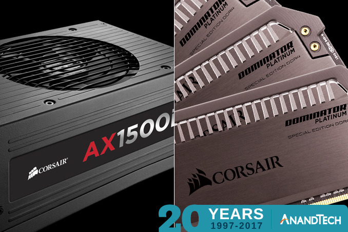
For DRAM, the company has given us a Dominator Platinum Special Edition 32GB (4x8GB) kit in chrome, a kit so rare that they’re individually numbered. Meanwhile on the power supply front, the company is providing their immensely powerful 1500 Watt (!) AX1500i fully modular PSU, along with a premium sleeved cable kit to complete the package.
- Corsair Dominator Platinum Special Edition DDR4 32GB (4x8GB) Kit, Chrome
- Corsair AX1500i PSU & Premium Sleeved Cable Kit
The AnandTech 20th Anniversary Celebration – Corsair Giveaway
Corsair Dominator Platinum Special Edition DDR4 32GB (4x8GB) KitThe first item on our list is Corsair’s flagship-level memory kit, the Dominator Platinum SE. This is a 32GB (4x8GB) kit, which runs at DDR4-3200 speeds with 14-16-16 timings, and a voltage of 1.35v. The company advertises the RAM of being able to be further overclocked to DDR4-3600 speeds, if DDR4-3200 isn’t enough.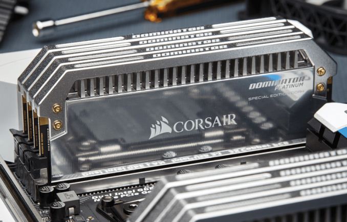
Besides being the company’s fastest memory, the Dominator Platinum is also among their rarest. The company only makes 500 kits of a given configuration and color – to the point where they individually number the kits. The DIMMs themselves feature a sizable aluminum heatspreader (in this case colored chrome) along with a white LED light bar to make the DIMMs quite literally shine.
Corsair AX1500i PSU w/Premium Sleeved CablesOur second prize of the day is Corsair’s flagship power supply, the AX1500i. This massive 1500 Watt fully modular PSU is designed to be the last word in power supplies, and is capable of powering virtually almost any system that can actually be built. In fact it’s so powerful that to actually get 1500 Watts sustained, it needs a 15A+ circuit that runs at 115V, which is to say that it requires a properly wired outlet and most of a circuit to itself.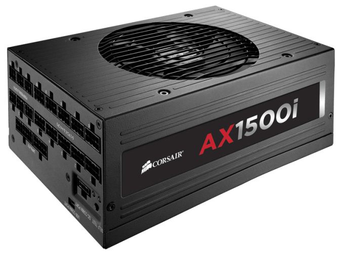
Yet despite being ludicrously powerful, the PSU is also surprisingly efficient, reaching the 80Plus Titanium threshold. As a result, the powerful PSU doesn’t waste a lot of power even when idling, which can be difficult for high-power PSUs. As our own E. Fylladitakis noted back in his review of this PSU “Corsair has simply tried to create the very best power supply possible, regardless of the cost and market potential. They did succeed on breaking almost every performance record we can come up with for a consumer-grade PSU”.
Rounding out the package, Corsair is also throwing in a set of their premium sleeved PSU cables. While the AX1500i already comes with cables, Corsair’s optional cables take things one step further with in-line capacitor and a paracord mesh braiding around the cables.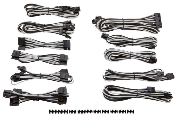
Finally, as with our other giveaways, today’s giveaway is only open for 48 hours, so be sure to enter soon. However please note that for legal reasons, we’re only able to open these giveaways to residents of the United States.
Good luck to everyone! And be sure to check in tomorrow for our next giveaway.
Gallery: AT20 Giveaway Day 11.5: Corsair Has the Power (And Memory Too!)


More...
-
05-11-17, 08:12 AM #6947
Anandtech: AT20 Giveaway Day 12: Patriot Brings out the Red, Green, and Blue with RAM
Today we’re kicking things off with day 12 of our 20 day giveaway celebration of AnandTech’s 20th anniversary.
This morning we have prizes from the pleasant people over at Patriot. The memory, flash storage, and peripherals vendor has sent over a mix of their gear, including both DDR4 RAM and some of their latest peripherals. For RAM we have a 16GB kit of their Viper Elite DDR4-2400. Meanwhile for peripherals the company has brought out the Red, Green, and Blue, with their RGB-equipped Viper V370 headset, Viper V570 mouse, and Viper V760 keyboard.
- Viper Elite Series DDR4-2400 16GB (2x8GB), Blue
- Viper V370 RGB 7.1 Virtual Surround Gaming Headset
- Viper V570 RGB Laser Gaming Mouse
- Viper V760 Gaming Mechanical Keyboard
The AnandTech 20th Anniversary Celebration – Patriot Memory Giveaway
Viper Elite Series DDR4-2400 16GB (2x8GB)Patriot originally got their start in memory, so that too is where we’ll start. The Viper Elite Series kit we’re giving away is a 16GB (2x8GB) set of DIMMs that run at DDR4-2400 with 15-15-15 timings. This is the highest speed grade that DDR4 supports without overclocking, and consequently the kit operates at a cool 1.2v. Meanwhile a blue heatshield ensures that the DIMM is protected, and what little heat is generated is easily dissipated.
Viper V370 RGB Gaming HeadsetOur second prize of the day is the Viper V370 RGB 7.1 Virtual Surround Gaming Headset. This closed-back audio headset features a pair of 40mm drivers and an additional set of 30mm drivers for bass, along with a built-in microphone. And living up to its name, it also includes RGB lighting built into the headset.
Viper V570 RGB Laser Gaming MouseOur third prize is the Viper V570 Laser Gaming Mouse. This right-handed mouse uses a laser sensor that goes up to 3200 DPI, while also offering an adjustable weight and 13 additional macro buttons. Rounding out the package, the mouse also features 7 zones of RGB LED lights.
Viper V760 RGB Gaming Mechanical KeyboardThe final product in today’s giveaway is the company’s Viper V760 RGB Gaming Mechanical Keyboard. Patriot’s sole keyboard, the V760 uses Kailh’s brown mechanical switches to give the keyboard a tactile feel. The board doesn’t feature any extra keys beyond its base 104 keys, but it does offer extensive macro programming and lighting control through the use of a Function modifier key. And of course, like the other RGB peripherals in Patriot’s collection, the V760 features RGB lighting, thanks to the including of per-key RGB LEDs.
Finally, as with our other giveaways, today’s giveaway is only open for 48 hours, so be sure to enter soon. However please note that for legal reasons, we’re only able to open these giveaways to residents of the United States.
Good luck to everyone! And be sure to check in this afternoon for our next giveaway.
Gallery: AT20 Giveaway Day 12: Patriot Brings out the Red, Green, and Blue with RAM and Peripherals


More...
-
05-11-17, 10:05 AM #6948
Anandtech: Inno3D Debuts Single Slot GeForce GTX 1050 Ti
Inno3D has added a new NVIDIA GeForce GTX 1050 Ti-based video card to its lineup. The Inno3D GeForce GTX 1050 Ti (1-Slot Edition) graphics adapter uses a single-slot cooling system and is designed to tightly packed PCs where space is at a premium.
While small form-factor PCs are on the rise today, single-slot consumer graphics adapters are hard to find. This is partly because the popularity of entry-level discrete video cards is decreasing, and partly because virtually all desktops have enough space for dual-slot AIBs. In the recent months, almost a year after the launch of 14nm/16nm GPUs, the situation began to change. ELSA, Palit Microsystems and XFX have released single-slot graphics cards based on NVIDIA’s GP107, GP104 as well as AMD’s Polaris 11 GPUs. It looks like Inno3D is the fourth company and will now offer a gaming-grade graphics board with a single-slot cooler.
The Inno3D GeForce GTX 1050 Ti (1-Slot Edition) is based on the NVIDIA’s GP107 graphics processor in its full configuration (768 stream processors, 48 texture units, 32 ROPs, 128-bit memory controller, etc.). The graphics adapter runs at clock rates recommended by NVIDIA (1290/1392 MHz base/boost) and is equipped with 4 GB of GDDR5 memory operating at 7000 MT/s. Since the single-slot video card is designed for PCs with reduced power consumption, the model from Inno3D comes without an auxiliary PCIe power connector and does not consume more than 75 W of power.
The single-slot graphics card from Inno3D uses an NVIDIA-branded PCB, just like a similar graphics board from ELSA introduced earlier this year. This may indicate that both ELSA and Inno3D either use PCBs made by an NVIDIA-approved manufacturer, or simply get the boards from the GPU developer itself. In either case, this means that other suppliers of video cards may release similar products eventually.
The single-slot cooling system from Inno3D is made of aluminum, and comes in at 99.8 mm in height and is 211 mm long (so, the card itself is relatively short), as for outputs, the board comes with a dual-link DVD-D, one HDMI 2.0b and one DisplayPort 1.4 header. The AIB supports HDCP 2.2, so it can playback protected content.
The Inno3D GeForce GTX 1050 Ti (1-Slot Edition) is already listed on the company’s website, so expect it to hit the market shortly. The company does not publish its MSRP, but we would expect the price to be close to NVIDIA’s recommendations.
Related Reading:
- XFX Starts to Sell Single-Slot Mini-ITX Radeon RX 460 Slim Graphics Cards
- ELSA Launches a Single-Slot GeForce GTX 1050 Ti 4 GB SP
- GALAX and KFA2 Katana: Single-Slot GTX 1070 GPUs Coming Soon
More...
-
05-11-17, 12:46 PM #6949
Anandtech: Intels Itanium Takes One Last Breath: Itanium 9700 Series CPUs Released
One of Intel’s ventures into the historic mainframe space was Itanium: a 64-bit capable processor designed in conjunction with Hewlett Packard. The main reason for Itanium was to run HP-UX and compete against big names, such as Oracle, using a new IA-64 instruction set. The appeal for the original Itanium parts was support for RAS features, ECC, and cores focus on a wide, parallel architecture - the latest cores support 12-wide execution for example. For a short while, there was success: HP’s systems based on Itanium are advertised as high-uptime mission critical servers, and a number of customers cling to these systems like a child clings to their favorite blanket due to the way they are integrated at the core of the company. The main purpose was to compete against other mission critical servers and mainframes based on SPARC and IBM Power.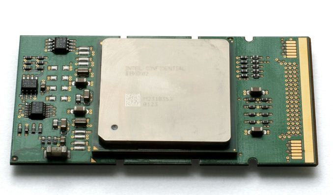
So when the processors were initially delivered to customers, there was potential. However the initial impression was not great - they consumed too much power, were noisy, and needed over the top cooling. Over the years and generations of Itanium, the march into the x86 enterprise space with x86-64 drew potential Itanium customers away, then followed the drop of Microsoft's support for Itanium in 2008, and Oracle's dropped support in 2011. Xeon offerings were becoming popular, with CPUs incorporating the RAS/ECC features required, and Intel decided to slow down Itanium development as a result. In the meantime, due to the way the market was moving, HP transitioned a good part of its product stack to Xeons. Despite this, legal battles between HP and Oracle ensued given predicted support for HP-UX customers. At this point, there were fewer potential Itanium customers each quarter, although existing customers required support.
Today marks the release of the final known variant of Itanium, the 9700 series, beyond assurance testing. Intel spoke to IDG, stating that this generation, code-named Kittson, would be the final member of the Itanium family. These chips are likely to only end up in HP-based Integrity i6 high-uptime servers running HP-UX, and start at $14500. Hewlett Packard Enterprise has stated previously that it will keep support for Itanium-based products until 2025, with the latest OS update (HP-UX 11i v3 2017) coming in June.
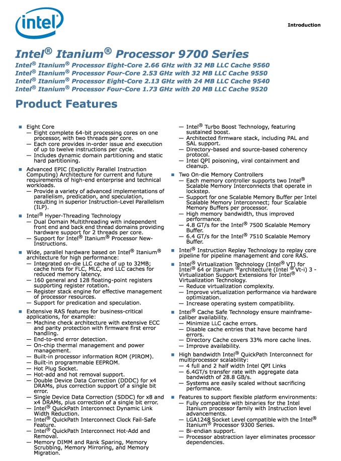
As for the processors themselves, four 9700 processors form the stack, with quad-core and eight-core parts all with hyperthreading, differing in frequency, power, and L3 cache.
*Cost is listed for the equivalent Poulson CPUs.Intel Itanium (Kittson) CPUs Cores/
ThreadsBase
FreqL3 TDP Cost* Itanium 9760 8/16 2.66 GHz 32 MB 170 W $4650 Itanium 9750 4/8 2.53 GHz 32MB 170W $3750 Itanium 9740 8/16 2.13 GHz 24 MB 170 W $2650 Itanium 9720 4/8 1.73 GHz 20 MB 130 W $1350
The base silicon comes in at 3.1 billion transistors, and are made on Intel’s 32nm process. Memory is supported up to DDR3-1067, with two memory controllers but support for scalable memory buffers is present. This is similar to the 9500 series, code-named Paulson. These chips are designed to be purely a drop into previous systems. Intel isn’t announcing an official press release around this, and unlike other ‘new architectures’, there are next to zero improvements. According to the documents, the only change is that the top two SKUs get a clock bump:
There’s probably something new under the hood, perhaps for a specific end-customer, but at this time Intel is directing anything 9700 related to equate to the 9500 series. Customers still interested in Itanium are directed to HPE resellers.
Carousel Image from Konstantin Lanzet (Wikipedia) of Itanium 2 (Poulson)
News Source: IDG
More...
-
05-11-17, 01:34 PM #6950
Anandtech: AT20 Giveaway Day 12.5: Antec Cubes and Powers Your Next Mini-ITX PC
For our final afternoon giveaway of the week, the crew from Antec is looking to give your next computer build a new home. The centerpiece of today’s prize is an Antec Cube (Designed by Razer) Mini-ITX case, the company’s flagship small form factor case. Meanwhile to help power the Cube and its contents, the company is also kicking in one of their 650 Watt Edge power supplies._575px.jpg)
- Antec Cube (Designed by Razer) Mini-ITX Case & Antec Edge 650W PSU
The AnandTech 20th Anniversary Celebration – Antec Giveaway
Antec Cube (Designed by Razer) Mini-ITX CaseStarting things off, at the heart of today’s prize pack is Antec’s latest Cube Mini-ITX case. The case, designed by Razer and literally branded as such, is 14.4 inches tall and features a swept angle design that makes the case more of a parallelepiped (3D parallelogram) than a traditional box case. A case meant o be seen, the top and both sides feature acrylic windows, and Razer-green LED lighting is installed in various points of the case.
Internally, the Cube can take a mini-ITX board, but features enough space for a full length graphics card, or even radiators up to 240mm in size. The case comes with one rear 120mm fan pre-installed, with room for more fans (or the aforementioned radiator) in the front. Meanwhile the PSU receives its own compartment, while the drive bays – supporting 1 3.5 inch drive and up to 4 2.5 inch drives – are on the back side of the case.
Antec Edge 650W PSUIn order to power the Cube, Antec has also sent along one of their Edge-series 650 Watt power supplies. The Edge is a fully modular PSU – ATX power cable and all – sporting a number of different connector options. On the power delivery side, the PSU can deliver 648W over its two 12v rails, and at 80Plus Gold efficiency levels. Finally the PSU sports white LED lighting, which is built into its 135mm fan.
Finally, as with our other giveaways, today’s giveaway is only open for 48 hours, so be sure to enter soon. However please note that for legal reasons, we’re only able to open these giveaways to residents of the United States.
Good luck to everyone! And be sure to check in tomorrow for our next giveaway.
More...


 Quote
QuoteThread Information
Users Browsing this Thread
There are currently 15 users browsing this thread. (0 members and 15 guests)


Bookmarks