

Results 7,131 to 7,140 of 12089
Thread: Anandtech News
-
07-03-17, 09:51 AM #7131
Anandtech: ASUS Launches XG-C100C 10 GBase-T Adapter: Aquantia AQC107, $99
ASUS this week released the first inexpensive vendor-based consumer-grade 10 GbE / 10GBase-T card powered by an Aquantia silicon. The card can be installed in any modern PC with a PCIe 3.0 x4 slot free (either CPU or chipset), and supports 10 Gbps, 5 Gbps, 2.5 Gbps, 1 Gbps and 100 Mbps networking standards over RJ45 connectors using Cat5e/Cat6 cabling. What is important is that the board costs less than $100, at a lower price than Aquantia quoted in the initial announcement ($127).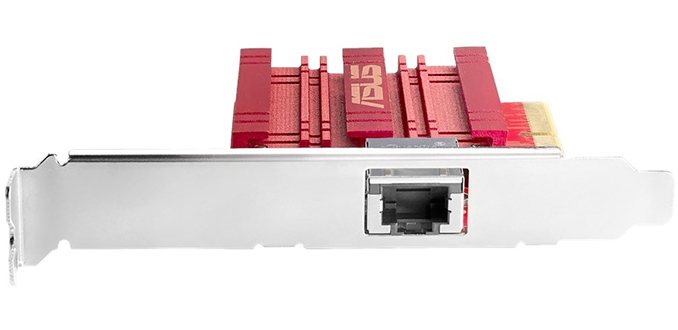
The ASUS XG-C100C is a single port card based on the Aquantia AQtion AQC107 controller that supports five networking standards (100M, 1G, 2.5G, 5G and 10G) and uses a PCIe 3.0 x4 interface. The card is equipped with LEDs that track network activity and connection speed to make it easier for consumers to set up their networks. As for compatibility, the board is compatible with any modern PC running Microsoft Windows 7 and higher, as well as various Linux operating systems.

The XG-C100C board uses a small red PCB as well as a red aluminum cooler to emphasize that it is aimed at higher-end gaming desktops rather than at workstations or servers. It is noteworthy earlier this year ASUS launched its ROG Areion 10G card that is based on the same AQtion AQC107 chip for around $200. That card uses a black PCB with a larger cooling system. Apparently, the design is the only differences between the XG-C100C and the ROG Areion 10G, and the new pricing might indicate the ROG card coming down in price.
The ASUS XG-C100C is available now from various retailers in North America and carries a $99 price tag. It is interesting to note that Aquantia itself sells its AQC107-based cards for about $130. For some reason, ASUS decided to drop the price to a sub-$100 level, possibly, to boost demand. Considering the fact that the Intel X540 and Intel X550-powered cards are sold for $250 to $380, the $99 price point seems very aggressive (albeit still quite high for a network card).ASUS 10GBase-T Cards Based for Consumers XG-C100C ROG Areion 10G Controller Aquantia AQC-107 100BASE-T Yes 1000BASE-T Yes 2.5GBASE-T Yes 5GBASE-T Yes 10GBASE-T Yes (over Cat6 cables) Ports 1 Dimensions (L×W×H) 12 × 8.46 × 2.05 cm 13.5 × 6.3 × 1.9 cm Price $99 ~$200 Release Date June, 2017 April, 2017 Additional Information Link Link
Buy ASUS XG-C100C 10GbE NIC on Amazon.com
As reported previously, the cost of switches and access points is a major concern surrounding the transition to 2.5G/5G/10G for home and SMB. Even though Aquantia is working with its customers to bring lower-cost switches to the market, they are still not available. In the meantime, both Amazon and Newegg are offering the ASUS XG-U2008 10GBase-T network switch for $229 after rebate.
Related Reading:
- ASUS XG-U2008 10GBase-T Network Switch Released: 2x10G + 8x1G for $249
- Lower Cost 10GBase-T Switches Coming: 4, 5 and 8-port Aquantia Solutions at ~$30/Port
- Aquantia Launches New 2.5G/5G Multi-Gigabit Network Controllers for PCs
- Aquantia Launch AQtion 5G/2.5G/1G Multi-Gigabit Ethernet Cards (NICs) for PCIe
- GIGABYTE Exhibits an Aquantia AQC107 based 10G Ethernet PCIe Card
- AKiTiO Displays Thunderbolt 3 to 10GBase-T Adapter
More...
-
07-03-17, 11:02 AM #7132
Anandtech: GIGABYTE Joins AM4 Mini-ITX Club with GA-AB350N-Gaming Wi-Fi Motherboard
GIGABYTE has announced its first Mini-ITX motherboard for AMD’s AM4 processors. The GA-AB350N-Gaming WIFI (or simply AB350N-Gaming) Mini-ITX is based on AMD’s ‘performance-class’ B350 chipset and provides modern features like USB 3.1 Gen 2, support for PCIe 3.0 x4 SSDs, Wi-Fi 802.11ac connectivity and even LED lights and controls. In addition, the motherboard can support large CPU coolers such as AMD’s Wraith Max.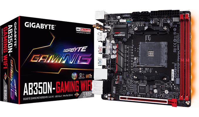
The GIGABYTE GA-AB350N-Gaming WIFI runs AMD’s ‘performance’ B350 chipset that is very similar to the flagship X370, but has some minor differences for market segmentation. B350 still fully supports overclocking of CPUs with an unlocked multiplier, but it should be noted that it cannot take advantage of the XFR feature of the Ryzen X processors.
Given the fact that the AB350N-Gaming WIFI is a Mini-ITX motherboard, the vast majority of its owners are not going to need a PCIe 3.0 x1 slot for add-in-boards, whereas the PCIe 3.0 x16 for a graphics card is handled by the CPU. DRAM space is limited, so one DIMM per channel here.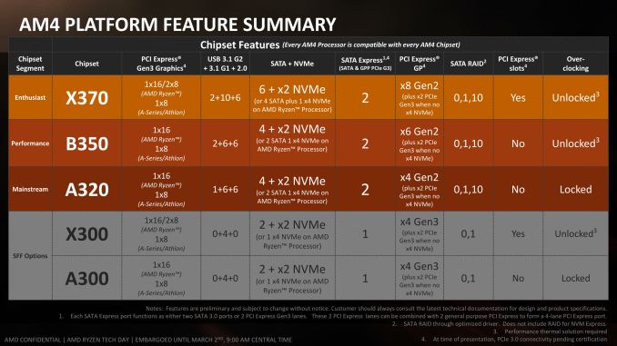
Speaking of overclocking and CPU support in general, the motherboard comes with an advanced all-digital six-phase VRM that uses an International Rectifier controller, IR PowIRstage ICs and solid-state capacitors. The VRM can support all existing AMD Ryzen processors as well as AM4 APUs and has reportedly been designed to have headroom for overclocking. Furthermore, the GA-AB350N-Gaming WIFI comes with 4-pin hybrid fan headers that are specified to liquid cooling systems. As for DRAM, GIGABYTE claims that the motherboard supports up to 32 GB of ECC or non-ECC memory running at up to 3200 MT/s when overclocked.
Like many other Mini-ITX motherboards, the GIGABYTE GA-AB350N-Gaming WIFI is equipped with one PCIe 3.0 x16 slot, one M.2 slot for PCIe 3.0 x4 or SATA SSDs, as well as four SATA ports. When it comes to networking, the mainboard comes with a GbE port enabled by a Realtek controller (with cFosSpeed network traffic management app that aims to reduce network latency) as well as an 802.11ac Wi-Fi + Bluetooth 4.2 module from Intel. As for other I/O, everything seems to be pretty typical here: the motherboard has two display outputs (DP 1.2, HDMI 1.4), two USB 2.0 ports, four USB 3.0 headers, two USB 3.1 connectors (both Type-A) as well as a 7.1-channel audio sub-system powered by the Realtek ALC1220 codec. Finally, for users to make things look 'beautiful', the Mini-ITX AM4 mainboard has six RGB LEDs, as well as two 5-pin onboard headers for other RGB/UV LED strips.GIGABYTE's Mini-ITX Motherboard for AMD Ryzen AB350N-Gaming WIFI CPU Support CPUs in AM4 form-factor
AMD Ryzen and AMD A-series APUsGraphics PCIe 3.0 x16 Chipset AMD B350 Memory Two DDR4 DIMM slots Ethernet Realtek 8111 GbE controller Display Outputs 1 × HDMI 1.4 for APUs
1 × DisplayPort 1.2 for APUsStorage 4 × SATA 6 Gbps
1 × M.2 (PCIe 3.0 x4 or SATA)Audio Realtek ALC1220
7.1 channel audioUSB 4 × USB 3.0 Type-A (+ 2 through internal header)
2 × USB 3.1 Type-A
2 × USB 2.0 (+ 2 through internal header)Other I/O 802.11ac Wi-Fi 1x1 (Intel AC 3160)
Bluetooth 4.2
PS/2 connectorForm-Factor Mini-ITX MSRP $150 ~ $160
GIGABYTE’s GA-AB350N-Gaming WIFI is the fifth Mini-ITX motherboard in the industry that supports AMD Ryzen processors. The product will compete against ASRock’s X370 Gaming ITX/ac (as well as its B350-based brother) as well as Biostar’s Racing X370GTN and Racing B350GTN. Biostar’s motherboards do not have Wi-Fi (but have a DVI-D output), but GIGABYTE’s product is the only one that lacks USB-C (but has two USB 3.1 Type-A connectors). In the end, users are going to have five options (with their own strong and weak sides) to choose from and the only question is their actual availability timeframe because right now none are available.
GIGABYTE did not announce pricing or arrival date for its AB350N-Gaming WIFI motherboard. Common logic tells me that an AMD B350-based motherboard should cost less than an AMD X370-powered platform, but in reality, pricing will depend on supply, demand and willingness of resellers to capitalize on a nearly exclusive product. Ian says that in a perfect world, we'll have a round-up of said boards. Timeframe unknown.
Gallery: GIGABYTE GA-AB350N-Gaming WIFI


Related Reading:
- ASRock Gives AMD Ryzen Mini-ITX Treatment, Launches X370 Gaming ITX/ac
- AMD Announces Ryzen 5 Lineup: Hex-Core from $219, Available April 11th
- AMD Announces Ryzen AGESA 1.0.0.6 Update: Enables Memory Clocks Up To DDR4-4000
- BIOSTAR Reveals Two AMD AM4 Crypto Mining Motherboards
More...
-
07-03-17, 01:05 PM #7133
Anandtech: Nokia 6 to Hit U.S. Market on July 10: 5.5-inch LCD, Snapdragon 430, $229
HMD Global has announced that it would begin sales of its Nokia 6 smartphone in the U.S. in early July. The product will be available in two colors and only from Amazon initially. The company plans to add two more colors to the lineup sold in the U.S. later this summer. It is noteworthy that the "official" Nokia 6 for the U.S. will cost less than it does in China, but will also come with a lower amount of RAM and NAND than on some other versions.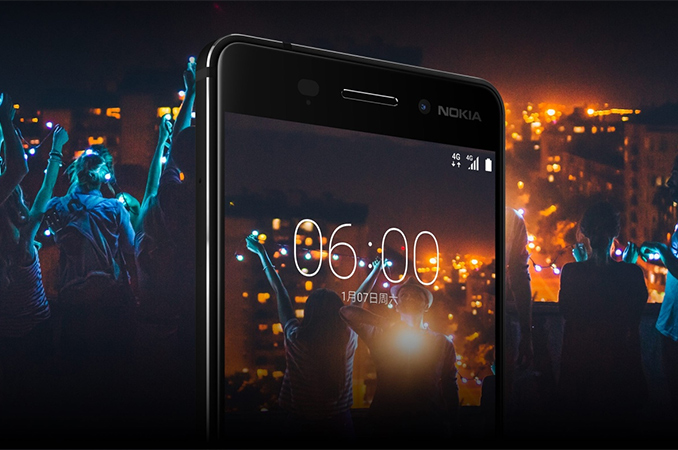
The Nokia 6 is currently the most advanced smartphone offered by HMD Global, which owns rights to produce phones and tablets under the brand. HMD and FIH Mobile (a subsidiary of Foxconn) jointly designed the smartphone with some input from Nokia itself. For the time being, all Nokia smartphones run pure Google Android 7.1 OS with all the upgrades, but no enhancements from the developers.
Visual aesthetics has always been a strong side of Nokia phones in the past and the Nokia 6 is not an exception. The handset comes in a 6000-series aluminum uni-body enclosure with flat edges that are milled using a CNC machine from a single brick of aluminum. To apply color, the chassis is anodized twice and then polished “no less than” five times to make everything smooth. At present, HMD Global offers the Nokia 6 in four colors: matte black, silver, blue and copper. As for the display, the handset is outfitted with a 5.5-inch FHD IPS display featuring 450 nits brightness, enhanced with a polarizer film and covered with round-edge 2.5D Gorilla Glass for protection.
At the heart of Nokia 6 there is the Qualcomm Snapdragon 430 SoC (eight ARM Cortex-A53 cores up to 1.4GHz, an Adreno 505 GPU, an integrated X6 LTE modem) equipped with 3 GB of LPDDR3 RAM and 32 GB of internal NAND flash memory (4GB/64GB for China and Global SKUs). For local connectivity, the phone uses 802.11ac Wi-Fi, Bluetooth 4.1 and a microUSB port. As for imaging capabilities, the smartphone is armed with a 16 MP sensor featuring f/2.0 aperture, autofocus and a dual LED flash on the back as well as an 8MP sensor with f/2.0 aperture on the front. An improvement over many inexpensive phones, the Nokia 6 has stereo speakers coupled with NXP TFA9891 amplifiers and Dolby Atmos software enhancement. The smartphone is powered by a 3000 mAh battery, which is in line with other smartphones in this class.
Buy Nokia 6 International Model on Amazon.comNokia 6 (U.S. Version) Specifications SoC Qualcomm Snapdragon 430 (MSM8937)
8x ARM Cortex-A53 @ 1.4 GHz
Adreno 505RAM 3 GB LPDDR3
4 GB model for China+Global SKUsStorage 32 GB (eMMC) with microSD slot
64 GB model for China+Global SKUsDisplay 5.5-inch 1920x1080 (403 ppi) with 2.5D Gorilla Glass Network 4G: Cat. 4 (Bands: 1, 3, 5, 7, 8, 20, 28, 38, 40)
3G: WCDMA (Bands: 1, 2, 5, 8)
2G: GSM/EDGE (850/900/1800/1900)LTE Down: 150 Mb/s
Up: 75 Mb/sAudio Stereo speakers
3.5-mm TRRS audio jack
NXP TFA9891 amplifiers
Dolby Atmos supportDimensions 154 × 75.8 × 7.85 mm Rear Camera 16 MP with f/2.0 aperture and dual LED flash Front Camera 8 MP with f/2.0 aperture Battery 3000mAh OS Android 7.1 Connectivity 802.11ac Wi-Fi, Bluetooth 4.1, microUSB 2.0 Navigation GPS, GLONASS SIM Size 2x NanoSIM Colors Matte black, silver, blue, copper Price $229.99 for 3GB/32GB Standard Model
$179.99 for Ad Supported Model
$338.99 for 4GB/64GB International Model
The Nokia 6 in matte black and silver will be available for $229.99 from Amazon starting July 10. The smartphones featuring blue and copper finishes will be on sale later this summer on August 18th. Amazon Prime members can pre-order Nokia 6 in various colors with Lockscreen Offers & Ads for $179.99. In addition, Amazon offers the Nokia 6 International model with 4 GB of RAM and 64 GB of NAND for $339 and without any warranty.
Nokia 6 (U.S. Version) Operator Network Compatibility
Data by HMD GlobalCarrier Compatibility Rating Voice/Text 2G 3G 4G LTE AT&T Partially supported + Bands 29 and 30 not supported Sprint No services - T-Mobile Supported + Verizon Wireless No services - Related Reading:
- Nokia 6 Announced: Qualcomm Snapdragon 430, 5.5-Inch Display, Android 7
- HMD Closes Nokia Brand and Patents Deal with Microsoft, Smartphones Due in 2017
- Nokia Is Set to Return to Smartphones and Tablets: What to Expect?
- Microsoft Streamlines Its Smartphone Business Again, Lays Off 1850 People
- HP’s Elite x3 Windows 10 Smartphone to Cost $699, Set to Be Available Worldwide
More...
-
07-03-17, 01:47 PM #7134
Anandtech: Toshiba's 768Gb 3D QLC NAND Flash Memory: Matching TLC at 1000 P/E Cycles?
Toshiba last week announced its first 3D NAND flash memory chips featuring QLC (quadruple level cell) BiCS architecture. The new components feature 64 layers and developers of SSDs and SSD controller have already received samples of the devices, which Toshiba plans to use for various types of storage solutions.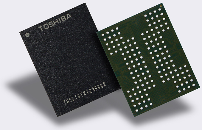
Toshiba’s first 3D QLC NAND chips feature 768 Gb (96 GB) capacity and uses 64 layers, just like the company’s BICS3 chips with 256 Gb and 512 Gb capacities launched in 2016 and 2017. Toshiba does not share further details about its 3D QLC NAND IC (integrated circuit), such as page size, the number of planes as well as interface data transfer rate, but expect the latter to be high enough to build competitive SSDs in late 2018 to early 2019 (that’s our assumption). Speaking of applications that Toshiba expects to use its 3D QLC NAND ICs, the maker of flash memory mentions enterprise and consumer SSDs, tablets and memory cards.
Endurance++
Besides intention to produce 768 Gb 3D QLC NAND flash for the aforementioned devices, the most interesting part of Toshiba’s announcement is endurance specification for the upcoming components. According to the company, its 3D QLC NAND is targeted for ~1000 program/erase cycles, which is close to TLC NAND flash. This is considerably higher than the amount of P/E cycles (100 – 150) expected for QLC by the industry over the years. At first thought, it comes across a typo - didn't they mean 100?. But the email we received was quite clear:
- What’s the number of P/E cycles supported by Toshiba’s QLC NAND?It is unclear how Toshiba managed to increase the endurance of its 3D QLC NAND by an order of magnitude versus initially predicted. What we do know is that signal processing is more challenging with QLC than it is with TLC, as each cell needs to accurately determine sixteen different voltage profiles (up from 2 in SLC, 4 in MLC, and 8 in TLC).
- QLC P/E is targeted for 1K cycles.
The easiest way to handle this would be to increase the cell size: by having more electrons per logic level, it is easier to maintain the data and also read from it / write to it. However, the industry is also in a density race, where bits ber mm^2 is an issue. Also, to deal with read errors from QLC memory, controllers with very advanced ECC capabilities have to be used for QLC-based SSDs. Toshiba has its own QSBC (Quadruple Swing-By Codes) error correction technique, which it claims to be superior to LDPC (low-density parity-check) that is widely used today for TLC-powered drives. However, there are many LDPC implementations and it is unknown which of them Toshiba used for comparison against its QSBC. Moreover, there are more ECC methods that are often discussed at various industrial events (such as FMS), so Toshiba could be using any or none of them. The only thing that the company tells about its ECC now is that it is stronger than 120 bits/1 KB used today for TLC. In any case, if Toshiba’s statement about 1000 P/E cycles for QLC is correct, it means that that the company knows how to solve both endurance and signal processing challenges.
The main advantage of QLC NAND is increased storage density when compared to TLC and MLC, assuming the same die size. As was perhaps expected, die size numbers were not provided. However, last year Toshiba and Facebook talked about a case study QLC-powered SSD with 100 TB of capacity for WORM (write once read many) applications and it looks like large-capacity custom drives and memory cards will be the first to use QLC for cold storage. P/E cycles and re-write endurance isn't a concern for WORM at this stage.
Toshiba has begun to sample its 3D QLC NAND memory devices earlier this month to various parties to enable development of SSDs and SSD controllers. Taking into account development and qualification time, Toshiba plans to mass produce its BiCS3 768 Gb 3D QLC NAND chips around the same time it starts to make its the next generation BiCS4 ICs. The latter is set to hit mass production in 2018, but the exact timeframe is yet to be determined.
Related Reading:
- Western Digital Announce BiCS4 3D NAND: 96 Layers, TLC & QLC, Up to 1 Tb per Chip
- Toshiba Selects Japan-U.S. Consortium As Preferred Buyer For Memory Business
- Toshiba Introduces XG5 Client NVMe SSD
- Western Digital Ships Client SSDs Based on 512 Gb 3D TLC NAND Chips
- Toshiba Samples 64-Layer 512 Gb BiCS 3D NAND, Announces 1 TB BGA SSD
- Toshiba Finalizes Plans for New 3D NAND Fab: Coming Online in 2019
More...
-
07-05-17, 08:56 AM #7135
Anandtech: TerraMaster D2-310 Storage Enclosure (2x 2.5"/3.5" SATA to USB 3.1 Gen 2 T
Storage bridges come in many varieties within the internal and external market segments. On the external side, they usually have one or more downstream SATA ports. The most popular uplink port is some sort of USB connection. Within the USB storage bridge market, device vendors have multiple opportunities to tune their product design for specific use-cases. The TerraMaster D2-310 is a 2-bay direct-attached storage device, supporting both 2.5" and 3.5" drives. It connects to the computer using a USB 3.1 Gen 2 Type-C port. Today's review looks at the unit's performance with SSDs and HDDs. It also covers power consumption and RAID rebuild aspects.
More...
-
07-05-17, 08:56 AM #7136
Anandtech: NVIDIA and Baidu Sign Multi-Facet AI Tech Partnership for Tesla, DRIVE PX2
This morning NVIDIA and Chinese Internet juggernaut Baidu are announcing that they have signed a multi-faceted AI technology partnership that will see the Internet giant utilize NVIDIA’s hardware for several of their products and services. At the same time, ahead of the launch of the SHIELD TV in China, the deal sees NVIDIA turning to Baidu to get Baidu’s technology on NVIDIA’s STB.
Taking place at Baidu Create (Baidu’s AI developer conference), overall the two companies are announcing four different business collaborations for AI. Arguably the biggest of these is that Baidu’s popular cloud computing service – the aptly named Baidu Cloud – will be adding NVIDA’s latest generation Tesla hardware to their service. Baidu Cloud will be adding NVIDIA’s forthcoming Volta-based Tesla V100 for high performance training and inference to their service, along with the Tesla P4s for mainstream inference. This is a continuation of the companies’ existing partnership that takes it into the Volta generation, building on top of Baidu Cloud’s current Tesla P40 offerings.
Along those lines, the second collaboration between the two companies is that Baidu and NVIDIA are committing to optimizing Baidu’s PaddlePaddle (PArallel Distributed Deep Learning) framework for Volta. Baidu makes significant use of PaddlePaddle internally – making this a step in allowing more of their projects on NVIDIA hardware – but the company also publishes the framework under an open source license. So for NVIDIA, this gets Volta support into another major open source framework.
Meanwhile the third collaboration will see NVIDIA and Baidu further cement their ongoing relationship with Project Apollo, Baidu’s open access self-driving car platform, which the company announced earlier this year. The two companies were already working on Apollo, and with today’s announcement Baidu is adopting NVIDIA’s DRIVE PX2 system as the hardware basis for the Apollo platform. Like most DRIVE PX2-related announcements, don’t expect to see DRIVE PX2 showing up in any commercial cars, but rather this sets the stage for developers to begin designing systems now that will ultimately run on Xavier.
Finally, for their own consumer electronics, NVIDIA will be tapping into Baidu’s ecosystem by adopting Baidu’s Duer voice assistant for the SHIELD TV set top box. In most of the world, NVIDIA’s STB is heavily integrated with Google’s services – including the forthcoming addition of Google Assistant support – an obvious hitch for NVIDIA in China as most Google services are blocked there. As a result, the company is instead turning to Baidu to provide the Duer voice assistant for the box. At the same time, while not the focus of today’s partnership announcements, this does confirm that the SHIELD TV will finally be getting a formal release in China, with NVIDIA stating that the STB will be available this year.
More...
-
07-05-17, 12:24 PM #7137
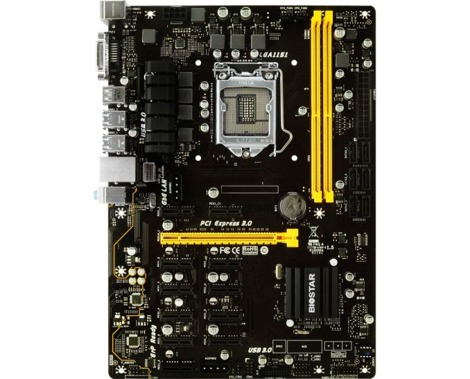
Anandtech: Biostar Goes Mining: New TB250-BTC PRO Motherboard and RX 470D Mining GPU
With cryptocurrency mining specific motherboards and even graphics cards becoming the new normal for certain manufacturers in their offerings, Biostar has thrown two new products into the ring: the TB250-BTC PRO motherboard and VA47D5RV42 (Mining) graphics card. Announced with a formal press release, the TB250-BTC PRO is actually an upgrade to the TB250-BTC that was first seen at Computex 2017. Meanwhile, the US product page for the VA47D5RV42 (Mining) card was quietly posted a couple months ago, interestingly detailing the AMD Radeon RX 470D as its GPU.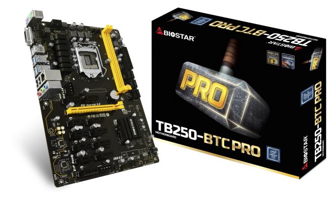
Biostar TB250-BTC PRO
In the context of the recently announced AM4-based cryptomining TA320-BTC and TB350-BTC, the TB250-BTC PRO is a different addition to Biostar’s mining motherboard lineup. As the headliner, Biostar emphasizes the TB250-BTC PRO’s capability to handle 12 GPUs at once with 12 native PCIe slots, just below ASRock’s literally one-upping 13 PCIe slot H110 Pro BTC+. However, it’s important to note that thanks to the B250 chipset the TB250-BTC PRO’s slots are all native PCIe 3.0, while the H110 Pro BTC+ additional 12 PCIe slots are some combination of PCIe 1.0 and PCIe 2.0. Biostar makes sure to explicitly highlight that advantage over the H110 chipset, citing benefits to mining stability and compatibility in having native slots. This is despite the fact that most OSes have trouble with so many cards, but both companies have stated that this is for 'future proofing'.
 The slots themselves are arranged to accommodate PCIe to USB risers and the different arrangement is claimed by Biostar to avoid potential short circuits. The board comes with two Molex and two PCIe 12V 4pin power connectors on the motherboard to deal with the power draw. And if Biostar wasn't obvious in firing a shot across the ASRock bow earlier, they certainly are here: the below image from Biostar's website shows an even arrangement of occupied PCIe slots, and is compared to the H110 Pro BTC+'s arrangement.
Biostar TB250-BTC Cryptomining Motherboards TB250-BTC PRO TB250-BTC CPU Support Intel Core i7/i5/i3/Pentium/Celeron
LGA 1151
95W TDP maxChipset Intel B250 Expansion Slots 1 x PCIe x16 3.0
11 x PCIe x1 3.01 x PCIe x16 3.0
5 x PCIe x1 3.0Memory 2 x DDR4 DIMM slots Ethernet Realtek RTL8111H Display Outputs 1 x DVI-D Storage 6 × SATA3 6 × SATA3
1 × M.2 (PCIe 3.0 x4 or SATA)Audio Realtek ALC887
8 channel HD audioI/O 1 x PS/2 Mouse
1 x PS/2 Keyboard
4 x USB 3.0 Port
2 x USB 2.0 Port
2 x USB 2.0 Port (5V, up to 1.5A)
1 x DVI-D Connector
1 x RJ-45 Port
3 x Audio ConnectorForm-Factor ATX Price TBA $95
Compared to the standard TB250-BTC, Biostar advertises the sheer advantage in additional graphics cards capability (6 vs. 12) as saving a total of $200 in initial cost compared to using two TB250-BTC systems. The motherboard also has what Biostar calls ‘Hybrid Mining’ technology that "supports multiple AMD and NVIDIA cards simultaneously," but details thereof are very light aside from just putting them in and letting the drivers manage. In this case, the vagueness is unhelpful since most mining software is already capable of handling mixed AMD/NVIDIA setups.
Gallery: TB250-BTC PRO


Biostar VA47D5RV42As for the cryptomining card, Biostar has intriguingly based the VA47D5RV42 (Mining) off the AMD Radeon RX 470D GPU. As a product for the Chinese market only, the original RX 470D was quietly launched last year without any official announcement outside of China. To describe briefly, the RX 470D is a further cut-down configuration of Polaris 10, having 1792 stream processors as opposed to RX 470’s 2048. In terms of non-Chinese documentation, this is the first time the RX 470D has officially shown up.
It is unclear how much of a mining-specific SKU Biostar’s card is, as the product page states it supports the all usual display outputs (1x DVI, 3x DP, 1x HDMI). The custom cooler equipped VA47D5RV42 (Mining) card appears to be custom clocked as well, with its 4 GB of VRAM clocked at 7000 MHz. Unlike ASUS and Sapphire’s cryptocurrency cards, the VA47D5RV42 (Mining) has not surfaced in any online retailer catalogues in any form, making it hard to state that Biostar has released the card in the traditional sense. If anything, listing the RX 470D mining card on the US product pages suggests that the RX 470D may eventually semi-officially show up outside China, an odd conclusion given that AMD had ostensibly produced the RX 470D for the specific channel needs and consumer demands of the Chinese market.
For the TB250-BTC PRO, Biostar has not revealed pricing or availability dates.
More...
-
07-06-17, 09:51 AM #7138
Anandtech: Mining Cards Update: Zotac, Manli and Biostar Products Formally Confirmed
Although ASUS and Sapphire cryptocurrency mining cards were officially outed last week, other pieces of evidence have suggested other vendors were also producing cryptomining cards. Both the GPU manufacturers (AMD and NVIDIA) and their board partners have remained tight-lipped, with only ASUS announcing via press release about their cryptomining hardware endeavors. Since then, product pages for cards have emerged for Manli, Zotac, and Biostar.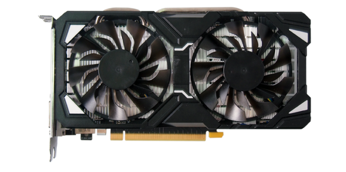
Manli, a PC Partner sub-brand focused on the Asia/China region, has listed product pages and datasheets for two cryptocurrency mining cards and one mining system containing many cards: the P106-100 Mining Card (F336G), the P106-100 Mining Card (F347G), and GPU Mining System (M-P1061008-N). Meanwhile, Zotac, another sub-brand of PC Partner more familiar in the West, has listed a product page on its Chinese website for P106-100; the English/Global site does not have the page. And as covered earlier, Biostar outed their VA47D5RV42 (Mining) card, a custom version of the China-exclusive AMD Radeon RX 470D.
The MANLI P106-100 Series
Both Manli P106-100 cards are roughly equivalent to the NVIDIA GTX 1060 6GB, equipped with the same GP106 GPU at GTX 1060 reference clocks alongside 6GB of GDDR5 VRAM. Both are outfitted with custom two-fan open air coolers, and lack display outputs. At a glance, the F336G variant appears to have the same cooler as the Manli GTX 1060 6 GB (F336G), albeit without stickers or labels, while the F347G resembles the Manli GTX 1060 Gallardo. Interestingly, the package size for both cards is noted as ‘bulk pack,’ as opposed to the typical box dimension measurements for Manli’s other graphics cards. This indicates that the products are purchased in bulk and are not packaged or intended for individual sale.
Moving on, Manli’s GPU Mining System (M-P1061008-N) is a pre-assembled mining rig with 8 preinstalled passively-cooled ‘Nvidia P106-100 mining cards’ and an optional 1600W PSU. A mobile Intel Celeron CPU runs the system, accompanied with 1 stick of 4GB DDR3 and a 64GB mSATA SSD with an optional Windows 10 installation. The custom motherboard has 9 PCIe x16 slots and 7 12V 6pin connectors, all cooled by 10 9cm 4500RPM fans. As for outputs, the rig has an HDMI port, a ‘Giga LAN’ RJ45 port, and 2 USB 2.0 ports. Essentially, the system looks like a server, and certainly will make a noise like one.
Zotac's P106-100
Like Manli’s GP106-based cards, Zotac’s P106-100 is reference clocked and does not support any display outputs. It seems like Zotac rehashed (no pun intended) the preexisting Zotac GTX 1060 6GB Galaxy HB two-fan custom cooler for the P106-100 mining card. In fact, as careful readers will notice, the Zotac P106-100 custom cooler closely resembles the Manli F336G card coolers. As Zotac and Manli are sub-brands of PC Partner, this commonality is entirely reasonable, and perhaps expected.

Announcements So Far
Summing up the companies, Manli, Zotac, and Biostar join ASUS and Sapphire in officially releasing mining-specific video cards. Relatedly, China-only P106-100 mining cards from MSI and Galax were shown in an unboxing video last week. In total, most of the world’s largest graphics card vendors are releasing cryptomining cards, with PC Partner represented through Zotac and Manli, and Palit being represented by sub-brand Galax. Given that Manli and Zotac appear to have utilized the same GTX 1060 custom cooler, it is not unreasonable to expect a mining card from PC Partner's third sub-brand, Inno3D. Yet with all the hardware out and about, only ASUS has packaged and announced products for individual sale: the MINING series. Otherwise, it is clear that there is a heavy focus on the Chinese market and on large-scale bulk purchasers.
These trends bring up a number of points. Board partners are not aggressively attacking the traditional consumer market with these cards, preferring to keep quiet publicly. If it turns out that mining demand is centered on China, segmenting the market this way isolates the lucrative US and Europe spheres from mining card contamination and bad publicity. Likewise, if mining demand is indeed centered on distributors, organized groups, and bulk purchasers rather than hobbyist cryptominers, standard consumers are shielded in the same way while the problem is solved out of the public eye.
In context, manufacturers are still dealing with the same issues brought up in our first cryptocurrency mining cards article: overproduction leading to oversupply, RMA/warranty concerns, sales cannibalization by way of old inventory and a flooded secondary market, and brand damage (e.g. used cards in poor health, association with mining farms).
The overproduction issue has been misinterpreted by some to mean that production is maxed and so manufacturers are incapable meeting inflated demand, which is incorrect because they are capable. Much of the problem is the turnaround time, as the time between the decisions to increase production and the extra products hitting the shelves are in the order of several months or longer. In addition, increased production would last for a minimum of several months. Depending on how severely supply is starved, board partners might be waiting on AMD and NVIDIA, who themselves might be waiting on GlobalFoundries and TSMC, before they can even stick the GPU on a custom PCB and cooler, not to mention putting it in a box and shipping it out. For something as volatile as cryptocurrency mining, a currency crash during those in-between months would be catastrophic. Ordering higher production is relatively easy; getting rid of excess unsellable inventory because demand crashed too soon is hard.
For mining-specific cards, the stakes are doubled, as excess niche mining cards would be even more difficult to sell. In that regard, ROI-focused cryptominers take into account the inherent resale value of consumer graphics cards. If mining SKUs are too enticing for cryptominers, so much that consumers start to partake, manufacturers have to deal with market segmentation headaches and lower average selling prices. But if mining SKUs are not enticing enough for cryptominers, hobbyists or otherwise, miners will instead keep purchasing consumer cards, leaving board partners with unsold inventory of niche products on top of having no supply to satiate annoyed non-mining consumers. The consequences for that hypothetical failure are less dire outside US/Europe, while mining card success in China would presumably give vendors valuable experience in how to properly market and produce mining cards in the US/Europe. Similarly, producing bulk amounts of brown box cards for distributor back-channels ensures that inventory keeps selling without the risk of adversely affecting the consumer market. And if that resolves the mining demand problem right there and then, then all the better for them – and us.
More...
-
07-06-17, 11:05 AM #7139
Anandtech: Samsungs Multi-Billion Fab in Pyeongtaek Starts Production of 64-Layer V-
Samsung on Tuesday announced that it had started mass production of 64-layer V-NAND memory in its newly build fab in Pyeongtaek, South Korea, and the first batch had already been shipped to one of the company’s customers. The new fab was intended to focus on DRAM manufacturing, but in the light of NAND flash shortage the company adjusted its plans at some point and now the plant produces V-NAND.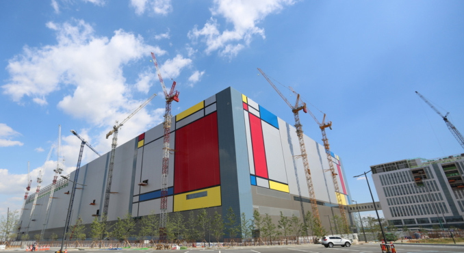
Samsung’s semiconductor manufacturing facility in Pyeongtaek will be the largest and one of the most expensive fabs in the world once it ramps up its production to full capacity. Samsung announced plans to build it in October, 2014, and then started construction in April, 2015. Initially, Samsung announced plans to invest ?15.6 trillion (around $13.5 billion at the current exchange rate) in the facility, but over the past couple of years, it announced further expansion plans for the fab. As a result, investments in the Pyeongtaek facility will total ?30 trillion ($26.1 billion) by 2021, making the complex the most important semiconductor manufacturing facility ever.
According to some reports, Samsung initially planned to produce DRAM in its new fab, but given its size and scale, it was doubtful that the plant would be used only for DRAM. As it appears, Samsung decided to produce fourth-generation 3D V-NAND flash memory in its Pyeongtaek facility first, possibly because there is growing demand for NAND by Samsung’s own divisions, including Samsung Mobile. It remains to be seen when the fab in Pyeongtaek starts to manufacture DRAM ICs, which are also in short supply nowadays. Keep in mind that 3D NAND and DRAM components are produced using completely different process technologies and the former requires some additional equipment. Therefore, Samsung and other memory makers cannot switch from NAND to DRAM and vice versa without some level of equipment adjustment and reconfiguration of fab space.
At present, Samsung does not talk about the number of wafer starts at the Pyeongtaek fab because it is not operating at full capacity. That said, the plant is not going to have a substantial impact on global NAND supply in the coming weeks or months. Once fully ramped several quarters down the road, the Pyeongtaek facility will have a significant impact on both NAND and DRAM industries, as it will increase the output of both types of memory (assuming that it will be used for DRAM in the coming quarters).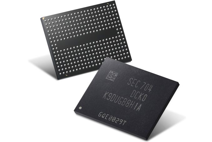
Samsung does not disclose what kind of flash memory chips it produces in terms of capacity and performance, but says that they rely on its 64-layer V-NAND design. So far, the company officially has announced only two 64-layer V-NAND ICs. First is the 512 Gb 3D TLC NAND chip with an 800 MT/s interface data rate that the company demonstrated at the Flash Memory Summit 2016. Second, the 256 Gb 3D TLC NAND IC with a 1000 MT/s interface data rate, the company launched earlier this year and began to produce in high volume in June (presumably at another facility).
Manufacturing of 64-layer 256 Gb chips in at least two facilities indicates that Samsung is ramping up volume production of its fourth-generation V-NAND chips and therefore it is logical to expect new products based on such ICs (e.g., SSDs, memory cards, etc.) to hit the market in the coming months. Among the more interesting products will be higher-end SSDs based on 256 Gb V-NAND chips featuring a faster interface, but it remains to be seen what kind of real-world performance advantages they are going to bring given the bandwidth limitations of PCIe 3.0 x4 bus (used for NVMe M.2 drives), or for smaller capacities. So far, Samsung has only introduced the OEM-oriented PM871b SATA SSDs in 2.5" and M.2 form-factors based on its fourth-gen V-NAND memory.
Related Reading- Samsung at Flash Memory Summit: 64-layer V-NAND, Bigger SSDs, Z-SSD
- Samsung Announces 960 PRO And 960 EVO M.2 PCIe SSDs (Updated)
- The Samsung 960 Pro (2TB) SSD Review
- The Samsung 960 EVO (1TB) Review
- SK Hynix Launches 72-Layer 256 Gb 3D TLC NAND with Increased Performance
- Western Digital Announce BiCS4 3D NAND: 96 Layers, TLC & QLC, Up to 1 Tb per Chip
- Toshiba's 768Gb 3D QLC NAND Flash Memory: Matching TLC at 1000 P/E Cycles?
More...
-
07-06-17, 01:32 PM #7140
Anandtech: EKWB Launches Aftermarket EK-M.2 Aluminum Heatsink for M.2 SSDs
EKWB (EK Water Blocks) on Wednesday introduced a useful but slightly different to their normal routine type of product. The company has started to sell its EK-M.2 NVMe passive heatsinks, designed for consumer M.2 SSDs that matches the design of the company’s water blocks and other components. The device costs €10 – €13, depending on the finish.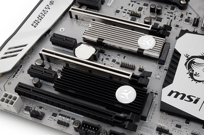
Advantages of M.2 SSDs over consumer drive form-factor drives have been discussed multiple times before: they are smaller, sometimes they are cheaper to make, and they are faster because they use PCIe interface along with NVMe protocol (in most cases). However, they have one main drawback that sometimes affects their performance: they are hard to cool down. Contemporary SSD controllers contain multiple computing cores and perform rather intensive mathematical operations in order to work with modern NAND flash memory properly and correct read errors that occur with the latest types of flash (and thus guarantee their endurance rating). As a result, sometimes those controllers overheat on M.2 drives because of insufficient cooling and begin to throttle, reducing performance. Going forward, SSD controllers will become even more complex, especially as the industry moves to higher bit densities with TLC and then QLC architectures. Developers of such controllers will likely try to keep their TDPs in check by using lower-power compute cores and/or low-power process technologies, but it remains to be seen whether temperatures of next-gen controllers will be lower than temperatures of modern ones.
Various industry players attempt to ensure proper cooling of M.2 SSDs by equipping their drives with thermal pads (Samsung) or heatsinks (Plextor), offering heatsinks with motherboards (MSI) or selling aftermarket thermal pads (Silverstone). Now, EK Water Blocks is throwing its 2c and offering aftermarket M.2 heatsinks for owners of its LCS and other customers.
The EK-M.2 NVMe passive heatsinks are made of aluminum, feature front and back plates, and are equipped with clips to attach them to SSDs. The coolers are compatible with single-sided M.2-2280 drives plugged into M.2 slots that are of 4.2 mm height. Essentially, EK-M.2 NVMe can handle standard consumer SSDs installed into typical desktop motherboards, but compatibility beyond that cannot be guaranteed. According to EKWB, the EK-M.2 heatsink can reduce controller temperature by 8-10°C, or even more with appropriate airflow.

As for pricing, EKWB sells its the EK-M.2 NVMe heatsink with black finish for €9.96, whereas the M.2 SSD cooler with nickel finish costs €12.94 (incl. VAT). The products are available from EKWB’s online store as well as from its resellers.
Gallery: EKWB EK-M.2 NVMe Heatsink


Related Reading:
- EK Water Blocks Announces Aluminum-based Fluid Gaming Series Open Loop Liquid Coolers
- SilverStone Launches SST-TP01-M.2 Thermal Pads for M.2 SSDs
- Intel Announces SSD DC P4501 Low-Power NVMe SSD With 3D NAND
- Plextor Announces M9Pe SSD: 3.1 GB/s, Marvell Controller, 64-Layer 3D TLC, RGB LEDs
- Patriot Preps Budget-Priced & Phison-Based Scorch NVMe SSD For Q3
- Toshiba Introduces XG5 Client NVMe SSD
More...


 Quote
QuoteThread Information
Users Browsing this Thread
There are currently 26 users browsing this thread. (0 members and 26 guests)


Bookmarks