

Results 8,181 to 8,190 of 12091
Thread: Anandtech News
-
05-26-18, 04:28 PM #8181
Anandtech: Two New 35W Raven Ridge Parts: AMD Athlon 200GE and Athlon Pro 200GE
In this interesting world where processors are released but not formally announced, it means that when diving through the lists of supported CPUs on certain motherboards, we might find processors we have never heard of before. Thanks to some sleuthing on Twitter by one of our followers, we can detail that AMD has two new 35W Ryzen processors that we previously did not know about.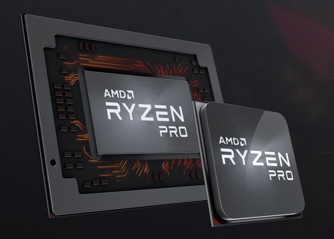
Over on the ASUS Crosshair VII Hero CPU supported list, the two new processors are listed, supported as of BIOS 0509:
Traditionally AMD uses the Athlon name for its combined CPU/GPU processors that have the GPU disabled (which AMD calls its NPUs, or non-accelerated processing units). What makes this interesting is that based on Geekbench data already submitted to the results database (on an ASUS B350M motherboard), these parts both have integrated graphics.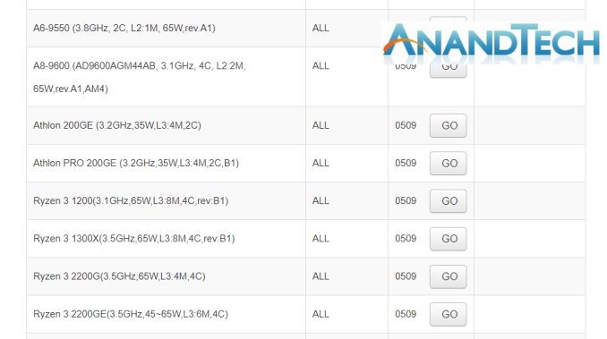
Between the two sources, it shows that the processors are essentially identical, with the difference in the Pro variant being that it falls under AMD’s commercial brand for customer support. The part then is a dual core processor with hyperthreading, running at a base frequency of 3.2 GHz, at a 35W TDP, and either 2 MB or 4 MB of L3 cache (both sources state something different: ASUS lists 4 MB, which is usually more accurate). Neither source states a turbo frequency, so it might come to pass that the Athlon processors do not have any turbo, but also missing is the information about the integrated graphics. Neither ASUS’ support list nor Geekbench traditionally lists this data. Geekbench does list it as a Raven Ridge part (which makes sense, being a CPU+GPU design), which would also mean it is built on 14nm.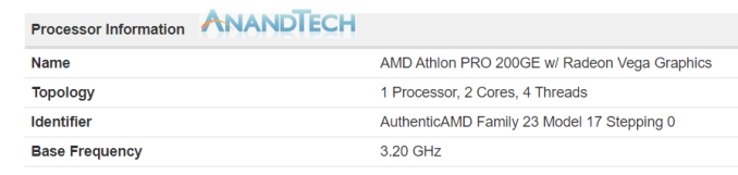
Normally when processors are not announced with the rest of the set, it means one of two things. First, they are not important for the story, and so from a PR perspective it makes sense to the company to leave them out of materials (no matter how much that bothers the media), or that these processors are ‘off-roadmap’, and are built to order from a specific customer. At this point we are unsure of where AMD stands on these parts.Ryzen APUs AnandTech Cores Base Turbo GPU TDP Mobile Ryzen 7 2700U 4C / 8T 2.5 GHz 3.4 GHz Vega 10 15 W Ryzen 7 2700U Pro 4C / 8T 2.2 GHz 3.8 GHz Vega 10 15 W Ryzen 5 2500U 4C / 8T 2.0 GHz 3.6 GHz Vega 8 15 W Ryzen 5 2500U Pro 4C / 8T 2.0 GHz 3.6 GHz Vega 8 15 W Ryzen 3 2300U 4C / 4T 2.5 GHz 3.4 GHz Vega 3 15 W Ryzen 3 2300U Pro 4C / 4T 2.5 GHz 3.4 GHz Vega 6 15 W Desktop Ryzen 5 2400G 4C / 8T 3.6 GHz 3.9 GHz Vega 11 65 W Ryzen 5 2400G Pro 4C / 8T 3.6 GHz 3.9 GHz Vega 11 65 W Ryzen 5 2400GE 4C / 8T 3.2 GHz 3.8 GHz Vega 11 35 W Ryzen 5 2400GE Pro 4C / 8T 3.2 GHz 3.8 GHz Vega 11 35 W Ryzen 3 2200G 4C / 4T 3.5 GHz 3.7 GHz Vega 8 65 W Ryzen 3 2200G Pro 4C / 4T 3.5 GHz 3.7 GHz Vega 8 65 W Ryzen 3 2200GE 4C / 4T 3.2 GHz 3.6 GHz Vega 8 35 W Ryzen 3 2200GE Pro 4C / 4T 3.2 GHz 3.6 GHz Vega 8 35 W Athlon 200GE
YD200GC6M2OFB2C / 4T 3.2 GHz ? ? 35 W Athlon Pro 200GE
YD200GC6M20FBPro 2C / 4T 3.2 GHz ? ? 35 W
It is worth noting that these parts do not have the ‘Ryzen’ name in them.
Given the fact that it is a long weekend in the US, while we have reached out to our contacts at AMD, we are not expecting a response until Tuesday. More information as we get it.
Buy AMD Ryzen 5 2400G on Amazon.com
Update: Computerbase.de reports that these two new processors are set to be announced at Computex, and that both of these parts have Vega 3 graphics.
Related Reading- AMD Launches Ryzen Pro with Vega: Mobile APUs and Desktop APUs
- AMD Launches Ryzen PRO CPUs: Enhanced Security, Longer Warranty, Better Quality
More...
-
05-28-18, 07:43 AM #8182
Anandtech: New Patriot Viper RGB Memory: Up to DDR4-4133
Customizable RGB LED lighting has become ‘a new black’ for enthusiast-class PCs: virtually all manufacturers of nearly all components for advanced computers have already introduced various devices with customizable RGB lights. Patriot is a little bit late to the RGB party with its Viper RGB memory modules (though it has had Viper LED modules for a while), yet these DIMMs arguably look more aggressive than some competing products.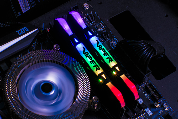
Patriot’s Viper RGB DDR4 modules are outfitted with the company’s brand-new aluminum heat spreaders with the Viper logotype that feature five RGB LED zones each of which can be customized. The RGB LEDs are compatible with software from all major makers of motherboards, including the ASUS Aura Sync, the ASRock Polychrome Sync, the GIGABYTE RGB Fusion, and the MSI Mystic Light Sync. In addition, Patriot will offer its own app to control LEDs on its Viper RGB DIMMs.
Patriot is taking a relatively cautious approach to RGB-enabled memory modules, so the initial lineup of Viper RGB DDR4 kits will include moderate to high-speed speed bins that will top at DDR4-4133 at 1.40 V, which is below 'extreme' offerings from some other makers. Meanwhile, the Viper RGB will be the highest-end modules in Patriot's lineup both in terms of performance and style.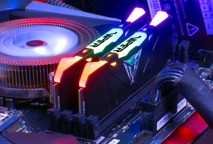
Good news is that all the initial Viper RGB DDR4 kits are compatible with both AMD Ryzen- and Intel Core-based platforms (obviously, keeping in mind frequency-related limitations on Ryzen), so enthusiasts with different kinds of CPUs will not have to worry about compatibility. Meanwhile, the modules feature XMP 2.0 SPD profiles for Intel Core processors, but no special profiles for AMD Ryzen chips, which means that owners of appropriate PCs will have to load all the sub-timings manually.
The Viper RGB DIMMs are based on specially-designed PCBs to support RGB LEDs and to handle higher data transfer rates required from enthusiast-class memory modules. Patriot does not disclose which memory chips it uses for the modules, but we will update you once we obtain such information. In any case, most of contemporary DRAMs can run fine at 3200 - 3600 MT/s with 1.35 V, so the main question is how overclockable the mainstream Viper RGB DIMMs will be.
Gallery: Patriot Viper RGB DDR4Patriot's Viper RGB 2x8 GB Memory Kits Speed CL Timing Voltage Heat Spreader Color PN DDR4-2666 15-17-17-35 1.2 V Black
WhitePVR416G266C5K
PVR416G266C5KWDDR4-3000 1.35 V Black
WhitePVR416G300C5K
PVR416G300C5KWDDR4-3200 16-18-18-36 Black
WhitePVR416G320C6K
PVR416G320C6KWDDR4-3600 16-18-18-36 Black PVR416G360C6K DDR4-4133 19 21-21-41 1.4 V Black PVR416G413C9K 


Patriot’s Viper RGB memory modules will be available starting late May or early June. Pricing will depend on market conditions and all the kits will be covered by a lifetime warranty.
Buy Patriot Viper RGB DDR4-4133 16 GB on Amazon.com
Related Reading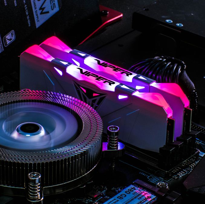
- Mini-Jellyfish: ADATA Launches XPG Spectrix D80 DDR4 RGB Memory
- RGB Fan for Corsair Dominator Platinum DDR4 Launched: $70 MSRP
- Corsair Vengeance RGB DDR4 Memory Modules with LEDs Now on Sale
- Corsair Weds RGB Lighting and White Heat Spreaders in Vengeance RGB White DDR4 DIMMs
- G.Skill Unveils 16GB DDR4-4700 Trident Z RGB DRAM Kit: Samung B-die & RGB LED
- G.Skill Shrinks Latencies of DDR4-4000+ Kits for Coffee Lake: DDR4-4266 CL17 Announced
- GSkill Announces New AMD Compatible Trident Z RGB Kits
- Patriot Publishes List of AMD Ryzen Compatible DIMMs: Up to DDR4-3400, 64 GB
- Patriot Adds Two Dual-Channel DDR4-3733 Memory Kits into Lineup
More...
-
05-29-18, 10:11 AM #8183
Anandtech: Toshiba Memory to Build New Fab to Produce BiCS 3D NAND
Toshiba Memory Corp., which is set to become independent from Toshiba in a few days, has announced their intention to start construction of a new BiCS 3D NAND fab in July. TMC expects Western Digital to participate in the new project. Overall, this is the latest in a number of NAND fab announcements across the industry in the last year that, at long last, signals surging interest in building additional capacity.
The new fab will be located near Kitakami City, Iwate prefecture. By contrast, the existing NAND flash production facilities operated by TMC and Western Digital are located near Yokkaichi, Mie prefecture. Traditionally for Japan, the new fab will feature a quake absorbing structure and an environmentally friendly design, which includes materials used and energy efficient production equipment. Just like the Fab 6, the new production facility will use an AI-powered production system to boost productivity.
Toshiba expects to complete the building sometimes in 2019 (most probably in summer 2019 as it takes around a year to construct a fab building) and then start with equipment move-in. This process usually takes two to three quarters, so expect the new fab to come online in 2020, if everything goes as planned.
Until the company makes its final decision regarding the manufacturing tools to be used, the actual production capacity of the new fab is unknown. Meanwhile, decisions regarding equipment will be made based on multiple factors, including predicted demand for NAND and Western Digital’s participation in the project. Speaking of Western Digital. Late last year Western Digital announced that it would participate in building the fab in Iwate, but so far, the company has not made any announcements regarding its exact plans on the matter.
Toshiba last week announced that it had received all the required anti-trust regulatory approvals regarding its sale of Toshiba Memory Corp. (TMC) to Pangea consortium of investors. The last regulator to approve the $18-billion transaction was China. The deal is now expected to close on June 1, as planned by the Japanese company.
Buy Toshiba OCZ RD400 512 GB SSD on Amazon.com
Related Reading:
- Toshiba Finalizes Plans for New 3D NAND Fab: Coming Online in 2019
- Toshiba to Build New Fab to Produce BiCS NAND Flash
- Toshiba Signs Deal To Sell Memory Business
- Western Digital, Toshiba And Bain Capital Settle Disputes Over Sale Of Toshiba Memory
- Toshiba To Proceed With Sale Of Memory Business To Consortium
More...
-
05-29-18, 10:11 AM #8184
Anandtech: Western Digital: 96-Layer 3D NAND Progressing Well, Shipping to Retail Cus
Western Digital this month said that it had started shipments of its fourth-generation BiCS 3D NAND memory to some of its customers. The company did not disclose details, but only said that the 96-layer 3D NAND memory is used for storage devices sold in retail, which usually means that it is used for inexpensive flash drives and/or memory cards. One of the important things about Western Digital’s BiCS4 memory is the manufacturer’s plan to build both TLC and QLC NAND using the technology.
Western Digital started production of its 96-layer BiCS4 NAND memory earlier this year and confirmed the beginning of the ramp up in late April during a conference call. At the J.P. Morgan Global Technology, Media and Communications conference in mid-May the company said that it had started to ship the said chips for revenue to its retail customers. Western Digital does not give any guidelines regarding the pace of the ramp up and the time when shipments of BICS4 exceed shipments of BICS3, but the fact that the ICs are used commercially is important.
“BiCS4, which is 96 layers, we have introduced that technology and we are shipping it primarily to our retail customers,” said Steve Milligan, CEO of Western Digital. “If you look to where we at from a yield curve perspective, because [BICS4] is not too mature, we are very pleased with where we are. Because once you get to a certain point, you can project where you are going to end at (based on cycles of learning, etc). So, the 96-layer technology is progressing quite well, we continue to increase output of that as we move to the rest of 2018, I am very thrilled and grateful for our strong 3D NAND execution.”
Western Digital’s (and Toshiba’s) BICS4 is a name for a family of 3D NAND flash devices featuring 96 active word lines (or layers). The lineup will include both TLC and QLC chips with capacities ranging from 256 Gb to 1 Tb. Based on Western Digital’s announcement from 2017, its first chips to use 96 word layers are 256 Gb 3D TLC NAND devices. After the manufacturer figures out how to produce 96-layer 3D NAND with sufficient yields, it will move on to higher-capacity 3D TLC and eventually 3D QLC chips with up to 1 Tb (128 GB) capacity.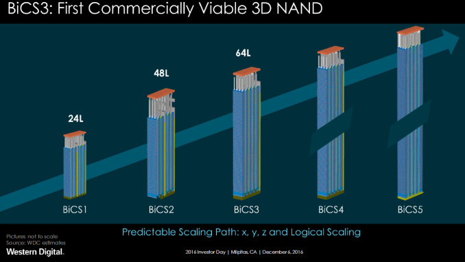
Speaking of QLC, it is necessary to point out that last year Western Digital and Toshiba also announced 768 Gb BICS3 64-layer 3D QLC NAND memory and it is highly likely that such ICs will hit the market earlier than 96-layer QLC NAND. Nonetheless, QLC is a crucial part of Western Digital’s future plans.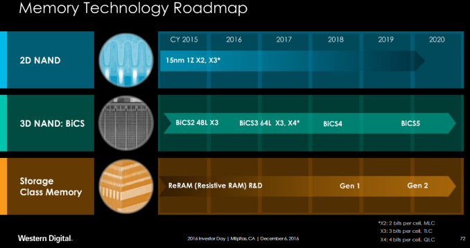
Related Reading: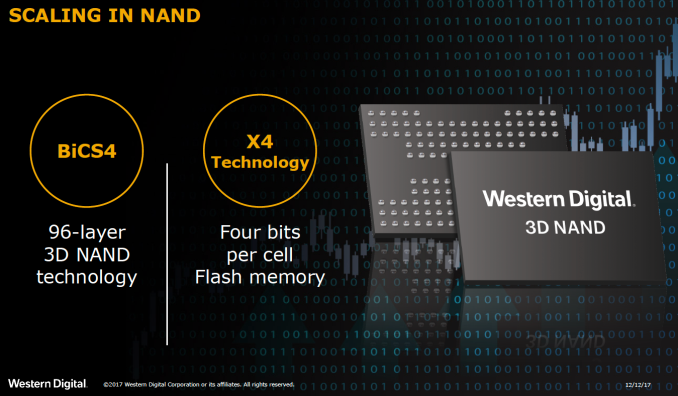
- Western Digital Announce BiCS4 3D NAND: 96 Layers, TLC & QLC, Up to 1 Tb per Chip
- Western Digital Announces Four Bit Per Cell 64-Layer 3D NAND Flash
- Toshiba's 768Gb 3D QLC NAND Flash Memory: Matching TLC at 1000 P/E Cycles?
- Intel And Micron Launch First QLC NAND: Micron 5210 ION Enterprise SATA SSD
Source: Western Digital
More...
-
-
05-29-18, 10:13 PM #8186
Anandtech: Qualcomm Announces XR1 Platform: Dedicated SoC for VR/XR Headsets, Coming
For the better part of the past few years now, Qualcomm has been making a serious and concentrated effort to establish themselves as the dominant player in the mobile VR space. And as the first generation of standalone VR headsets have come out, those efforts on both the hardware side and even more on the software/dev support side are finally paying off. Rivaled only by Samsung’s phone-based Gear VR system, if you’re using a standalone VR headset today, it’s almost certainly powered by a Qualcomm Snapdragon SoC.
Now amidst the backdrop of the annual Augmented World Expo, Qualcomm is taking the next step on the hardware side of matters. This evening the mobile juggernaut is announcing their first dedicated VR/AR/XR platform/SoC, the Snapdragon XR1.
The XR1 is Qualcomm’s first purpose-built silicon for what the company is dubbing eXtended Reality devices, a catch-all term for virtual/augmented/mixed reality. The creation of the platform means that Qualcomm feels the market for standalone headsets has finally grown enough that it’s reached a point where they can justify the costs of a dedicated platform, including the silicon engineering and even more expensive developer and consumer relation campaigns that go with it. In that sense everything up until now has been the company laying the groundwork for this moment – and not that Qualcomm hasn’t been serious up until now – but this marks a significantly higher investment on their part than their efforts up until now.
The XR1 is, in turn, part of what is becoming a two-pronged strategy for Qualcomm on the XR SoC front. Qualcomm sees the mobile headset market as encompassing three markets: entry-level “cardboard” devices used with phones, “high quality” but economically priced 3DoF headsets like the Oculus Go, and then “premium quality” 6DoF headsets like the Lenovo Mirage. Of these three groups, Qualcomm intends to go after the latter two.
For the best experiences, Qualcomm will continue pushing their flagship-class (and flagship-priced) smartphone SoCs like the Snapdragon 845. However for devices like the Oculus Go and other headsets, where cost is a greater concern and vendors are okay with trading-off features to meet mass-market prices, this is the territory Qualcomm is going after with the XR1. In practice then, the XR1 is a successor-of-sorts to the Snapdragon 821 and other older SoCs that have been tapped for these first-generation headsets. It replaces relatively cheap-but-aging SoCs with even cheaper silicon purpose-built for XR headsets and headsets alone; smartphones need not apply.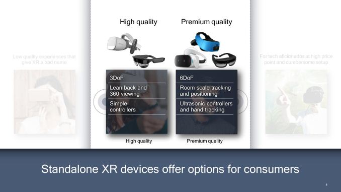
As far as the XR1 SoC itself goes, today’s announcement is a bit of a mixed bag. Unfortunately Qualcomm is not disclosing the specifications of the SoC at this time – so information on the CPU cores used, GPU configuration, etc – are not going to be revealed until closer to the launch. But they are, at a high level, laying out their design and product goals with the XR1, and in the process making some confirmations about what the forthcoming SoC can and cannot do.
At a high level, the XR1 can be thought of as a stripped-down version of a traditional Snapdragon SoC, eschewing the smartphone-specific hardware such as the modem. While Qualcomm isn’t outlining the specifications of the chip, if you’re familiar with the building blocks they use for other Snapdragons then you know where this is going: a Kryo CPU block, an Adreno GPU block, a Spectra ISP block, a Hexagon DSP block, etc.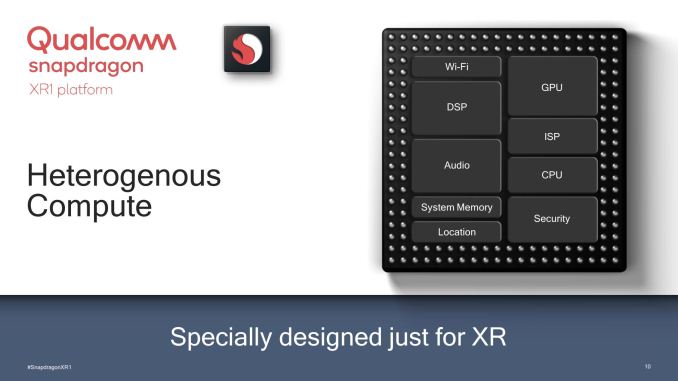
At this point I would expect all of these blocks to be based on Qualcomm’s latest-generation tech – so 600-series Adreno GPU, for example – however Qualcomm says that they are tailoring the platform’s performance for the market, and based on some off-hand comments I suspect we’re also going to see other optimizations such as a narrower memory bus. Which is to say that this isn’t going to be a SD845 with the modem taken out and nothing else. It does need to be powerful enough to deliver meaningful VR experiences, but Qualcomm is certainly looking at just how powerful – or perhaps unpowerful – a SoC needs to be for this market, in order to keep costs down.
Overall then, Qualcomm is positioning the XR1 to drive headsets up to 4K(ish) resolution, a step above the current Oculus Go (1440p) and an unsurprising fit given that their video decoder can also handle up to 4Kp60 video. And while the company’s initial examples of headsets have focused on 3DoF tracking, this is for overall device cost reasons. The XR1 platform itself can handle 6DoF tracking as well, if a headset vendor wishes to spend more to include the necessary sensors.
In my pre-briefing with Qualcomm ahead of the show, the company’s representatives also briefly spoke about power optimizations for the new platform. These are as much software as hardware, but there’s a certain realization that these devices are going to be running under heavy, sustained workloads for longer periods of time. So the burst-and-throttle nature of smartphone SoCs won’t work for XR headsets, both for battery life reasons and heat reasons. This places a pretty heavy emphasis on the XR1’s GPU block, as under sustained loads that’s likely to be the biggest consumer of power.
This also means that Qualcomm is putting a bit more focus on heterogeneous computing, and “AI” in the roughest sense. Mostly as being power efficient means that Qualcomm can’t rely on the CPU or GPU for everything, and needs to make good use of the Hexagon DSP as well. This still feels a bit like Qualcomm being in search of a nail since the hammer of the day is AI, but in talking with the company, I do have to agree to at least some extent that the restricted views of these headsets mean that there’s more opportunity for voice commands here than there has been on phones.
Overall Qualcomm’s pitch for the XR1 is rather focused on video, and for good reason. Using the Oculus Go as a template, video has certainly been the most convincing use case for that headset, in part driven by the practicalities of using the Snapdragon 821 SoC and only sporting 3DoF tracking. So for the first headsets based on the XR1, video is similarly expected to be the biggest use case.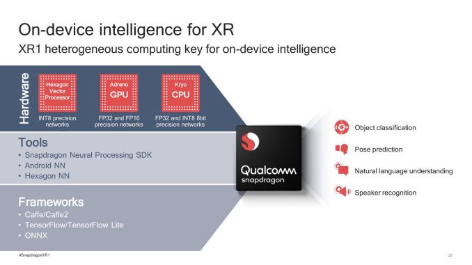
Which is not to say that the XR1 won’t be up to the challenge of rendered VR tasks either, as Qualcomm is clearly taking efforts to make that possible without blowing their power budget. But the current state of 3D rendered VR on mobile platforms is shaky, even on flagship-class SoCs. So similar to the Oculus Go or even some of the SD835-based headsets, rendered worlds are not going to be the strongest experience of these headsets.
As for AR, it remains to be seen. The company is promising a motion-to-photon latency of under 20ms, and the company’s Spectra ISPs are nothing to sneeze at. But these does stand to be the hardest market to break into, both for headset cost reasons and because it’s the least well developed in terms of consumer use cases. Not to mention VR-with-cameras will be going up against projected overlay technology ala Microsoft Hololens.
Wrapping things up, along with today’s product announcement, Qualcomm is also announcing that the XR1 is already near completion. The company has already signed on four partners for VR headsets, including not only frontrunner HTC Vive, but also Pico, Meta, and Vuzix, with the goal of not just shipping the XR1 SoC this year, but getting consumer headsets on the market by late this year. In which case we should be seeing designs from those partners very soon.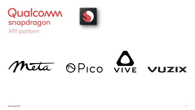
Gallery: Qualcomm XR1 Press Deck


More...
-
05-30-18, 07:16 AM #8187
Anandtech: The Supermicro X11SRA Motherboard Review: C422 based Workstation for Xeon-
For many professionals, a consumer level board may not have the features needed to satisfy their needs. Typically these boards include additional network functions and can have more and different types of storage options such as U.2 ports or switches. The Supermicro X11SRA, the motherbaord in this review, is aimed at the workstation market that sometimes has non-consumer demands. The X11SRA works only with the Xeon-W family of CPUs, analagous to the Skylake-X Core CPUs but supporting RDIMMs and ECC for up to 512GB of memy. These systems are designed to deliver a lot of horsepower, up to 18 cores, as well as storage and other needs.
More...
-
-
05-30-18, 11:45 AM #8189
Anandtech: Samsung Unveils 32 GB DDR4-2666 SO-DIMMs
Samsung on Wednesday introduced its first consumer products based on its 16 Gb DDR4 memory chips demonstrated earlier this year. The new SO-DIMMs are aimed at high-performance notebooks that benefit from both speed and capacity of memory modules.
Samsung’s new 32 GB DDR4 SO-DIMMs based on 16 Gb DDR4 memory ICs (integrated circuits) are rated for a 2666 MT/s data transfer rate at 1.2 V. Because the 16 Gb memory chips are made using Samsung’s 10 nm-class process technology, the new module is claimed to be 39% more energy efficient than the company’s previous-gen 16 GB SO-DIMM based on 20 nm-class ICs. According to Samsung, a laptop equipped with 64 GB of new memory consumes 4.578 W in active mode, whereas a notebook outfitted with 64 GB of previous-gen DDR4 consumes 7.456 W in active mode.
Samsung did not say when exactly it plans to start shipments of the 32 GB DDR4 SO-DIMMs. Meanwhile, DRAM producers usually make announcements after they ship the first batch of new products. Therefore, it is highly likely that Samsung’s customers among makers of high-end notebooks have already received the new 32 GB modules.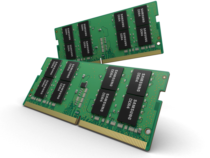
Samsung is gradually expanding its portfolio of 16 Gb (2 GB) memory chips for PC applications. Earlier this year the company introduced 16 Gb GDDR6 for graphics adapters and then demonstrated its server RDIMMs based on 16 Gb DDR4 chips. This week Samsung also mentioned 16 Gb GDDR5 chips for video cards.
Buy Samsung Galaxy S9 on Amazon.com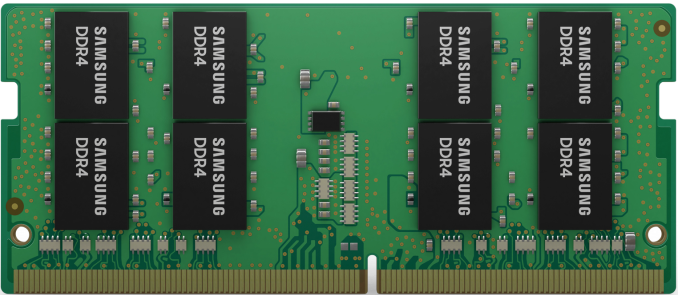
Related Reading- Samsung Demos 64 GB RDIMM Based on 16 Gb Chips, Promises 256 GB LRDIMMs
- Samsung Starts Production of 8 Gb DDR4-3600 ICs Using 2nd Gen 10nm-Class Tech
- Samsung Begins To Produce DDR4 Memory Using '10nm Class' Process Tech
- Samsung Starts Mass Production of 16Gb GDDR6 Memory ICs with 18 Gbps I/O Speed
More...
-
05-30-18, 01:35 PM #8190
Anandtech: Intel Launches Optane DIMMs Up To 512GB: Apache Pass Is Here!
Intel today announced the availability of their long-awaited Optane DIMMs, bringing 3D XPoint memory onto the DDR4 memory bus. The modules that have been known under the Apache Pass codename will be branded as Optane DC Persistent Memory, to contrast with Optane DC SSDs, and not to be confused with the consumer-oriented Optane Memory caching SSDs.
The new Optane DC Persistent Memory modules will be initially available in three capacities: 128GB, 256GB and 512GB per module. This implies that they are probably still based on the same 128Gb 3D XPoint memory dies used in all other Optane products so far. The modules are pin-compatible with standard DDR4 DIMMs and will be supported by the next generation of Intel's Xeon server platforms.
Gallery: Intel Optane DC Persistent Memory DIMMs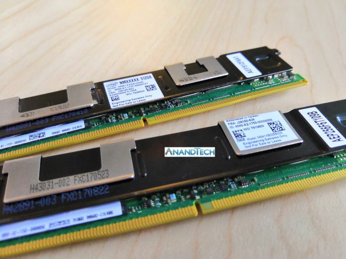


The Optane DC Persistent Memory modules Intel is currently showing off have heatspreaders covering the interesting bits, but they appear to feature ten packages of 3D XPoint memory. This suggests that the 512GB module features a raw capacity of 640GB and that Optane DC Persistent Memory DIMMs have twice the error correction overhead of ECC DRAM modules.
The Optane DC Persistent Memory modules are currently sampling and will be shipping for revenue later this year, but only to select customers. Broad availability is planned for 2019. In a similar strategy to how Intel brought Optane SSDs to market, Intel will be offering remote access to systems equipped with Optane DC Persistent Memory so that developers can prepare their software to make full use of the new memory. Intel is currently taking applications for access to this program.
Intel has been laying the groundwork for application-level persistent memory support for years through their open-source Persistent Memory Development Kit (PMDK) project, known until recently as NVM Library. This project implements the SNIA NVM Programming Model, an industry standard for the abstract interface between applications and operating systems that provide access to persistent memory. The PMDK project currently includes libraries to support several usage models, such as a transactional object store or log storage. These libraries build on top of existing DAX capabilities in Windows and Linux for direct memory-mapped access to files residing on persistent memory devices.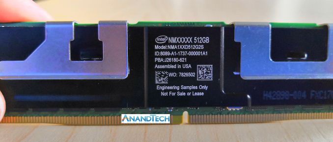
Optane SSD Endurance Boost
The existing enterprise Optane SSD DC P4800X initially launched with a write endurance rating of 30 drive writes per day (DWPD) for three years, and when it hit widespread availability Intel extended that to 30 DWPD for five years. Intel is now preparing to introduce new Optane SSDs with a 60 DWPD rating, still based on first-generation 3D XPoint memory. Another endurance rating increase isn't too surprising: Intel has been accumulating real-world reliability information about their 3D XPoint memory and they have been under some pressure from competition like Samsung's Z-NAND that also offers 30 DWPD with a more conventional flash-based memory.
This news is still in flux, so expect some more information later today.
More...


 Quote
QuoteThread Information
Users Browsing this Thread
There are currently 25 users browsing this thread. (0 members and 25 guests)


Bookmarks