

Results 8,381 to 8,390 of 12096
Thread: Anandtech News
-
07-13-18, 01:46 PM #8381
Anandtech: Cooler Master Releases CM310 Gaming Mouse: 10000 DPI Sensor, RGB Illuminat
Cooler Master has announced the release of a new gaming mouse in the CM310. The mouse includes a 10000 DPI gaming grade optical sensor, RGB illumination, and is designed to be ambidextrous. The new peripheral, according to Cooler Master, is designed as 'a mouse for gamers of all calibers and is designed to be comfortable, reliable, and doesn’t break the bank'.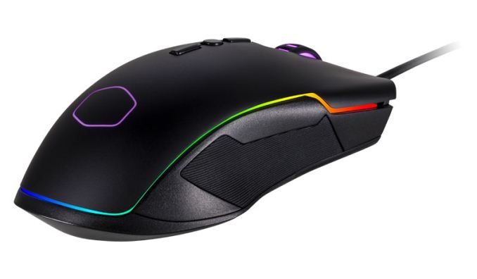
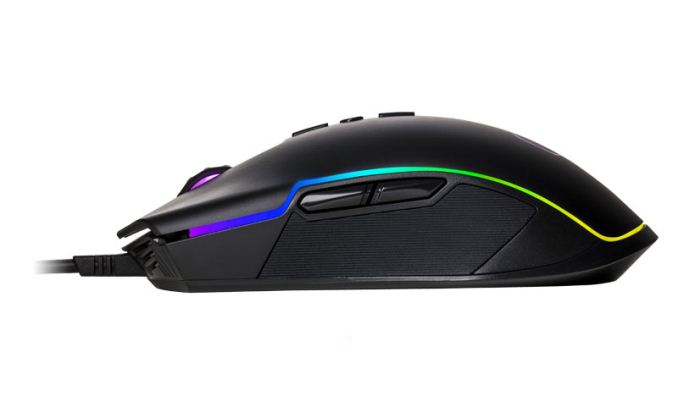
The outside of the mouse is made of a matte black plastic and rubber and includes an RGB illuminated web wheel. A Cooler Master symbol is on top, along with an RGB strip which is wrapped around the entire body. Cooler Master includes five preset RGB modes and effects, but no mention if it can work with motherboard RGB software. Although the mouse is said to be ambidextrous, the side buttons are on the left and for right-handed grip so this may not work as well for lefties who need those buttons. For increased grip, the sides of the mouse, where most users’ thumb and pinky finger rest, are rubberized to prevent slippage in the middle of a game.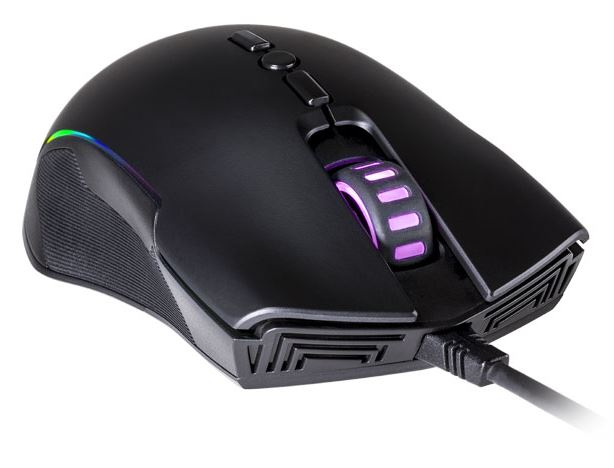
There are a total of eight buttons on the mouse. The three buttons on top are mapped to DPI changed and profiles for the ability to quickly switch to slower/faster movements on the fly with seven levels (500, 1000, 2000, 3000, 4000, 5000, and 10000 DPI). The remaining five buttons are the typical left and right we see on nearly every mouse, the two buttons on the left side along with the web wheel are also clickable.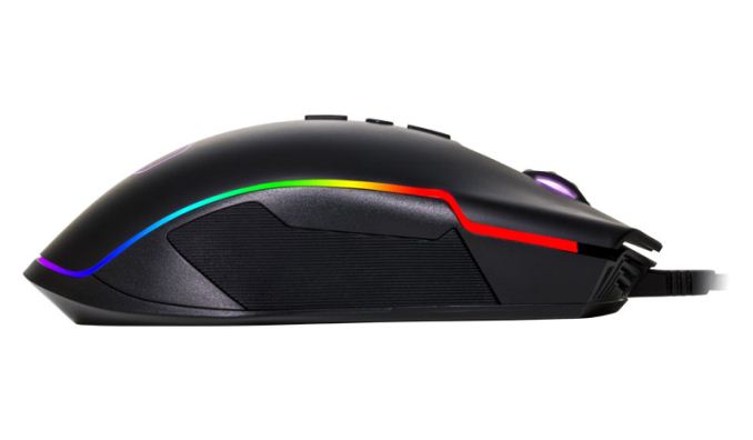
The device uses a Pixart A3325 sensor, good up to the 10000 DPI mentioned earlier, along with a polling rate of 1000 Hz, a lift-off distance of ~3mm, and uses a 60 inch-per-second tracking speed (3.4 miles per hour). The wired mouse uses a 6-foot USB 2.0 cable to connect to the PC.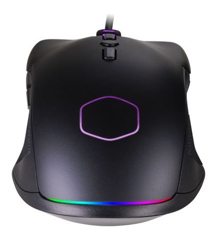
The Cooler Master CM310 is said to be available today at Newegg/Amazon and carries an MSRP of $30/30€.Cooler Master CM310 Gaming Mouse Product Name / Model # CM310 / CM-310-KKW02 Grip Type Palm & Claw Material ABS Plastic / Rubber Color Black LED Color 16.7M RGB with 5 Modes Sensor Pixart A3328 (10000 DPI) CPI / DPI 7 Levels (500, 1000, 2000, 3000, 4000, 5000, 10000) Tracking Speed 60 ips Lift Off Distance < ~3mm Polling Rate / Acceleration 1000 Hz / 20g Buttons 8 Connector / Cable Length USB 2.0 / 1.8 Meters (Flexible Rubber) Dimensions (W x H x D) 5" x 2.8" x 1.6" Weight 100g/135g (without/with cable) Warranty 2 Years
Related Reading- Azio Expands Lineup of 'Retro Classic' Perihperals with Mice, Pads, Palm Rests
- Alienware Releases Wirelss Headset and Elite Gaming Mouse
- ASUS ROG Gladius II Wireless Mouse
- Logitech Unveils G305 Mouse with Lightspeed Wiress, 'Hero' 12,000 DPI Sensor
More...
-
07-16-18, 10:28 AM #8382
Anandtech: An AnandTech Exclusive: The Jim Keller Interview
You asked for it, and we were able to get 30 minutes with the big man himself. Jim Keller falls into the rockstar category of engineers: lots of ideas with vision and a very successful record. Jim has been able to turn a product market around by leading processor design teams, such as with Apple's A4 and A5 processors, or AMD's K8 and Zen microarchitectures. Recently he was hired by Intel as the Senior Vice President of the Silicon Engineering Group, with an emphasis on SoC design and integration, although not much more was said, leaving everyone to scratch their heads as to exactly what projects fall under his remit. With Intel's money and design at his fingertips, we asked Jim what exactly his role now entails, how he is integrating into Intel, and what the plans are for the future.
More...
-
07-16-18, 10:28 AM #8383
Anandtech: NVIDIA Unifies GeForce NOW Service Across PCs and SHIELD TV STBs: 200+ Gam
NVIDIA this month is unifying its GeForce NOW service across all platforms that it supports, extending the latest iteration of the service for PCs and Macs to include NVIDIA's SHIELD TV consoles. From now on, all 225 games supported by the game streaming service will also run on the Android TV STB.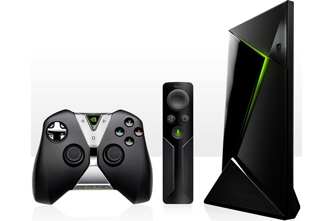
NVIDIA has been dabbling in cloud-based game streaming services for several year snow, starting with the GRID service early in this decade, which was created to extend the gaming capabilities of NVIDIA's first portable SHIELD devices. In October of 2015 this morphed into the first-generation GeForce NOW service, which was an interesting $8/month hybrid-subscription service that allowed users to both play games included with their subscription, along with buying certain (usually newer) games outright.
The service supported dozens of games that could be played using a gamepad, but omitted PC titles that required a keyboard and a mouse. Back then this limitation was conditioned by several factors: the service was new and NVIDIA needed streaming quality much more than it needed quantity of games, and availability of keyboards and mice supporting Google Android was scarce (and their universal compatibility was not guaranteed).
Meanwhile in early 2017 NVIDIA took the wraps off of its second-generation GeForce NOW service, which despite the identical name had a very different service model and an equally different (initial) audience. This seocnd-generation service was aimed PCs running macOS or Windows, and is currently operating as a free-to-use beta. Underpinning it is (or rather will be) the idea that rather than running a subscription service with a set library of games, NVIDIA would instead rent out compute time on virtual machines, with more powerful instances going for higher rates. Meanwhile users can bring their own games via access to their Steam, Uplay, and Battle.net accounts, getting NVIDIA out of the content curation game entirely.
Being aimed at computers with keyboards and mice, this version of the cloud-based game streaming service supported a considerably larger library of PC games. To date, the service on PCs/Macs has gained support for 225 titles, significantly higher than the number of titles available for the first-generation service for SHIELD devices.
Starting this month, however, the differentiation between services is coming to an end. NVIDIA is essentially discontinuing the first-generation GeForce NOW service, and in the process is moving SHIELD TV devices to the second-generation service. This will serve to unify GeForce NOW across all platforms, as now PC, Mac, and SHIELD TV will all access the same service.
Besides bringing SHIELD TV clients to technical parity with the PC, this change also means that SHIELD TV owners will be able to access all of the games that PC and Mac users can currently play. Obviously, to play RTS titles like Civilization V and VI (both are supported), SHIELD TV gamers will need to get a keyboard (and preferably a mouse) compatible with Google’s Android TV, but since this OS is rather widespread nowadays, this is hardly a problem (Logitech has several keyboards with touchpads for Android TV).
One thing to note about the service is that it is still in beta status. This is one of the reasons why it is free to use on PCs and now on SHIELD TV devices. It would seem that NVIDIA is still trying to figure out how to best monetize the service, so for at least throughout of 2018 users will continue to be able to access NVIDIA’s GeForce NOW streaming service for free.
Buy NVIDIA SHIELD TV on Amazon.com
Related Reading:
- NVIDIA Temporarily Slashes $30 Off the SHIELD TV: Now Staring at $149
- Google Assistant Released For NVIDIA's SHIELD TV; Other Vendors To Follow Shortly
- NVIDIA Launches SHIELD TV: Smart Home Functionality, More 4K HDR Streaming Services
- Google Assistant Released For NVIDIA's SHIELD TV; Other Vendors To Follow Shortly
- NVIDIA Releases Android 7.0 Update for 2015 SHIELD TV, Adds Amazon Video App
- NVIDIA SHIELD Android TV Console Adds Support for Vudu, HDR and 4Kp60 Content
More...
-
07-16-18, 01:59 PM #8384
Anandtech: ASRock Launches C246M WS Micro-ATX Motherboard for Xeon E CPUs
ASRock Rack has announced one of the industry’s first Micro-ATX motherboards for Intel’s new Xeon E processors for entry-level servers and workstations. The C246M WS platform is aimed at compact workstations, it supports a variety of PCIe add-in-cards, rather rich storage capabilities, and a couple of GbE connectors.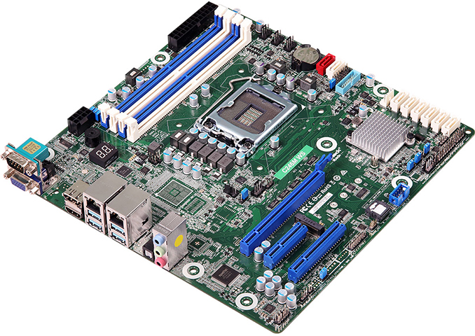
As the name suggests, the ASRock C246M WS motherboard is based on Intel’s C246 chipset and therefore supports Intel’s Xeon E-2100 series processors. The platform features a multi-phase VRM that uses solid-state inductors and capacitors to sustain stable operation during prolonged workloads. The design of the motherboard contains an empty pad for the Aspeed AST2500 IPMI chip, so eventually ASRock plans to launch a management version of the product as well. That server SKU will support IPMI 2.0 and will gain an additional Realtek RTL8211E Ethernet controller, the company’s website suggests. Probably for cost reduction reasons, the manufacturer decided not to install a TPM module onto its C246M WS workstation platform, but there is a TPM header, so the actual PC makers can still add this feature if their clients want it.
Just like other motherboards with the LGA1151 v2 socket, the C246M WS comes with four DDR4 DIMM slots supporting up to 64 GB of DDR4-2667 memory with ECC technology when a Xeon E processor is installed. PCIe 3.0 slots include one x16, one x8, and one x4 slot. The first one automatically switches to x8 mode once the second one is occupied.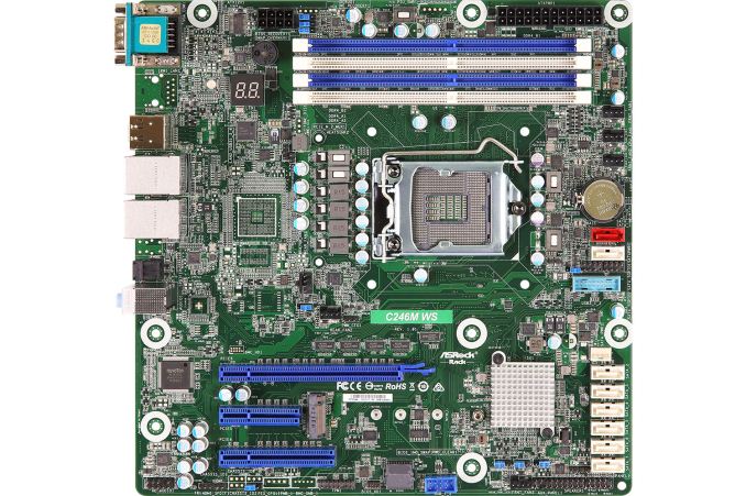
When it comes to storage, the C246M WS has one M.2 PCIe 3.0 x4 slot (supports both NVMe and SATA drives), and eight SATA connectors (one connector shares SATA with the M.2 slot, hence no more than eight SATA drives per system no matter the form-factor). If all storage options are used, the C246M WS can support up to 12 drives in a Micro ATX system: four PCIe/NVMe SSDs (one M.2 + three PCIe 3.0 slots) as well as eight SATA HDDs/SSDs.
Moving on to connectivity offered by ASRock’s C246M WS. The motherboard has two GbE ports, four USB 3.1 Gen 2 Type-A connectors (there are internal headers too), a D-Sub output (will be needed mostly on a server version outfitted with the AST2500 IPMI chip), an HDMI output, a Serial port, and audio outputs (analog and digital).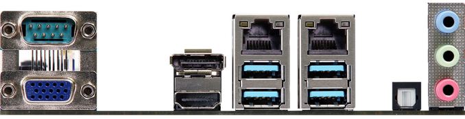
ASRock Rack generally sells products to businesses, so expect the C246M WS to show up inside entry-level compact workstations in the coming months. It is unclear when (if at all) the C246M WS emerges in retail and at what price point.ASRock's Micro ATX Motherboard
for Intel's Xeon E CPUsC246M WS Supported CPUs LGA1151 v2 CPUs
Xeon E 2100-seriesPCH Intel C246 Graphics Intel UHD Graphics from CPU
PCIe 3.0 x16 slotDisplay Outputs 1 × D-Sub
1 × HDMIMemory 2 × DDR4 DIMM
Up to 64 GB of DDR4-2667
ECC or non-ECCSlots for Add-In-Cards 1 × PCIe 3.0 x8
1 × PCIe 3.0 x4Ethernet LAN 1: Intel I219LM GbE PHY
LAN 2: Intel I210AT GbE PHYStorage 8 × SATA 6 Gbps (one SATA port is logically shared with M.2)
1 × M.2 (PCIe 3.0 x4 or SATA)Audio Multi-channel audio with 3.5-mm and S/P DIF outputs USB 4 × USB 3.1 Gen 2 Type-A
Internal headers for 2 USB 2.0 and 2 USB 3.0 portsSerial Ports 1 × RS232 Wi-Fi - Operating Temperature 10°C~35°C Form-Factor Micro ATX (244 mm × 244 mm | 9.6" × 9.6")
Related Reading- Intel Launches Coffee Lake Xeon E (Entry): The Next-Gen E3-1200
- iBASE Lists C246 Motherboards for Intel Xeon E CPUs
- Intel Xeon E3-1200 v7 Will Become Xeon Entry (Xeon E)
More...
-
07-16-18, 06:10 PM #8385
Anandtech: Intel and Micron To Dissolve 3D XPoint Partnership After 2019
A press release from Intel today has clarified the state of the 3D XPoint Joint Venture the company has with Micron. Currently Intel and Micron co-developed the new class of non-volatile memory, with manufacturing at the Intel-Micron Flash Technologies (IMFT) fab in Utah. Intel’s statement today states that for the second generation of memory, the development will also be a joint effort and is expected to complete in the first half of 2019. However the third generation will be developed independently, allowing each company to focus on the separate business needs.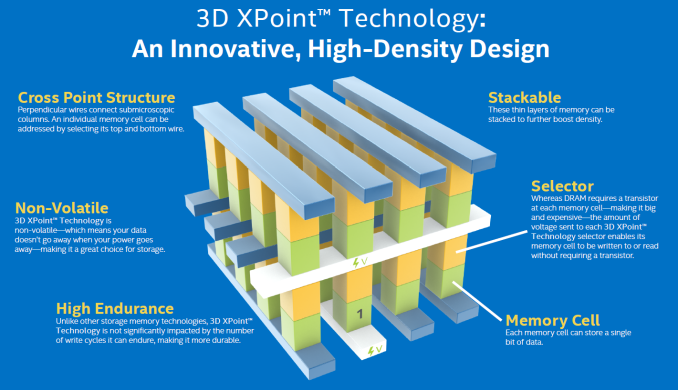
3D XPoint technology, branded as Optane by Intel and QuantX by Micron, has been a mini-revolution when it comes to non-volatile memory. Intel’s Optane products, mostly storage but with recent announcements about DRAM, have seen a sizeable uptick in interest from specific enterprise markets that can benefit from persistant data or fast random access storage. Intel is expected to launch its DRAM products alongside its next generation server architecture at some point in the new future. Under the terms of the joint venture, each company gets 50% of the flash memory made at the IMFT fab in Utah. Micron’s QuantX has not been released, which raises the question as to who has been buying it.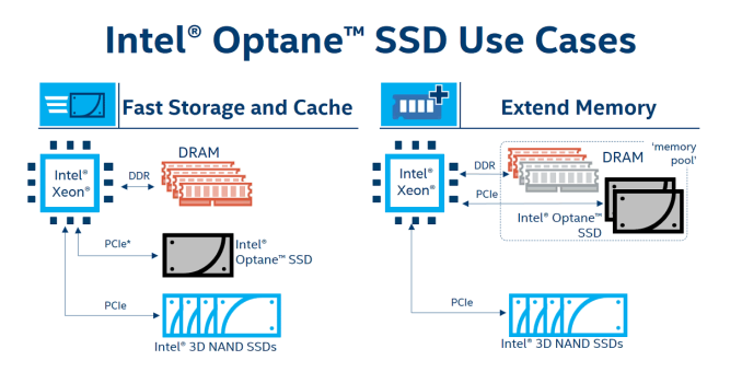
Intel has long held that 3D XPoint has a long life ahead of it, offering speed, density, and a wide range of applications. The industry is still waiting to be fully exposed to Intel’s initial promises about the product, from storage to memory, but also future generations of the product, such as adding layers and capacity. As with all technologies, these things are generational, and today’s announcement states that Intel and Micron are still working jointly with the second generation product. The completion of second generation 3D XPoint is expected in the first half of 2019, but then R&D focus will shift to completing and finalizing the third generation. It is this generation that is the focus of the announcement: the companies will no longer work together for it. This means that both companies will have a chance to adjust their roadmaps independently, either pursing a more aggressive strategy, or none at all. The note also states that the memory will continue to be built in the same fab, which raises questions as to how the joint venture will work in that case, if the research is done independently.
Both Intel and Micron have been having problems of late, with Intel’s Optane DRAM being released later than originally promised, and Micron having issues with the Chinese government, as well as disappointing sales of its own 3D XPoint. At least some clarity is being given to the 3D XPoint side of the businesses, if only to shine a light on the nature of the agreement for the next few years.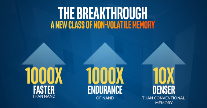
Related Reading- Intel Launches Optane DIMMs Up To 512GB: Apache Pass Is Here!
- Micron Update (Q2'18): 96L 3D NAND, Sales of 3D XPoint Disappoint
- The Intel Optane SSD DC P4800X (375GB) Review: Testing 3D XPoint Performance
- Micron Announces QuantX Branding For 3D XPoint Memory
- Analyzing Intel-Micron 3D XPoint: The Next Generation Non-Volatile Memory
Gallery: Intel and Micron Update 3D XPoint Roadmap: Combined Effort 2nd Gen, 3rd Gen Separate


More...
-
07-16-18, 06:51 PM #8386
Anandtech: Samsung Announces First LPDDR5 DRAM Chip, Targets 6.4Gbps Data Rates & 30%
Samsung has been on a roll lately with memory & storage-related announcements, and that roll is continuing today with a new DRAM-related announcement out of the juggernaut. This afternoon the company is announcing that they have completed fabrication, functional testing, and validation of a prototype 8Gbit LPDDR5 module. The company is targeting date rates up to 6.4Gbps-per-pin with the new memory, and while Samsung isn’t ready to start mass production quite yet, the company’s press release notes that they’re already eyeing it.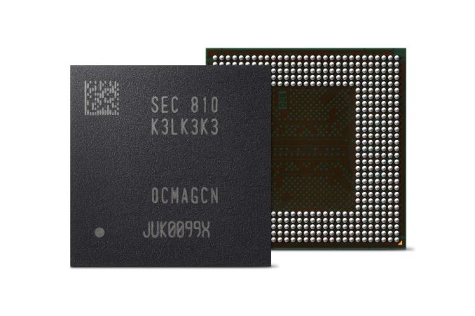
This is actually the first LPDDR5 announcement to cross AnandTech’s proverbial desk, so if you haven’t heard of the standard before, there’s a good reason for that. LPDDR5 is so cutting edge that the standard itself has yet to be completed; the JEDEC standards group has not yet finalized the specifications for DDR5 or LPDDR5. The JEDEC only first announced work on DDR5 last year, with the specification due at some point this year. As a result information on the memory technology has been limited, as while the major aspects of the technology would have been hammered out early, the committee and its members tend to favor holding back until the specification is at or is close to completion.
In any case, it appears that Samsung is the first to jump out of the gate on LPDDR5, becoming the first manufacturer to announce validation of their prototype. And as part of the process, they have revealed, at a high level, some important specifications and features of the new memory standard.
In terms of performance, Samsung is targeting up to 6.4Gbps/pin with the new memory. Which for a typical 32-bit bus chip works out to 25.6GB/sec of memory bandwidth. This is a 50% increase in bandwidth over the current LPDDR4(X) standard, which tops out at 4.266Gbps under the same conditions. So for a high-end phone where 64-bit memory buses are common, we’d be looking at over 50GB/sec of memory bandwidth, and over 100GB/sec for a standard 128-bit bus PC.
Underpinning these changes are a number of optimizations for both increased bandwidth and reduced power consumption. On the bandwidth side, the single biggest change is that the number of memory banks per channel, from 8 banks on LPDDR4(X) to 16 banks on LPDDR5. And while Samsung’s press release doesn’t explicitly note it – and I’m still waiting to get confirmation thereof – doubling the number of banks has traditionally gone hand-in-hand with doubling the prefetch size. This would give LPDDR5 a 32n prefetch size, with increasing the prefetch size long being the favored method to improve DRAM performance. Or to simplify matters a bit, the core clockspeed of the DRAM itself wouldn’t be changing, but rather LPDDR5 increases the amount of parallelism so that data is read and written out over more banks simultaneously.
Meanwhile for the memory bus itself, although not in Samsung’s own press release, we know from other sources that LPDDR5 is implementing differential clocking, similar to GDDR5 graphics memory. Differential clocking is key for a memory bus to be able to hit the high frequencies required to actually carry data in and out of DRAM as fast as LPDDR5 is going to be able to generate/consume it. Unlike the DRAM cells themselves, the memory bus can’t easily be made more parallel due to architecture and engineering limitations, so going faster is the only way forward without more radical changes. With that said, it’s known that differential clocking is responsible for GDDR5’s relatively high power consumption, so I’m curious what Samsung and the JEDEC have done to tamper this down.
And speaking of power consumption, let’s talk about the optimizations there. While LPDDR4X already jumped the gun here a bit by reducing the Vddq I/O voltage from 1.1v to 0.6v, LPDDR5 is implementing some of the other changes that have previously been proposed for future LPDDR standards. Voltages have once again been reduced, although Samsung isn’t listing what the new voltages are. Though presumably other voltages likes Vtt have been reduced this time around. Meanwhile Samsung’s press release also notes that the standard has introduced a feature to avoid overwriting cells already containing a 0, thereby avoiding wasting power to set the cell to 0 again.
Though from Samsung’s perspective the marquee feature in terms of power consumption savings on LPDDR5 is the new deep sleep mode. LPDDR5’s DSM is a longer sleep mode than what’s currently used in LPDDR4(X), allowing the DRAM to idle at even lower levels of power consumption. The tradeoff I expect being that it takes longer to enter and exit this sleep mode, based on how deep sleep modes make similar tradeoffs in other devices. Overall Samsung is claiming that this new sleep mode consumes have as much power as LPDDR4X’s idle mode. Ultimately the company estimates that due to the combination of these features, LPDDR5’s power consumption will be upwards of 30% lower than LPDDR4X, though it’s not clear whether this is total package power consumption or power consumed per bit of data moved.
Samsung for their part will be offering two speed/voltage grades of LPDDR5. Their fastest 6.4Gbps SKU will operate at 1.1v, and meanwhile they will also offer a 5.5Gbps SKU that runs at a lower-still 1.05v for devices that need even lower power consumption. And as mentioned earlier, Samsung has not yet begun mass production – presumably this can’t happen until the specification is formally ratified – but is eying to get mass production going soon.
Finally, like LPDDR4 before it, expect Samsung and other manufacturers to initially chase the mobile market with this new generation of memory. Samsung is officially stating that the memory is for use in "upcoming 5G and Artificial Intelligence (AI)-powered mobile applications,” and buzzwords aside, this is the mobile market in a nutshell. However since LPDDR5 will be a core JEDEC standard, as our own Dr. Ian Cutress was already asking me when Samsung sent over the announcement, it seems like it’s just a matter of time until LPDDR5 support comes to x86 processors as well. Though if LPDDR4 is any indication, “a matter of time” can still be quite a while.
More...
-
07-17-18, 08:48 AM #8387
Anandtech: VirtualLink USB-C Alt Mode Announced: Standardized Connector for VR Headse
While PC VR headsets are fun, no one has especially enjoyed the number of cables required to hook one up. With separate video, power, and data cables, the end result has been that manufacturers have used somewhat unwieldy cables or breakout boxes. However as part of the generalized push towards the second generation of VR headsets, a new industry consortium is coming together today to reduce the requirements to a single cable. Backed by NVIDIA, AMD, Oculus, Valve, and Microsoft, the new VirtualLink standard is a USB Type-C alternate mode that will be able to supply all of the necessary power, video information, and data over a single Type-C cable and connector.
Today’s announcement from the group is essentially a call for participation, announcing the group’s existence and inviting others to get involved ahead of the VirtualLink 1.0 specification. So the consortium and its members are broadly talking about the standard itself, but are not saying anything about products that may implement it. And indeed as of Monday evening as I’m writing up this article, the VirtualLink consortium’s website still isn’t up.
In any case, the rationale for creating a standardized connector is pretty straightforward. A clunky multi-port cable is okay for first-generation early adopter products, but if the consortium members want to push VR adoption, then the setup process needs to be easier to reach the masses. This includes not only reducing the cable down to a single port, but also making these headsets easier to use with laptops, where HDMI ports are uncommon and DisplayPort is primarily picking up penetration through the popularity of the associated USB-C alternate mode. So a standard for a single cable, using the smallest yet most compatible port choice, is going to be the best way forward.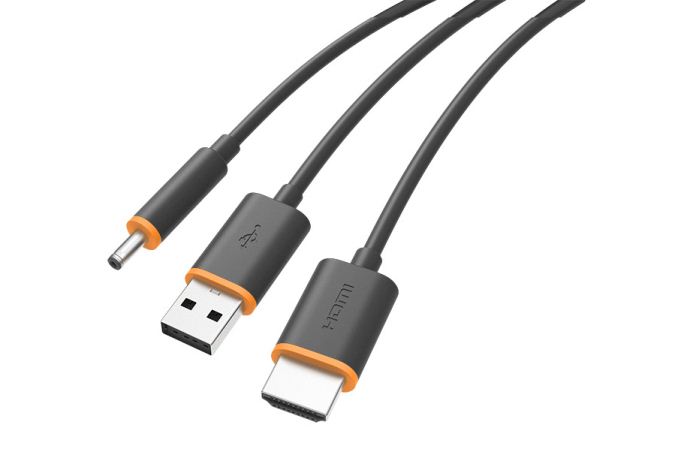
HTC Vive Cable Set
What this amounts to is that the standard is being implemented as a USB Type-C alternate mode. USB-C is the natural choice here, as the wider industry is already consolidating around the port for external connectivity, and the port + cable is designed to carry multiple lanes of data along with significant amounts of power. In fact I was a bit surprised that this required a new alternate mode at all – we already have the DisplayPort alternate mode – but after checking with the consortium, there is a good reason for this.
The official VirtualLink standard calls for 6 lanes of high speed data – 4 DisplayPort HBR 3 channels for video, and a single USB 3.1 Gen 2 channel (2 lanes) for data – along with 27W of power. And while you can combine the DisplayPort alt mode with those power requirements, the lynchpin is 4 lanes of video plus the USB 3.1 Gen 2 data channel. By the standard, DisplayPort alt mode replaces all of the USB 3.1 data channels, leaving only the much slower USB 2.0 baseline channels available.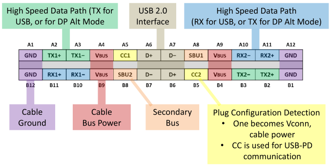
As it turns out, tucked away in version 1.3 of the USB Type-C cable specification released last year, the USB-IF has made some small but important changes to what alternate modes are allowed to do, which in turn means that new standards are needed to take advantage of these changes. In short, for direct connect devices – that is, devices connected directly to a USB-C port and not going through a hub or other extender/repeater – those devices are now allowed to reconfigure the 4 USB 2.0 pins (A6/A7/B6/B7) after the device handshake. So for the VirtualLink standard, this means that VR headsets can tap these additional 4 pins, giving them the extra flexibility they need in order to simultaneously meet the video, power, and date requirements of a VR headset.USB Type-C Alternate Modes VirtualLink DisplayPort
(4 Lanes)DisplayPort
(2 Lanes)Base USB-C Video Bandwidth (Raw) 32.4Gbps 32.4Gbps 16.2Gbps N/A USB 3.x Data Bandwidth 10Gbps N/A 10Gbps 10Gbps + 10Gbps High Speed Lane Pairs 6 4 Max Power 27W
(Mandatory)Up To 100W (Optional, depending on manufacturer)
Diving a bit deeper, what this essentially means is that the 4 USB 2.0 pins have been turned into another pair of high-speed differential lanes, giving compliant USB-C connectors 6 high-speed lanes overall. Normally these 4 pins are implemented in a USB-C cable as simple unshielded twisted pairs, which is sufficient for USB 2.0 data. However high-speed operation requires shielded differential pairs, which is not part of the base cable specification. But in the case of direct connect devices, they come with their own cable, meaning the usual cable rules can be thrown out the window and vendors can specifically use higher quality cabling to get away with high speed data on these pins.
The net result of all of this is that the VirtualLink standard is a rather forward-looking standard in terms of capabilities. 4 lanes of HBR3 video data alone is equivalent to a DisplayPort 1.4 connector, which is to say that it offers enough video bandwidth for 4K @ 120Hz with 8bpc color. This is more than double the bandwidth afforded to the Rift and Vive via their HDMI 1.3 connectors. I also find it interesting that after favoring HDMI for the first-generation products, this change means the industry is shifting to DisplayPort. DisplayPort of course is royalty free, among its other advantages, however its packet-based data transfer paradigm is very different than HDMI’s classic pixel-based TMDS system, which is an important distinction when you’re talking about how to best fight latency.
Meanwhile a full USB 3.1 Gen 2 data connection means there’s 10Gbps of bandwidth for data transfers between HMDs and the host computer, which right now at least is bordering on overkill. Though I’m very curious what the consortium is doing here (if they’re doing anything at all) to combat the fact that USB 3.1 Gen 2 data is normally only rated to run over 1 meter cables due to faster signal attenuation, which is a rather short cable length for a VR headset and the room scale experiences the vendors are pushing. Otherwise the 27W power standard sounds high at first as well, but it’s a sensible choice. The current Vive and Rift consume a fraction of that, but they had to be designed around the limitations of a USB 3.0 Type-A connector to begin with. As headsets become increasingly powerful in their own right – especially with inside-out tracking – a greater power budget will undoubtedly come in handy. As an aside, the consortium’s announcement doesn’t list voltages here, but 27W is almost certainly 9V @ 3A, a common mid-power point for USB-C devices.
Unfortunately this is the limit to what we know about the specification at this time. As mentioned previously, the consortium’s members aren’t talking about specific implementations quite yet, such as which types of devices the members would like to put VirtualLink-capable USB-C ports on. For desktop PCs the logical choice is video cards – especially if USB-C eventually replaces the DisplayPort connector outright – which is something we’ve seen manufacturers toy with, but not actually reach shipping products. This would also be consistent with the consortium’s goals of making VirtualLink a low-latency port (owing to the comfort requirements for VR).
The flip side to all of this is that AMD, NVIDIA, and their board partners would need to start implementing either USB 3.1 controllers or USB 3.1 headers on their cards, in order to supply the necessary data connectivity. Which is not too difficult to do, but it’s yet another feature that video cards would need to support. And without going too far down the rabbit hole here, where this ultimately could lead to is that we’re about to see a major shift in the kinds of ports available on video cards, especially if most video cards need to be VirtualLink capable to maximize the number of systems that can be used with VR headsets.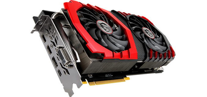
MSI's Unreleased USB-C Equipped GTX 1080 Ti
Conversely, laptops should be relatively easy due to their highly integrated nature. USB-C ports are already common there, so it’s just a matter of adding another USB-C alternate mode. However it does call into question whether the consortium will be able to convince laptop manufacturers to adopt the alt mode for large swaths of their product lines (similar to the DP alt mode today), or if it will only be found on high-end gamer-focused laptops.
In any case, this should be a welcome development for the industry as a whole. While VR hasn’t proven to be as immensely popular with consumers as some vendors had hoped, VR headset adoption has shown solid growth and spurred plenty of system upgrades to drive the data-hungry headsets. So anything that further simplifies the process is going to be a welcome move for consumers and hardware vendors alike.
More...
-
07-17-18, 08:48 AM #8388
Anandtech: MediaTek Launches Helio A Series SoCs, Starting With Helio A22
Following the success of their Helio P and X series SoCs, MediaTek this morning is announcing a third SoC family to complement the existing pats: the Helio A series. Aimed at what MediaTek is calling the “mid-market”, the new “Advanced” series of SoCs is meant to address phones in the $100+ range, which would put it in competition with the likes of Qualcomm’s Snapdragon 400 series. Kicking off the Helio A series family in turn is the A22, essentially MediaTek’s cheaper downmarket counterpart to the previously announced P22.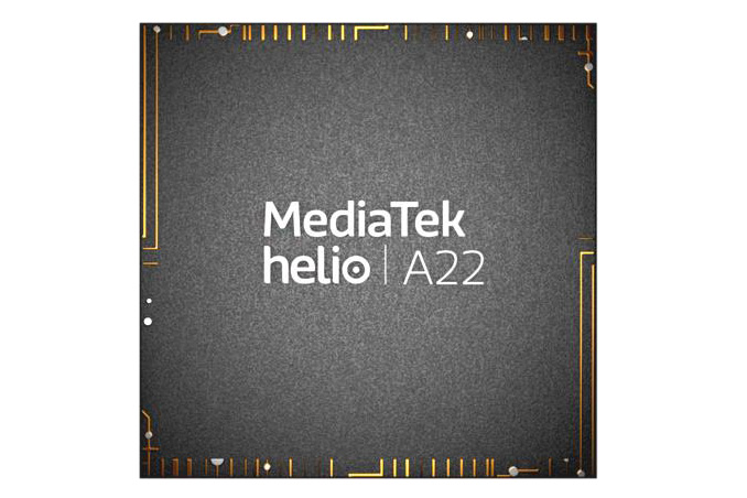
MediaTek is of course no stranger to the entry-level market, the “mid-market”, or whatever else it may be called. While flagship phones and their equally flagship SoCs get most of the attention, it’s the entry-level market where the volume play is. And this goes for both western markets where smartphones are already established, as well as emerging markets where smartphone penetration is still growing. So it’s a market that MediaTek is keen to continue addressing, and to continue to fend off other competitors.
Today the company is just announcing the first SoC for the A series family, though as the A22 is a relatively straightforward entry-level SoC, I wouldn’t be too surprised if this part is towards the low-end of the product stack going forward. Officially in their larger product stacks and promotional materials, MediaTek is lumping the A series more alongside parts such as the MT6750 – an octa-core Cortex-A53 based part – whereas the A22 is a simpler quad-core A53 design. So in practice, the Helio A22 is more a successor towards the MT6738/MT6739, which were also quad-core designs. Though lines of succession aside, it’s clear that the ultimate goal here for the company is to phase out the high-level use of MTxxxx product numbers, which would be a welcome development as the X/P/A series messaging is a lot clearer about which market and performance segments an SoC is meant to fit in.
In any case, let’s dive in to the Helio A22 itself. As previously mentioned, the A22 is built around a quad-core Cortex-A53 CPU cluster, which in this latest SoC will be clocking at up to 2GHz. Those CPU cores will in turn be paired up with an Imagination PowerVR GE8320 GPU, a single cluster GPU design released by Imagination last year. Overall this is relatively similar to the MT6739, following the same CPU and GPU architectures but with more powerful configurations chosen. However beyond that, the AA immediately starts setting itself apart from the MT6739 thanks to its manufacturing process: it is the first entry-level MediaTek SoC to be produced on a sub-28nm process, with MediaTek specifically using TSMC’s 12nm process, the same used for the Helio P60.
MediaTek isn’t especially promoting the use of TSMC’s 12nm process, but the choice is none the less an important one. The most immediate benefit to users are the power savings MediaTek will see from the newer process; the company expects to very well here thanks to the process and what they feel is a market-leading power & task management technology in the form of the latest CorePilot, As for OEMs, the benefit of the smaller 12nm is just that: it’s smaller. And since die size is king in the entry-level market, it means that the A22 stands to be a very competitive chip indeed, maximizing the number of chips produced per wafer and keeping SoC costs to a minimum.MediaTek Entry-Level SoCs SoC Helio A22 MT6739 MT6738 CPU 4x Cortex A53 @ 2.0GHz 4x Cortex A53 @ 1.5GHz 4x Cortex A53 @ 1.5GHz GPU IMG PowerVR GE8320 IMG PowerVR GE8100 @ 570MHz Mali T860 MP2 @ 350MHz Memory 1x 32bit LPDDR3
@ 933MHz
2x 16bit LPDDR4X @1600MHz1x 32bit LPDDR3 @ 667MHz 1x 32bit LPDDR3 @ 667MHz ISP/Camera 13 + 8 MP or 21MP 13MP 13MP Encode/
Decode1080p30 H.264 1080p30 H.264 1080p30 H.264 Integrated Modem Category 7/13
Dual-SIM
DL = 300Mbps
UL = 150MbpsCategory 4/5
Dual-SIM
DL = 150Mbps
UL = 50MbpsCategory 6
DL = 300Mbps
UL = 50MbpsWireless 802.11ac + BT 5.0 802.11n + BT 4.2 802.11n + BT 4.2 Mfc. Process TSMC 12nm 28nm 28nm
Overall however, MediaTek’s strongest focus on the SoC isn’t on its core configuration of performance; as should be obvious from the core specifications of the phone, the SoC isn’t going to burn up the charts in terms of performance. Rather the company is trying to differentiate itself and the A22 from a feature standpoint, particularly in the areas of camera support and LTE performance.
On the camera side of matters, the entry-level SoC will sport two ISPs, allowing the phone to drive two cameras simultaneously. By the numbers, this will allow for a 13MP + 8MP camera configuration, or a single camera can go up to 21 MP. Arguably this choice is more focused on still photography than videos, as the dual camera setup favors the former – it’s difficult to argue with the popularity of artificial bokeh in consumer photos. The SoC’s fairly modest video encode block, by comparison, tops out at just 1080p30, so it affords relatively basic video recording.
As for cellular networking performance, the A22 will support LTE Category 7 downloads and Category 13 uploads, allowing for download rates upwards of 300Mbps and upload rates of 150Mbps. And as one might expect for an entry-level SoC, the A22 is a dual-SIM product, supporting VoLTE on both networks. This has been a recurring feature push by MediaTek as they believe the second SIM should offer feature parity with the primary SIM, especially as some of the expanding markets they’re now going after were built for LTE from the start, meaning that those markets have limited 3G/2G connectivity.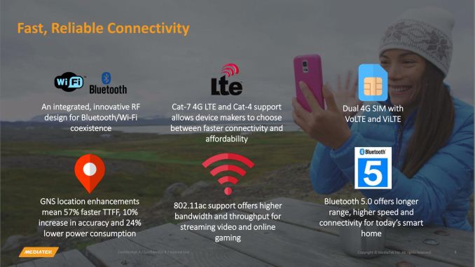
And while it doesn’t get a separate product number, MediaTek will be offering a second, cheaper version of the A22 SoC with more limited LTE Category 4 support. As one might expect, the Cat 4 model is for cost reasons; besides being a cheaper chip, Cat 4 doesn’t require carrier aggregation like Cat 7 does, allowing for simpler radios that don’t need to be able to tune and bond multiple bands at once, ultimately resulting in cheaper phones.
Finally, expect to see MediaTek and its OEM customers throwing AI around a lot, as AI functionality continues to be a buzzword in the market. In the case of the A22 the SoC does not have any dedicated neural networking hardware – there isn’t an NPU here like in the P60 – so those are executed on the GPU and the CPU as necessary. MediaTek is however providing the necessary drivers to and infrastructure to support Android’s NNAPI, so programs built against the API will be able to use the GPU (relatively) transparently, and this is where MediaTek’s claims for AI support come from.
Wrapping things up, the Helio A22 SoC is already shipping today; and indeed phones based on the SoC are already shipping as well. Xiaomi’s Redmi 6A is already out in China, with additional phones to follow. The 6A is, in turn, running for around $110 USD, which should give you a solid idea of the market segment MediaTek is chasing with the A22.
Gallery: Helio A22 Press Deck


More...
-
07-17-18, 10:46 AM #8389
Anandtech: The ASUS X399 ROG Zenith Extreme Motherboard Review: Top Tier Threadripper
Today we are having a look at the most expensive motherboard for Ryzen Threadripper processors, the ASUS X399 ROG Zenith Extreme. The motherboard has a very impressive list of features that reach far beyond what a consumer expects to see on a regular product, such as hardware support for liquid nitrogen cooling. We will closely inspect the motherboard and its features in this review.
More...
-
07-17-18, 12:29 PM #8390
Anandtech: NZXT Enters PSU Market with E-Series ATX Power Supplies Featuring Built-In
NZXT has been expanding at a quite rapid pace in the recent years. Back in 2017 the company introduced its first motherboard and today it is launching its first PSUs. The NZXT E-series power supplies are made by Seasonic and support active monitoring of power consumption across the 12 V rail as well as temperature, which are their key features.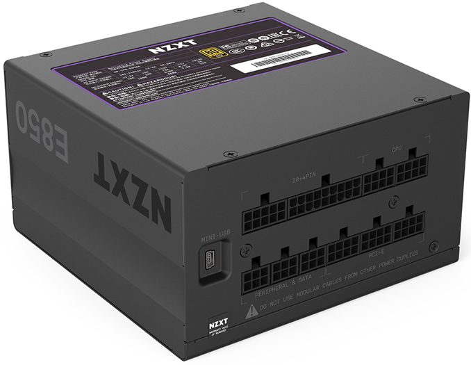
The NZXT E-series PSUs are based on Seasonic’s Focus+ Gold platform featuring the PMBus architecture. The lineup includes three modular power supplies compliant with the latest ATX specification and rated for 500, 650, and 850-Watt output. Just like many other advanced PSUs, the new NZXT power suppliers use Japanese capacitors that can handle temperatures of up to 105°C as well as support overcurrent protection for the 12 V rail. Furthermore, the new PSUs also carry the 80 Plus Gold badge.
One of the key selling points of the NZXT E-series PSUs is built-in wattage monitoring for the 12 V rail. The monitoring is handled by the company’s CAM software, which works only with Windows 10 operating system. In addition to monitoring power consumption, the CAM application can also manage rotating speed of fans and activate Silent, Performance, or Fixed preset modes.
NZXT’s E-series PSUs are now available from the company’s website in the U.S. NZXT’s partners on Europe and other countries will start selling the new power supplies starting in late July. As for pricing, the most affordable NZXT E500 PSU costs $125, whereas the most powerful model rated for 850W is available for $150. Meanwhile the 650-W model is priced at $135. All the new PSUs are backed with a 10-year warranty (just like Seasonic’s Focus+ Gold), which is a rare feature for relatively inexpensive power supplies.NZXT E-Series PSUs Output Specifications 500 W 650 W 850W Rated Combined Rated Combined Rated Combined +3.3V 20 A 100 W 20 A 100 W 20 A 100 W +5V 20 A 20 A 20 A +12V 41 A 492 W 54 A 648 W 70 A 840 W -12V 0.3 A 3.6 W 0.3 A 3.6 W 0.3 A 3.6 W +5Vsb 3 A 15 W 3 A 15 W 3 A 15 W Total Power 500 W 650 W 850 W
Related Reading:NZXT E-Series PSUs Connectivity Specifications Connector type 500 W 650 W 850 W ATX 24 Pin 1 EPS 4+4 Pin 1 2 EPS 8 Pin - PCIe 6+2 Pin 2 4 SATA 8 4P Molex 3 6 Floppy -
- NZXT Expands Kraken AIO Lineup: Their First 360mm AIO, New Kraken M Series
- The NZXT N7 Z370 Motherboard Review: A New Player in the Motherboard Market
- NZXT Releases Kraken G12 Liquid Cooler GPU Mounting Kit
- NZXT Unveils Fully Customizable Aer RGB LED Fans
More...


 Quote
QuoteThread Information
Users Browsing this Thread
There are currently 12 users browsing this thread. (0 members and 12 guests)


Bookmarks