

Results 8,411 to 8,420 of 12096
Thread: Anandtech News
-
07-25-18, 12:26 PM #8411
Anandtech: Samsung Discloses First Details About QLC-Based Client & Server SSDs
It is not a secret that Samsung deliberately avoided QLC NAND with its 64-layer V-NAND flash, in the process citing various reasons. With its 96-layer V-NAND however, the company is changing its approach and is going to offer QLC-based SSDs for client and server computers. At the Samsung SSD Forum in Japan the company disclosed the first details about the upcoming drives.
The key advantage of 3D QLC NAND over 3D TLC is of course a 33% higher storage density and therefore a lower per-bit storage cost (assuming a similar yield). Therefore, the first drives to adopt Samsung’s 3D QLC V-NAND will be high-capacity SSDs for those customers who need to store a lot of data and may not be that interested in the maximum performance.
Samsung has been openly working on ultra-high-capacity SAS/U.2 SSDs based on QLC V-NAND memory for well over a year now. These drives will be used for WORM (write once, read many) applications not optimized for fast writes, but clearly outperforming HDD-based arrays. Samsung expects its first QLC-powered NVMe drives to offer up to 2500 MB/s sequential read speed as well as up to 160K random read IOPS, significantly outperforming high-end 10K RPM HDDs. Evidently, high-capacity QLC-based SSDs are supposed to substitute multiple 10K RPM hard drives working in a RAID array, so comparing performance of a single SSD to a 2.4 TB HDD may not be too representative, especially when power consumption is taken into account.
Another lineup of Samsung’s products to use 3D QLC V-NAND will be client SSDs featuring capacities higher than 1 TB. These drives will use a SATA interface and will offer sequential read and write performance of around 520 MB/s (when SLC write caching is enabled), according to details that Samsung disclosed at its SSD Forum. Samsung does not disclose when such drives are set to become available, but the company says that Terabyte-class client SSDs will become mainstream in 2020 because of QLC V-NAND.
In the meantime, Samsung does not expect QLC V-NAND to replace TLC V-NAND as the mainstream type of flash memory any time soon. QLC NAND requires more expensive controllers with considerably higher processing capabilities to guarantee a proper endurance. Therefore, the low-cost per-bit advantages of memory may not be that obvious on client SSDs.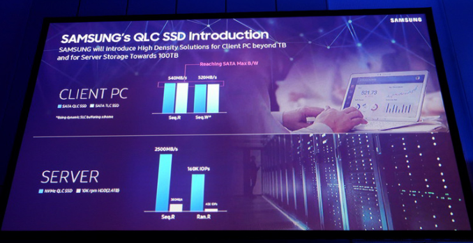
Related Reading:
- Samsung Begins Mass Production Of 96L 3D NAND
- Western Digital Begins to Sample QLC BiCS4: 1.33 Tbit 96-Layer 3D NAND
- Intel Teases Upcoming QLC SSD For Datacenters
- We Found a Prototype 4 TB Intel QLC SSD
- Intel QLC NAND Updates: Up to 20TB In 2.5-inch SSD
- Intel And Micron Launch First QLC NAND: Micron 5210 ION Enterprise SATA SSD
- Toshiba's 768Gb 3D QLC NAND Flash Memory: Matching TLC at 1000 P/E Cycles?
More...
-
07-25-18, 12:26 PM #8412
Anandtech: The ADATA XPG SX8200 & GAMMIX S11 NVMe SSD Review: High Performance At All
With the ADATA XPG SX8200 and the related XPG GAMMIX S11, ADATA has moved past the performance limitations of their earlier NVMe SSDs and finally delivered high-end drives at competitive prices. Thanks to the latest Silicon Motion NVMe controller and Micron 64-layer 3D TLC NAND, these drives offer great performance across the entire capacity range.
More...
-
07-25-18, 02:39 PM #8413
Anandtech: Intels Xeon Scalable Roadmap Leaks: Cooper Lake-SP, Ice Lake-SP Due in 20
Recently a Chinese university has published a collection of slide-decks from various companies covering a server/HPC event. Among the slides, Intel had a seemingly longer comprehensive presentation describing Intel’s conceptual approaches to HPC to analysis of various workloads, and most interestingly, future plans and what looks to be an up-to-date server roadmap.
According to slides published by the Central South University from Changsha City, Hunan, Intel had to delay its Ice Lake-SP server platform from 2019 to 2020 because of the general delay of its 10 nm process technology. What was unknown and newly revealed in the roadmap, is that in addition to the codenamed Ice Lake-SP processors, the company is also preparing the codenamed Cooper Lake-SP CPUs that are set to arrive a bit ahead of the Ice Lake-SP chips. The document was demonstrated to students and professors by Intel itself at a special server/HPC event earlier this month.
Both Cooper Lake-SP and Ice Lake-SP processors will support the codenamed Barlow Pass DIMMs, which is most probably Intel’s next-generation Optane DC Persistent Memory DIMM running next-gen 3D XPoint non-volatile memory (though it is a speculation at this point). Intel does not disclose the difference between the Cooper Lake-SP and the Ice Lake-SP products, but it is possible that the former is the company’s “Plan B” for next-generation servers should anything happen with its 10 nm process technology or the ICL-SP design. Meanwhile, both Cooper Lake-SP and Ice Lake-SP will belong to one server platform that will also support an eight-channel per-socket memory sub-system along with multiple OmniPath fabric innovations.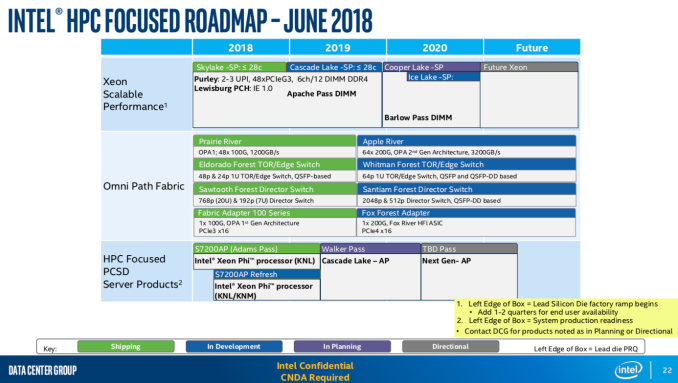
Intel expects to begin production ramp of its Cooper Lake-SP CPUs in late 2019 or early 2020 with end user availability in late Q1 2020 or mid-2020. By contrast, the Ice Lake-SP will start their ramp sometimes in late Q1 2020 and will be available in Q3 or Q4 of 2020.
Another interesting thing to point out in Intel’s roadmap is that the company is prepping the codenamed Walker Pass platform and the codenamed Cascade Lake-AP processor for the HPC market segment. The aforementioned CPU is said to replace the Xeon Phi 7200-series “Knights Landing” processor for technical computing. Meanwhile, as the name suggests, the Cascade Lake-AP will heavily rely on Skylake SP-based design for mainstream servers.
Intel traditionally does not comment on information obtained unofficially and therefore we cannot find out how accurate the current roadmap is.
Related Reading:
- Power Stamp Alliance Exposes Ice Lake Xeon Details: LGA4189 and 8-Channel Memory
- Intel’s High-End Cascade Lake CPUs to Support 3.84 TB of Memory Per Socket
- Intel Documents Point to AVX-512 Support for Cannon Lake Consumer CPUs
- Intel Begins EOL Plan for Xeon Phi 7200-Series ‘Knights Landing’ Host Processors
- Intel Shows Xeon Scalable Gold 6138P with Integrated FPGA, Shipping to Vendors
- Sizing Up Servers: Intel's Skylake-SP Xeon versus AMD's EPYC 7000 - The Server CPU Battle of the Decade?
Via: Twitter / David Shor
More...
-
07-25-18, 02:39 PM #8414
Anandtech: Intel Provides Royalty-Free License for Data Bus to DARPAs Modular Chips
Taking place this week is DARPA’s 2018 Electronic Resurgence Initiative (ERI) Summit, the defense research agency's first gathering to address the direction of US technology manufacturing as Moore's Law slows down, and how the agency can jumpstart alternative efforts to ensure continued performance scaling. To that end, in an interesting and unexpected move from the summit, Intel has announced that it would offer a royalty-free license for its Advanced Interface Bus (AIB) to participants of the agency’s Common Heterogeneous Integration and Intellectual Property (IP) Reuse Strategies (CHIPS) program. The move will help interested parties to design SoCs utilising heterogeneous components made using different process technologies.
Modern, complex chips are hard to manufacture and equally hard to design, as they frequently contain a number of different application-specific functional blocks (e.g., general-purpose cores, graphics cores, etc.). In a bid to somehow reduce costs of chip design, numerous companies have come up with modular development approaches that allow them to design SoCs using more or less standard components. This methodology is used to develop modern SoCs for mobiles, game consoles, and other consumer electronics. However, it is largely believed that the approach is still not enough cost-effective for future SoCs, as the entire chip must still be manufactured as a single, monolithic die. As a result, Intel has propose using so-called chiplets, which are heterogeneous components of a chip produced using different process technologies and interconnected using its AIB interface.
Intel’s Advanced Interface Bus is a low-power die-to-die interface that is based on a forward clock parallel I/O architecture. AIB features a 1 Gbps per lane SDR transfer rate for control signals and a 2 Gbps per lane DDR transer for data. AIB is agnostic to particular packaging technology used: it can rely on Intel’s own EMIB, or can use other packaging technologies (e.g., CoWoS, InFO, etc.) too. Intel itself of course uses its AIB for its Stratix 10 FPGAs (more on this here), but since the tech is universal, participants of the CHIPS program will be able to use the interface for whatever projects they are working on.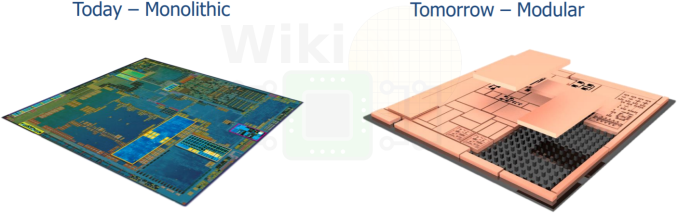
The whole idea behind the CHIPS initiative is to enable developers of SoCs to re-use existing semiconductor blocks for future projects, and to only build blocks on the smallest/most powerful (read: expensive) manufacturing process that part requires. Intel itself proposes to use 10-nm CPU and GPU cores along with communication blocks produced using a 14 nm fabrication process, as well as other components made using a 22 nm manufacturing tech. For developers who do not have access for Intel’s technologies and who have considerably lower R&D budgets, it will make sense to re-use some of the IP produced using a planar fabrication process with processing cores made using a leading-edge FinFET technology.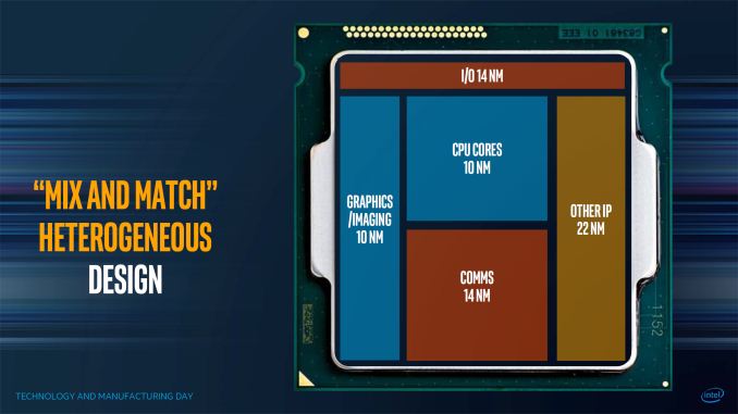
It remains to be seen when participants of DARPA’s CHIPS program actually start to use Intel’s AIB, but the fact that they now have a technology that could wed leading-edge IP with proven blocks looks rather promising.
Related Reading:
- Intel Launches Stratix 10 TX: Leveraging EMIB with 58G Transceivers
- Intel to Create new 8th Generation CPUs with AMD Radeon Graphics with HBM2 using EMIB
- Hot Chips: Intel EMIB and 14nm Stratix 10 FPGA Live Blog (8:45am PT, 3:45pm UTC)
- Intel Displays 10nm Wafer, Commits to 10nm ‘Falcon Mesa’ FPGAs
More...
-
07-25-18, 03:39 PM #8415
Anandtech: Toshiba Begins to Construct New BiCS 3D NAND Fab in Iwate Prefecture
Toshiba Memory Corp. this week held a groundbreaking ceremony for its new BiCS 3D NAND flash memory fab, which is located in Japan's Iwate prefecture. Toshiba anticipates construction to be completed by late 2019 and expects its long-term partner Western Digital to participate in the project. The latter has once confirmed its plan to join the project, but has not made any final announcements thus far.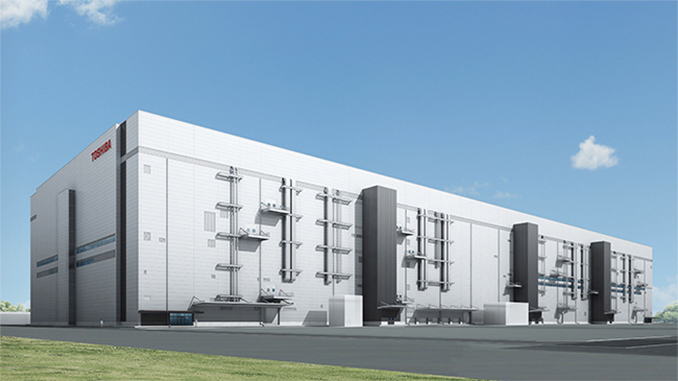
The new manufacturing facility near Kitakami (Iwate prefecture) will be Toshiba’s largest fab building ever and is expected to feature the highest manufacturing capacity as well, both because of expanded cleanroom space as well as a new production system that will use artificial intelligence. As usual, the building will feature protection against earthquakes that tend to happen in Japan.
Toshiba expects that construction of the new fab will be completed in autumn, 2019. After the company moves in equipment, the fab will come online sometimes towards the end of 2020. Meanwhile between now and late 2019, Toshiba will have to make decision regarding the equipment to be used in the fab and precise manufacturing capacity of the manufacturing facility.
The upcoming fab will complement Fabs 2 and 6 — the two contemporary fabs at the Yokkaichi Operations memory production complex in Mie Prefecture, which Toshiba jointly operates with Western Digital.
Toshiba is about to start using its Fab 6/phase 1 fab at the Yokkaichi Operations this summer. The move will help it to increase production of BiCS 3D NAND flash memory in the coming months. Next year the company is expected to deploy the Fab 6/phase 2 fab.
Buy Toshiba OCZ RD400 512 GB SSD on Amazon.com
Related Reading:
- Toshiba Memory to Build New Fab to Produce BiCS 3D NAND
- Toshiba Finalizes Plans for New 3D NAND Fab: Coming Online in 2019
- Toshiba to Build New Fab to Produce BiCS NAND Flash
- Toshiba Signs Deal To Sell Memory Business
- Western Digital, Toshiba And Bain Capital Settle Disputes Over Sale Of Toshiba Memory
- Toshiba To Proceed With Sale Of Memory Business To Consortium
More...
-
07-26-18, 07:02 AM #8416
Anandtech: Microsemi Announces SmartRAID Cards With On-Board Supercapacitors And Encr
Last year, Microsemi released a new generation of 12Gbps SAS controller chips, then incorporated them into a variety of SAS/SATA host bus adapter (HBA) and RAID cards under their Adaptec brand. Now, their SmartRAID family of advanced RAID cards is getting two new models that bring new features to the product line.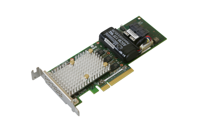
First up is the SmartRAID 3162-8i, which decodes to indicate a card with 8 internal ports and a 2GB DRAM cache with power loss protection. This is the first Adaptec RAID card to feature a fully-integrated power loss protection scheme including supercapacitors on the card itself. Previous SmartRAID cards such as the 3152-8i have all required an external supercapacitor module to be mounted in another expansion slot or elsewhere in the server. Putting supercapacitors on the half-height half-length card makes it fairly crowded and has the potential to restrict air flow across the controller, so Microsemi has upgraded many components on the card with industrial-grade parts rated for higher temperatures. This has also allowed Microsemi to spec the card for 150 linear feet per minute (LFM) of airflow instead of the 200 LFM required by the 3152-8i and similar cards.
The second new product is the SmartRAID 3162-8i/e, which uses the same hardware as above but is the first SmartRAID card to enable the encryption capabilities of the SmartROC 3100 controller chip. This controller-based encryption offers an alternative to using self-encrypting drives (SEDs) or software encryption on the host CPU. Microsemi brands this encryption system as maxCrypto, and touts its combination of the minimal performance overhead of SEDs with the flexibility of software encryption to support things like a mix of encrypted and unencrypted volumes, and re-keying or re-encrypting existing data in-place.
The encryption keys are derived using a master passphrase that generates a master key stored on the controller card. Each encrypted RAID volume created on the controller gets a separate volume encryption key generated by the master key. In the event that the RAID card dies, a replacement card can be swapped in and can reconstruct all the volume keys using the original master passphrase. The cipher used us AES256 in XTS mode.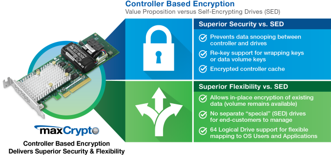
The new cards are in volume production now.
More...
-
07-26-18, 10:35 AM #8417
Anandtech: AMD Rome EPYC CPUs to Be Fabbed By TSMC
Along with AMD’s epic quarterly results that were announced yesterday afternoon, there was also an interesting nugget buried in the earnings call for the results. We’ve known for some time now that AMD was going to be working with both TSMC and fraternal fab GlobalFoundries to produce 7nm products, similar to what they’ve done for their current-generation 16nm/14nm products. However until now it hasn’t been clear how those products would be allocated – whether TSMC will once again just produce semi-custom APUs, or if they’ll do more. But now we have an answer thanks to AMD’s earnings call, and the answer is indeed “more”.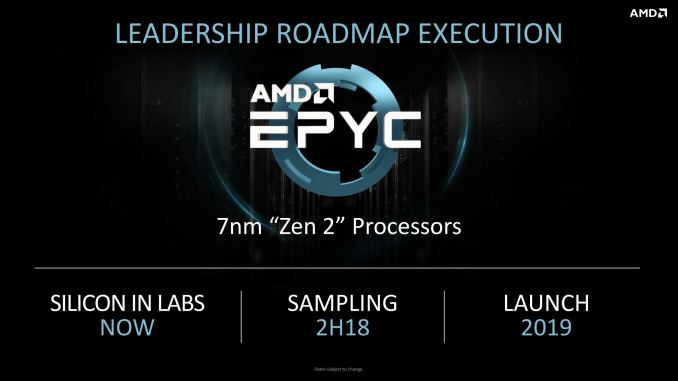
Specifically, AMD CEO Lisa Su has announced that second-generation “Rome” EPYC CPU that the company is wrapping up work on is being produced out at TSMC. This is a notable departure from how things have gone for AMD with the Zen 1 generation, as GlobalFoundries has produced all of AMD’s Zen CPUs, both for consumer Ryzen and professional EPYC parts.
So, Matt, on your first question relative to the manufacturing of the second generation of EPYC, so as I said earlier, we are working with both the TSMC and GLOBALFOUNDRIES in 7-nanometer. As for the 7-nanometer Rome that we're currently sampling, that's being manufactured at TSMC.As it stands, AMD seems rather optimistic about how things are currently going. Rome silicon is already back in the labs, and indeed AMD is already sampling the parts to certain partners for early validation. Which means AMD remains on track to launch their second-generation EPYC processors in 2019.
Unfortunately, the call offered no real insight as to why AMD has shifted to using TSMC for some of their CPUs for this upcoming generation. AMD’s hands are somewhat tied on fab choice in as much as they have quotas under their wafer share agreement with GlobalFoundries that they must fulfill. How AMD wants to split that up is up to them, but beyond that AMD hasn’t offered any information as to why they’ve made the choices they have.
Ultimately however if they are meeting their order quota from GlobalFoundries, then AMD’s situation is ultimately much more market driven: which fab can offer the necessary capacity and performance, and at the best prices. Which will be an important consideration as GlobalFoundries has indicated that it may not be able to keep up with 7nm demand, especially with the long manufacturing process their first-generation DUV-based 7nm “7LP” process requires.
More...
-
07-26-18, 10:35 AM #8418
Anandtech: AMD Announces Q2 2018 Results: Best Quarter In Seven Years
What a difference a year makes. Yesterday afternoon AMD announced their second quarter results for their fiscal year 2018, and the news is nothing short of stunning, with AMD having one of their best quarters in seven years. AMD already started off the year profitable, but things have continued to ramp up in Q2, marking the 1 year anniversary of the Zen CPU architecture launch, and the inflection point for AMD’s badly-needed recovery.
For Q2 AMD booked $1.76B in revenue, their greatest revenue in quite some time and beating not just their seasonally strong Q4 from last year, but also the cryptocurrency-fueled Q1 of this year. This is a massive 53% jump in revenue year-over-year, while even on a quarterly sequential basis that’s a 7% increase. As a result, both AMD’s profits and gross margins were up. Net income rose by $158M year-over-year to $116M – a far cry from the money-losing situation of AMD a year ago – while gross margins have risen to 37%.AMD Q2 2018 Financial Results (GAAP) Q2'2018 Q1'2018 Q2'2017 Revenue $1756M $1647M $1151M Gross Margin 37% 36% 34% Operating Income $153M $120M -$1M Net Income $116M $81M -$42M Earnings Per Share $0.11 $0.08 -$0.04
Looking at the non-GAAP numbers, which exclude results such as restructuring charges, debt fees, and stock based compensation, which are also strong. AMD continues to pay down its sizable long-term debt and issue stock as compensation, both of which bring down the GAAP numbers, but not extensively. More importantly it shows that AMD’s GAAP numbers themselves aren’t a fluke, and that AMD’s core business is stronger than it has been in quite some time.AMD Q2 2018 Financial Results (Non-GAAP) Q2'2018 Q1'2018 Q2'2017 Revenue $1756M $1647M $1151M Gross Margin 37% 36% 34% Operating Income $186M $152M $23M Net Income $156M $121M -$7M Earnings Per Share $0.14 $0.11 -$0.01
AMD is attributing the great quarter to what can best be described as all-around improved demand for products. Ryzen, Epyc, and Radeon shipments were all well up year-over-year, and even on a sequential basis AMD’s CPUs continue to be in high demand. AMD’s specifically citing the ramp of new products here (presumably Ryzen 2) as being especially beneficial towards the gross margin, and ultimately their bottom line.
Digging into the individual segments a bit more, the larger of AMD’s two segments, Computing and Graphics, booked $1.09B in revenue for the quarter. This is a 64% jump in revenue year-over-year, though a slight decline sequentially. Operating income was $117, which is over $100M better than last year, but again a bit of a drop over Q1. AMD credits the year-over-year shift to the significant growth of Ryzen products – this being the first Q2 where AMD has a top-to-bottom CPU and APU stack in place for desktop and mobile – while Radeon is a bit more of a mixed bag. AMD’s strong Q1 performance was in part built on top of the red-hot cryptocurrency market, which has significantly cooled in the last couple of months. This being why AMD’s numbers are down a bit on a quarterly basis, as overall GPU revenue has dropped.AMD Q2 2018 Computing and Graphics Q2'2018 Q1'2018 Q2'2017 Revenue $1086M $1115M $661M Operating Income $117M $138M $7M
The April launch of Ryzen 2 CPUs meant that AMD has seen “double digit” shipment growth in Ryzen processors over the previous quarter, on top of growth of Ryzen mobile APUs, where ships actually more than doubled. Consequently desktop processor ASPs are down, but mobile processor ASPs are actually up, presumably as customers shift away from bargain-priced Bristol Ridge parts. Interestingly GPU ASPs are also up, despite the cooling crypto market, with AMD citing datacenter sales as pulling ASPs up.
Meanwhile for the Enterprise, Embedded, and Semi-Custom market, AMD booked $670M in revenue for the year, up $180M from Q2 of 2017. Operating income is also up, though not as wildly as with computing products, rising from $16M to $69M. Notably, this segment includes AMD’s EPYC processors for datacenters. I’d been expecting first-generation EPYC sales to be soft as AMD needed to prove itself to customers who were burnt on the Bulldozer generation, however AMD has been consistently reporting good news here, as EPYC adoption continues to grow. Meanwhile the semi-custom side has also done better than expected thanks to some non-cancellable purchase orders.AMD Q2 2018 Enterprise, Embedded, and Semi-Custom Q2'2018 Q1'2018 Q2'2017 Revenue $670M $532M $490M Operating Income $69M $14M $16M
Overall then AMD had a very good quarter, and if the company has its way, this is the start of things to come. As energizing as the company’s success with Ryzen has been, the big money for the company is ultimately in high-margin datacenter products, including both EPYC and Radeon Instinct. The next-generation EPYC processors aren’t due until 2019, but there’s still time to grow the current generation, as EPYC revenue was up 50% sequentially over Q1. And indeed AMD is predicting that gross margins will tick up to 38% in Q3. Which is still a far cry from Intel’s traditionally massive margins, but is moving AMD where they need to be to be consistently and significantly profitable. Otherwise, AMD is predicting $1.7B in revenue for Q3, which would end up being very close to this Q2.
More...
-
07-26-18, 12:41 PM #8419
Anandtech: CRU Acquires ioSafe, Creating Disaster-Resistant Storage Powerhouse
CRU last week took over ioSafe, creating a company that owns both software and hardware assets to create disaster-resistant storage solutions. Given their different specialties, CRU and ioSafe do not have products that compete directly against each other, so the product lineups of both companies will continue to complement each other in CRU’s future family of devices.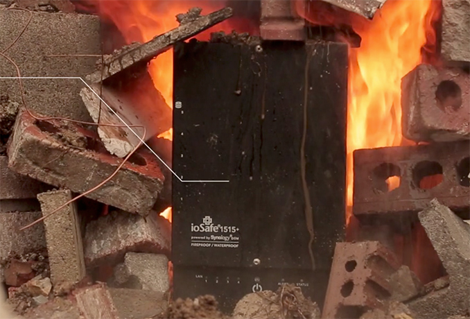
ioSafe sells fireproof and waterproof NAS and storage servers. This somtimes includes servers designed by other companies, such as Synology. ioSafe’s products are aimed at clients from military or manufacturing industries who need disaster-resistant storage solutions and in some cases are tailor-made. By contrast, CRU develops and builds its products in house and specializes on rugged storage solutions for audio/video production, business markets, digital forensics investigators and so on.
While products from ioSafe and CRU serve the same purpose of protecting data, they are aimed at different customers and sometimes even industries. Which means that while there's overlap in terms of technology, there's very little overlap in terms of customers. After the acquisition ioSafe will retain its team and product families. Meanwhile, what remains to be seen is how ioSafe will continue to work with its external partners.
By taking over ioSafe, CRU gains experience in creating storage devices with superior protection against fire, water, chemical, altitude and other kinds of disasters and environments.
Related Reading:
- ioSafe Launches BDR 515 Backup and Disaster Recovery Appliance
- CRU ToughTech Duo C Storage Enclosure (2x 2.5" to USB 3.1 Gen 2 Type-C) Review
- ioSafe Updates Disaster-Resistant Storage Lineup at CES 2015
- ioSafe 1513+ Review: A Disaster-Resistant Synology DS1513+
- ioSafe N2: A Disaster-Resistant Synology DS213
More...
-
07-26-18, 10:57 PM #8420
Anandtech: Intel 10nm Production Update: Systems on Shelves For Holiday 2019
Earlier this year Intel confirmed that it would delay mass production of 10nm CPUs to 2019 due to issues with yields, but did not elaborate on when in 2019 that would be. Late on Thursday Intel finally made a long-awaited clarification: the first systems powered by 10nm CPUs will hit store shelves in the second half of 2019. But there is a catch: 14nm products will still continue to play a big role next year.
Intel is set to start mass production of processors using its 10nm process technology in 2019, and while the company isn't explicitly saying when mass production will begin, it's sounding like that will be in the Q2/Q3 time frame. This being based off of what Intel is saying, which is that they expect to have PCs based on these chips to arrive during the 2019 holiday shopping season. Given the kind of lead-time required to get complete OEM systems on to store shelves, this would mean that mass production on chips needs to start 3 to 6 months sooner than that.
As for said finished systems, what's typically considered the holiday shopping season starts in October or early November. So systems based on Intel’s 10nm CPUs would finally be available in mass quantities starting in Q4 of 2019. Consequently, for more three quarters of next year Intel will continue to rely almost entirely on its products made using its various 14nm process technologies.
It remains to be seen how much time it will take Intel to ramp up production of its 10nm CPUs and when the volume crossover between 14nm and 10nm chips occurs. At present, Intel seems to be optimistic about what it has today and will have tomorrow — a variety of 14nm products. In fact, there is a lot of room for growth here: shipments of Intel’s Xeon Scalable processors accounted for a little less than 50% of Intel’s datacenter revenue in the most recent quarter, so the company will certainly continue to ramp up shipments of these products for many quarters to come, increasing its ASPs and revenue. Keep in mind that Intel’s upcoming Cascade Lake-SP platform will bring support for 3D XPoint-based Optane DC Persistent Memory DIMMs, which will bring in huge earnings opportunities to the company.
Speaking of datacenter products. Murthy Renduchintala, Intel’s chief engineering officer, promised that 10nm “datacenter products” will follow “shortly after” availability of client systems running 10nm CPUs in the late 2019. He did not give any exact timeframes, but stressed that its next-gen Xeon will follow its next-gen client parts quicker usually. Essentially, Intel confirmed this week’s report claiming that the codenamed Ice Lake-SP CPUs may hit the market in Q3 or Q4 of 2020.
Note: Image of a wafer is for illustrative purposes only.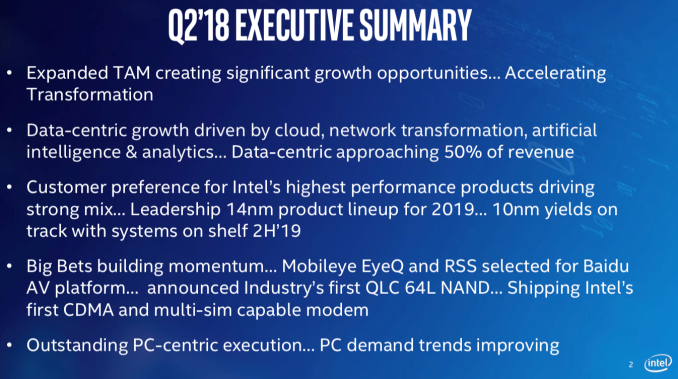
Related Reading:
- Intel Delays Mass Production of 10nm CPUs to 2019
- Intel’s Xeon Scalable Roadmap Leaks: Cooper Lake-SP, Ice Lake-SP Due in 2020
- First 10nm Cannon Lake Laptop Spotted Online: Lenovo Ideapad 330 for $449
- Intel Discloses Plans to Spend $5 Billion on Fab 28 Expansion in Israel
- Intel's 10nm Briefly Appears: Dual Core Cannon Lake in Official Documents
- Intel Mentions 10nm, Briefly
- Intel Displays 10nm Wafer, Commits to 10nm ‘Falcon Mesa’ FPGAs
More...


 Quote
QuoteThread Information
Users Browsing this Thread
There are currently 17 users browsing this thread. (0 members and 17 guests)


Bookmarks