

Results 8,831 to 8,840 of 12094
Thread: Anandtech News
-
11-13-18, 05:05 PM #8831
Anandtech: Imagination Launches PowerVR Automotive Initiative, 8XT-A GPU IP
The automotive industry is changing rapidly these days thanks to the influx of computing poweer, and it will continue to consume considerably more CPU and GPU horsepower in the coming years. As a result, it is not surprising that IP and hardware developers are increasingly tailoring offerings for the automotive industry. To that end, Imagination Technologies on Tuesday introduced its PowerVR Automotive package of IP aimed specifically at solutions for various vehicles. In fact, PowerVR Automotive is more like an initiative that will expand over time to include more offerings.
Imagination has been supplying various IP blocks for the automotive semiconductor industry for many years, so the company is clearly not a newbie here. Today, PowerVR IP — including 8XT high-performance GPU cores, energy-efficient 8XT/P GPU IP, and 2NX neural network accelerator IP — are used extensively for chips that power infotainment, digital cockpit, and advanced driver assistance systems (ADAS). Meanwhile, as demands from developers of SoCs for auto applications are growing, Imagination is rolling out its new portfolio of IP featuring enhancements specifically aimed at the automotive industry.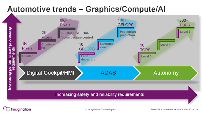
Gallery: Imagination Launches PowerVR Automotive Initiative, 8XT-A GPU IP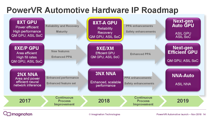


Imagination’s 2018 portfolio of PowerVR Automotive hardware IP includes the PowerVR 8XT-A GPU, which supports enhanced recovery and reliability features that are required by SoC designers to get automotive safety certification for processors aimed at digital human-machine interfaces (HMIs) and autonomous vehicles (AVs). In particular, SoCs featuring the 8XT-A GPU achieve ASIL-levels of functional safety, and can meet industry standards such as ISO 26262 as well as IEC 61506. The new GPU also supports hardware virtualization for QoS and security (i.e., all apps can run in isolated containers), ECC, and LBIST (logic built-in self-test). Meanwhile for those who need an ultimate reliability and do not care about the costs, the PowerVR 8XT-A even supports a dual GPU technology that enables to run workloads in lockstep.
Besides enhancing the GPU on the logical level, Imagination claims that it also ensures that the IP is implemented using a process technology that is tailored for automotive applications too (so, think extended temperature ranges and other perks).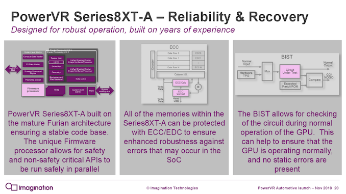
In addition to the PowerVR 8XT-A GPU, the 2018 automotive hardware IP portfolio from Imagination also includes the PowerVR 9XE/XM energy-efficient GPU, as well as the 3NX neural network accelerator. What is more important is that Imagination intends to continue to expand its PowerVR automotive hardware IP portfolio with tailored solutions. In addition to another automotive-grade GPU IP due next year, the company will offer an ASIL-capable NNA. Which in turn can be mixed and matched with the PowerVR 8XT-A GPU and other processing blocks.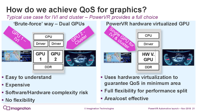
All of Imagination’s PowerVR Automotive IP is supported by appropriate APIs, hypervisors, operating systems, and so on. Therefore, a broad lineup of SoC developers as well as auto makers can take advantage of the new IP designed by Imagination.
Related Reading:
- Imagination Technologies to Be Acquired by Canyon Bridge for £550M; MIPS Sold to Tallwood VC
- Imagination Announces PowerVR Series 8XT GT8525: Their First Furian GPU Design
- Imagination Announces PowerVR Furian GPU Architecture: The Next Generation of PowerVR
Source: Imagination Technologies
More...
-
11-13-18, 05:05 PM #8832
Anandtech: G.Skill Unveils 64 GB DDR4-4266 and 128 GB DDR4-4000 Kits for HEDTs
Coinciding with today’s launch of Intel’s HEDT “Skylake-X/Basin Falls Refresh” family of CPUs, G.Skill today announced its new 64 GB DDR4-4266 and 128 GB DDR4-4000 kits designed for high-end desktops.
G.Skill’s new Trident Z quad-channel memory includes a 64 GB (8×8 GB) kit rated to run at DDR4-4266 CL19 19-19-39 with 1.45 Volts, and a 128 GB (8×16 GB) set designed to operate at DDR4-4000 CL19 19-19-39 with 1.35 Volts. The DIMMs are based on Samsung’s time-proven B-die memory chips that are used for overclocking-grade modules, feature XMP 2.0 SPD profiles for easier set up, and are outfitted with aluminum heat spreaders.
Since we are dealing with very high-performance SKUs, G.Skill requires them to run on high-end motherboards capable of delivering a “clean” power supply and keep the amount of interference at minimal levels. So far, G.Skill has validated the kits with the ASUS Prime X299-Deluxe II motherboard, though the list of "officially" compatible platforms may expand over time.G.Skill's Trident Z Memory for Intel's Skylake-X Speed CL Timing Voltage Kit
Config.Kit
CapacityFamily DIMM PN DDR4-4000 CL19 19-19-39 1.35 V 8×16 GB 128 GB Trident Z RGB ? DDR4-4266 CL19 19-19-39 1.45 V 8×8 GB 64 GB Trident Z ?
One thing to note about the 64 GB DDR4-4266 1.45 V kit is that it runs at a voltage that is 20% over DDR4 standard's default voltage of 1.2 V, which means that power consumption of the kit will be noticably higher than standard modules (keep in mind that power consumption increases with the square of the voltage). Therefore, the kit will require good cooling as well. In the meantime, the 128 GB kit will also use a fair bit of power simply because of its capacity.
G.Skill plans to start sales of its new Trident Z 64 GB DDR4-4266 and 128 GB DDR4-4000 quad-channel memory kits sometime in the first quarter of 2019. Along those lines, since they're still a quarter out from launch, the company has not announced the pricing of the new products, as that will depend on the spot price of DRAM at the time. Meanwhile, given the performance and capacities of the modules, expect the kits to carry a premium price tag.
Related Reading: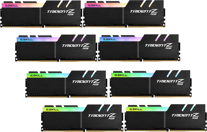
- The Intel Core i9-9980XE CPU Review: Refresh Until it Hertz
- G.Skill’s DRAM Extremes: DDR4-4000 on AMD Ryzen, DDR4-5066 on Intel Core i7
- G.Skill Announces Quad-Channel DDR4-4200 Kit for Intel Skylake-X CPUs
- DRAM and Motherboard Makers Demonstrate Quad-Channel DDR4-4000+ Operation
Source: G.Skill
More...
-
11-13-18, 06:08 PM #8833
Anandtech: AMD 64-Core Rome Deployment: HLRS Hawk at 2.35 GHz
Last week AMD pre-announced its next-generation EPYC processors, code-named Rome. These new processors are set to be officially announced next year, but will feature up to 64 cores using eight 7nm chiplets surrounding a central 14nm IO die. This week is the annual Supercomputing conference, focusing on high-performance computing, where all the big OEMs with server offerings as well as supercomputing centers get to promote their latest and greatest. One of them is the High Performance Computing Center based in Stuttgart, Germany, who disclosed some information about their new ‘Hawk’ system.
More...
-
11-14-18, 05:48 AM #8834
Anandtech: Samsung Announces 8nm Exynos 9820 With Tri-Group CPU Design
Early this morning Korea time, Samsung LSI announced their newest generation flagship SoC, the Exynos 9820.
The Exynos 9820 succeeds this year’s Exynos 9810, which we’ve covered extensively both in our review of the Galaxy S9, as well investigated in separate pieces, ending with an official microarchitectural disclosure of the M3 core at HotChip 2018.
The Exynos 9810 was not a very successful chip, as the M3 microarchitecture as well as the implementation had some severe flaws, with actual devices based on the chip largely lagging behind their Snapdragon counter-parts, having to sacrifice a lot of performance in order to keep up with battery efficiency, and even then, failing to do so most of the time.
The Exynos 9820 looks to rectify this situation with a new design and new CPU configuration, but let’s go over the specifications first:
The new 9820 now fundamentally changes the CPU configuration from a 4+4 setup, to a 2+2+4 setup, where we now have two fourth generation Samsung CPUs as the top performing units, two Cortex A75 CPUs as the mid-tier performance cores, and four Cortex A55 CPUs for maximum power efficiency.Samsung Exynos SoCs Specifications SoC Exynos 9820 Exynos 9810 CPU 2x M4? @ ? GHz
It does have L2
2x Cortex A75 @ ? GHz
Probably L2
4x Cortex A55 @ ? GHz
Let's hope it has L2
Shared complex L3 @ =>4MB4x M3 @ 1c2.7 / 2c2.3 / 4c1.8 GHz4x 512KB L2
4096KB L3
4x Cortex A55 @ 1.8 GHz
no L2
512KB L3GPU Mali G76MP12 Mali G72MP18 Memory
Controller4x 16-bit CH
LPDDR4x @ ?MHz4x 16-bit CHLPDDR4x @ 1794MHzMedia 8K30 & 4K150 encode & decode
H.265/HEVC, H.264, VP910bit 4K120 encode & decodeH.265/HEVC, H.264, VP9Modem Shannon Integrated LTE
(Category 20/13)
DL = 2000 Mbps
8x20MHz CA, 256-QAM
UL = 316 Mbps
3x20MHz CA, 256-QAMShannon Integrated LTE
(Category 18/13)
DL = 1200 Mbps
6x20MHz CA, 256-QAM
UL = 200 Mbps
2x20MHz CA, 256-QAMISP Rear: 22MP
Front: 22MP
Dual: 16MP+16MPRear: 24MP
Front: 24MP
Dual: 16MP+16MPMfc.
ProcessSamsung
8nm LPPSamsung
10nm LPP
First of all, the new CPU configuration is rectifying one of the issues of the Exynos 9810: Here, the A55 cores were on a separate cluster block on the SoC, and thus cache coherency to the performance cores had to go through the SCI/interconnect, which undoubtedly impacted efficiency. On the Exynos 9820, all CPUs, including the Cortex CPUs, are now integrated within the same cluster and the new L3 is a cache hierarchy to all CPUs, undoubtedly not only improving power efficiency, but also performance of the smaller cores now.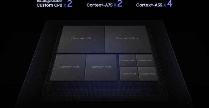
The new L3 cluster is very much similar to Arm’s DynamIQ DSU, however it’s of Samsung’s own design as Arm doesn’t allow third-party cores to plug into the DSU.
The choice of a Cortex A75 as a mid-tier CPU group is evident: Having four big cores such as the M3 or evidently the M4 is very much a waste of die space because in a mobile power envelope, the four cores will never be able to operate at their maximum frequency / performance. So instead of using the same big microarchitecture at a lower clocked configuration, it makes sense to just use a smaller CPU and regain some of the die space. What this also allows Samsung to do is to further optimise the big custom cores for peak frequencies and performance as they no longer have to value the lower-end of the power curve as much- which is now covered by the A75’s.
In terms of the new fourth generation custom CPU, the M4 (If they’ll end up naming it like that) is advertised to have “enhanced memory access capability”. As we’ve covered the microarchitectural disclosure of the M3, Samsung did admit the cache hierarchy was one of the last pieces that was designed for the IP, and it seemed evident that there were some compromises made. The memory hierarchy and the memory subsystem of the M3 did seem the Achilles heel of the microarchitecture, as it seems to prevent the core reaching higher performance levels that you’d expect from such a wide core.
The new M4, as per the marketing materials, now promises a 20% boost in performance, or a 40% increase in power efficiency when compared to the Exynos 9810. I’m still working on the review of the Mate 20’s and the new Cortex-A76 sporting Kirin 980, which should be published soon enough, but these improvement claims from Samsung do not seem sufficient to be able to remain competitive and catch up to the Cortex A76. Here Samsung would need to both showcase a 20% improvement in performance, while at the same time improving power efficiency by 50% in order to catch up with the Kirin 980. Unfortunately the gap currently seems far too big for the 9820 to be able to overcome, unless of course it beats the advertised marketing figures.
One thing that S.LSI didn’t announce today was any kind of frequencies. For the Exynos 9810 they had chosen to advertise some unrealistically high clocks of “up to 2.9GHz”, however these weren’t achievable without some absurd power figures. Along with the IPC upgrades of the new core, I’m expecting the M4 to remain in the 2.5-2.7GHz range, with Samsung hopefully abstaining from going too high in the far end of the voltage curve. The Cortex A75’s should hopefully be in the lower 2GHz range in order to also take advantage of the better efficiency points.
A bigger GPU configuration - Arm's Mali G76MP12
On the GPU side of things, the Exynos 9820 now offers Arm’s new Mali G76 in an MP12 configuration. This represents a 33% increase in the execution engines over the G72MP18 of last generation, and Samsung materials advertise a 40% increase in performance at the same power, or a 35% increase in efficiency at the same performance. On the Kirin 980 the new G76 made some very large improvements, however it just missed the mark in terms of my projections. However S.LSI was always able to achieve much better results than HiSilicon, so the new G76 in the 9820 might very well end up being respectable, even though again I’m not expecting it to match up again Apple’s best and Qualcomm’s next generation.
A new dedicated NPU, alongside connectivity and media improvements
The new 9820 also features a new first for S.LSI: The new chip now for the first time features an NPU (Neural Processing Unit). Details of the new IP are severely lacking, and all we know about it is that Samsung promises it being used for enhancing photo captures or use-cases such as AR, and it to be "7x faster" than the Exynos 9810 in its tasks.
In terms of media capabilities, the new SoC’s encoder IP now promises 8K30 capability. Now I’m not really expecting new devices to be able to be able to capture in this mode as it’ll also require camera sensor support – but having a robust media encoder like this can also point out to improved recording power efficiency.
The new modem now features LTE connectivity up to Category 20 in download and upload, achieving up to 2Gbps at 8CA in downstream and 316Mbps at 3CA in upstream.
One thing that Samsung didn’t highlight in its announcement but is listed in the specifications, is the fact that the SoC now support UFS 3.0 storage. The new standard will be able to double up on the transfer speeds compared to UFS 2.1, achieving a theoretical max of 2.9GB/s.
8nm LPP Manufacturing node
Lastly, but not least, the new Exynos 9820 is manufactured on an 8nm LPP process node from Samsung. 8LPP is an evolution of 10LPP and promises improved power consumption by up to 10%. Here the advertised improvements are relatively meagre, and some people will be questioning if this will be enough to compete with TSMC 7nm node in the current Kirin 980 as well as the upcoming Snapdragon. While it does look like Samsung will have a density disadvantage, I’m not expecting the performance and power disadvantage to all that dramatic. Still, the Exynos 9820 will have a tough time this year, both on the microarchitectural and process node side.
Overall – the new Exynos 9820 should bring much needed improvements compared to its predecessor, however the competition this year will be extremely tough. Here I do hope Samsung makes the best of the silicon and is able to also have a good software stack, as the new tri-group CPU configuration will need a good scheduler. The new Exynos 9820 is planned to go into mass production by the end of the year, and we’ll evidently see it next spring in the new Galaxy S10.
Related Reading- The Samsung Galaxy S9 and S9+ Review: Exynos and Snapdragon at 960fps
- Improving The Exynos 9810 Galaxy S9: Part 1
- Improving The Exynos 9810 Galaxy S9: Part 2 - Catching Up With The Snapdragon
- Hot Chips 2018: Samsung’s Exynos-M3 CPU Architecture Deep Dive
- Samsung Announces New 9810 SoC: DynamiQ & 3rd Gen CPU
- The Samsung Exynos M3 - 6-wide Decode With 50%+ IPC Increase
- JEDEC Publishes UFS 3.0 Spec: Up to 2.9 GB/s, Lower Voltage, New Features
More...
-
11-14-18, 07:41 AM #8835
Anandtech: The Windows 10 October 2018 Update (1809): Let's Try This Again
Back on October 2nd, Microsoft announced general availability for the latest update to Windows 10, the Windows 10 October 2018 Update. The new naming is improved over what they’d been doing in the past, where updates were called Creators Update or Fall Creators Update, and hopefully this continues. As a version, this update is Windows 10 1809.
More...
-
11-14-18, 09:28 AM #8836
Anandtech: AnandTech Forums XenForo 2.0 Upgrade Today (11/14)
For our forum regulars who may be wondering what’s going on – or even just onlookers who are curious as to what’s up at AnandTech – you’ll want to know that we’re giving the AnandTech Forums a well-deserved upgrade today to XenForo 2.0. As a result of the upgrade, the Forums will be in read-only mode for most of the day, as we’re expecting the upgrade to take into the evening.
Behind the scenes, the community and dev teams are in the process of upgrading our forums from XenForo 1.5 to XenForo 2.0. A medium-sized update, the latest version of XenForo adds several features that the community team is eager to get deployed, including quick thread replies, a better user interface (including keyboard navigation!), HiDPI images, and of course forum load time improvements.
We’re expecting this to take around 12 hours – wrapping up at around 9pm EST – however as with any big server update, this is subject to change depending on how well the process goes. In particular, the AnandTech Forums user and post history goes back nearly 20 years (dating back to October of 1999), so there’s a significant amount of content to bring over. So for the purpose of the upgrade the Forums will be in read-only mode so that the dev team can more easily move content over.
In the meantime you’re welcome to read the Forums, or hang out in the AnandTech comments section. And if you’re not already an AnandTech Forums regular, then let this serve as a not-so-subtle reminder that you should really join our Forums and connect with one of the best tech communities on the Internet.
More...
-
11-14-18, 01:03 PM #8837
Anandtech: Google Rolls Out Night Sight Tech to Improve Quality of Low-Light Photos
Google on Wednesday began to roll out its Night Sight low-light computational photography technology to its Pixel-branded smartphones. The technology is designed to improve the quality of low-light photos, though with one significant caveat: it cannot handle moving objects.
As noted on our recent Pixel 3 smartphone review, one big thing brought by the latest generation of Google’s handsets is computational photography, which currently supports two modes to improve the picture quality of still pictures: Super Res Zoom, and Night Sight. As the names imply, the first one promises to introduce a superior zoom, whereas the second one enhances lighting. Both algorithms capture multiple temporally different images by the same sensor, then blend them and apply a special filter to either increase the spatial resolution or image exposure (without adding noise). Since the algorithms capture multiple pictures in burst mode, when something in the frame is moving, the Night Sight mode produces a motion blur effect on the picture rather than improve quality.
Despite its limitation, in our testing we saw that Night Sight brought rather dramatic enhancements to still images, to the point where flash lighting might not be needed for low-light conditions (think museums, for example, where flash photography is either prohibited or makes no sense because items are covered by glass).

Google’s Night Sight mode will be initially available only on the company’s own Pixel handsets (all generations). Though Google may end up having to play a game of cat & mouse, as ROM hackers have been able to modify imaging applications to get it working on third-party phones as well.
Related Reading:
- The Google Pixel 3 Review: The Ultimate Camera Test
- Hands On With Google’s Pixel 2 XL: More Pixels, More Google
- The Google Pixel XL Review: Life After Nexus
- Google Announces Pixel and Pixel XL Phones: Snapdragon 821, 5" & 5.5" Screens, $649, Preorders Start Today
Source: Google
More...
-
11-14-18, 03:22 PM #8838
Anandtech: OWC Announces 14-in-1 Thunderbolt 3 Dock: Now with microSD, 85 W Power Del
OWC this week introduced its new flagship Thunderbolt 3 dock, which features 14 ports. Living up to its flagship aspirations, the “one dock to rule them all” can also deliver 85 W of power, giving it enough power to drive a 15.6-inch laptop. When compared to a similar dock launched about a year ago, the new one loses a FireWire port, but gains a microSD slot along with a 10 Gbps USB 3.1 Gen 2 Type-C connector.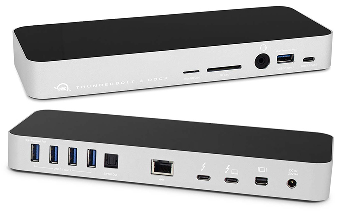
Just like its predecessor, the new OWC Thunderbolt 3 14-in-1 dock is aimed at professionals who use laptops, yet also own a high-resolution display (or two) along with multiple peripherals. The key feature of docks with over a dozen of ports is to keep everything — monitors, a keyboard, audio equipment, GbE, external storage, professional devices, and so on — connected to one device. When the owner comes with their notebook, all they have to do is to plug a single cable to the PC.
Without further ado, let us move on to what exactly the OWC Thunderbolt 3 14-in-1 dock offers. When it comes to common ports, the dock has five USB 3.1 Gen 1 Type-A connectors accompanied by one USB 3.1 Gen 2 Type-C port. Furthermore, the dock also has two Thunderbolt 3 ports (one for input) along with a miniDisplayPort 1.2, giving it the ability to drive two 4K monitors as well as a high-performance TB3 peripherals (storage, eGPU, etc.). Accompanying the mDP is a Gigabit Ethernet jack, which is quite popular in both consumer and business environments.
Moving on to less common connectors (at least when it comes to docking stations). The device also has an SD card and a microSD card reader (unfortunately, supported speeds are unknown), one is aimed at professional photographers, another is designed for those who use various emerging devices like drones. Speaking of professionals, it is necessary to note that the Thunderbolt 3 14-in-1 dock also has an S/PDIF output, and an additional 3.5-mm audio in/out to connect speakers, mics, headsets, and other equipment.
One important advantage of the OWC Thunderbolt 3 14-in-1 dock over its predecessor is its ability to deliver up to 85 W of power over a Thunderbolt 3 interface. By contrast, the model launched in 2017 only could deliver 60 W of power, which is enough for a 13.3-inch laptop (e.g., MacBook Pro 13.3), but clearly not sufficient for a 15.6-inch notebook (e.g., MacBook Pro 15.6).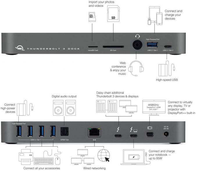
Considering the number of ports that the new 14-in-1 OWC Thunderbolt 3 dock has, it is evident that it has at least five controllers/bridges (USB 3.1 Gen 1, USB 3.1 Gen 2, GbE, audio, SD) along with power ICs, and other necessary chips inside. As a result, OWC's new flagship dock has a flagship price, hitting the shelves at $299.99. In the meantime, its predecessor with FireWire can now be acquired for $249.99.
Related Reading:
- OWC Ships ThunderBlade External SSDs, Touts SoftRAID Tech for 3800 MB/s Speeds
- OWC Launches 13-Port Thunderbolt 3 Dock: GbE, USB-A, SD Card, mDP, FireWire & More
- AKiTiO Thunderbolt 3 Dock Pro with Aquantia 10 GbE
- Corsair Launches Elgato Thunderbolt 3 Mini Dock
- StarTech Launches ‘Affordable’ Thunderbolt 3 ‘Mini Docks’: USB-A, GbE, DP or HDMI
- StarTech’s New Adapter Brings eSATA Storage to Thunderbolt 3 PCs
Source: OWC
More...
-
11-14-18, 03:22 PM #8839
Anandtech: ASUS Comments on Intel Shortages, U.S.-China Trade War
ASUS this week released its financial results for the third quarter of the year, and in the process issued comments regarding two pressing issues: shortages of Intel’s chipsets and processors, as well as the ongoing trade dispute between the U.S. and China. As it turns out, the situation is tough in both cases: tight supply will persist for quarters, whereas the trade feud may force ASUS and other companies to relocate its production facilities from China to other countries.
Shortages of Intel CPUs to Persist Through Q2 or Q3 2019
As reported, high demand for high-profile products has increased pressure on Intel’s factory network and forced the chipmaker to prioritize fabrication of its high-margin large-die Core and Xeon CPUs over other products in the recent months. Consequently, shipments of entry-level products made using 14 nm process technology are tight right now. In a bid to tackle the problem, Intel is in the process of allocating $1 billion to boost production of chips at its manufacturing facilities located in Oregon, Arizona, Ireland, and Israel. Meanwhile, it takes months to install new equipment into fabs, so any new step-and-scan tools acquired this quarter will unlikely have any impact on fab throughput until end of Q1 next year. ASUS certainly knows about that and admits that it expects tight supply to persist till Q2 or Q3 2019.
“We cannot answer on behalf of Intel,” said Jerry Shen, chief executive ASUS during the company’s earnings conference. “For example, data center will be the priority for Intel shipments, but priority is something we cannot answer on behalf of Intel. The shortage will affect component levels the most, such as the motherboard. Currently we believe that this will not be resolved before the Q2 of next year. Perhaps, it will be resolved in Q3 of next year. So, from now to next year we face many uncertainties in terms of CPU shortages.”
One thing to keep in mind here is that the first two quarters of the year are usually not big for PC shipments, so if ASUS is correct in its assumption that shortages will persist until Q3, this may indicate that there is a backlog of chips that Intel will have to ship in the coming quarters. Meanwhile, ASUS does not expect the chip giant to fulfill these orders for a while.
When asked whether ASUS could offset shortages of Intel processors with AMD chips, the company said that it would certainly use more CPUs from AMD, but mainly for markets where acceptance of such products is high enough.
U.S.-China Trade War May Force ASUS to Relocate Some Production Capacities
Another pressing issue that ASUS management had to address is of course the ongoing trade conflict between the U.S. and China. The short-term problem that ASUS is facing is currency fluctuations and the need to hedge risks, which has an effect on already thin profit margins. However, longer-term problems could be far more challenging.
The tariffs imposed by the U.S. on China-made goods may force not only ASUS, but also other hardware makers to relocate some of their Chinese production capacity to other countries. ASUS is currently considering Taiwan, Vietnam, and other countries in Southeast Asia as candidates for relocation. In fact, the company already has production facilities in Taiwan, but the question is whether it has enough capacity to meet current demand for components, or will have to invest in expansion.
In addition to moving production facilities, hardware producers may need to switch to other suppliers of components. Right now, ASUS is considering the relocation of its own PC components manufacturing as an urgent matter. In other words, if the company moves assembly of, say, graphics cards and motherboards outside of China, it will also have to find new suppliers of small parts like capacitors, connectors, sockets, and so on.
As for impact on pricing of ASUS-branded hardware, the head of the company said that the manufacturer would make its best effort to maintain its market leadership in a bid to be able to determine prices. In fact, the company stressed that a plain increase of notebook prices would not work without increasing their value for the end user, particularly in well-developed regions like Europe and the U.S.
To sum up, there are a number of changes that are happening on the market right now, though the exact results of these changes remain to be seen.
Related Reading:
- Intel Investing $1B to Meet 14nm Demand: Prioritizing High-End Core and Xeon
- Intel Announces Q3 FY 2018 Earnings: Record Quarter
- Intel to Split Manufacturing Group into Three Segments
- Intel Announces 9th Gen Core CPUs: Core i9-9900K (8-Core), i7-9700K, & i5-9600K
Source: ASUS
More...
-
11-15-18, 07:00 AM #8840
Anandtech: SK Hynix Develops First 16 Gb DDR5-5200 Memory Chip, Demos DDR5 RDIMM
SK Hynix on Thursday announced that it had completed development of its first DDR5 memory chip. The new chip offers a capacity of 16 Gb and is said to be the industry’s first DRAM that is fully compliant with the JEDEC standard, which is yet to be published. Meanwhile, mass production of SK Hynix's DDR5 memory chips is slated for 2020.
The new DDR5 chip from SK Hynix supports a 5200 MT/sec/pin data transfer rate, which is 60% faster than the 3200 MT/s rate officially supported by DDR4. Meanwhile the DRAM operates at 1.1 Volts, a 9% decrease in operating voltage. The monolithic 16 Gb chip is made using SK Hynix’s second generation 10 nm-class process technology (also known as 1Ynm), though the company does not disclose its die size and other peculiarities.
Looking forward, SK Hynix expects its DDR5 lineup to include DRAM chips at 8 Gb, 16 Gb, and 32 Gb capacities, with data transfer rates ranging from 3200 to 6400 MT/s.
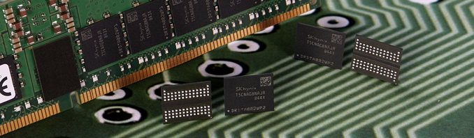
Besides announcing the memory chip, SK Hynix also demonstrated the industry’s first DDR5 Registered DIMM. The DDR5-5200 RDIMM module offers a peak memory bandwidth of 41.6 GB/s, which is in line with DDR4 modules overclocked to their extremes (using LN2-cooled CPUs, etc.). The DDR5 RDIMM itself features 288 pins on a slightly curved edge connector (to reduce the insertion force on every pin), yet its layout and design are a bit different when compared to DDR4 to avoid insertion of DDR5 modules into DDR4 slots and vice versa.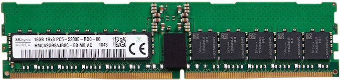
SK Hynix said that it had already shipped DDR5 RDIMMs and UDIMMs to a “major chipset maker” (Intel?) to assist in the development of server and client platforms supporting the new type of memory.
SK Hynix intends to start mass production of DDR5 memory sometimes in 2020, when the aforementioned platforms (at least one of them) are expected to hit the market.
Overall, JEDEC expects DDR5 to bring in I/O speeds ranging from 4266 to 6400 MT/s, with a supply voltage drop to 1.1 V and an allowable fluctuation range of 3% (i.e., at ±0.033V). Along with the performance improvements, the new memory standard also stands to improve in total capacity and DIMM density, with chips planned for 16Gb and beyond.
Under the hood, the new standard will will also bring several major enhancements to the design of memory modules, with the goal of improving their real-world performance and enabling higher data transfer rates. For example, each DDR5 DIMM will feature two independent 32/40-bit channels (without/or with ECC). Furthermore, DDR5 will have a better command bus efficiency (as the channels will have their own 7-bit Address (Add)/Command (Cmd) buses), better refresh schemes, and an increased bank group for extra performance.
Last month Cadence said that enhanced functionality of the standard will enable DDR5 to offer a 36% higher real-world bandwidth vs. DDR4 at the same data transfer rate. While we will not be able to test this claim before 2020, the improvements of DDR5 compared to the predecessor certainly look impressive.
Related Reading: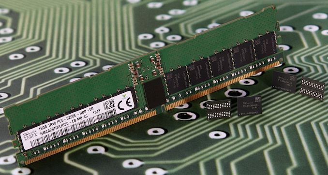
- Cadence & Micron DDR5 Update: 16 Gb Chips on Track for 2019
- Cadence and Micron Demo DDR5-4400 IMC and Memory, Due in 2019
- JEDEC: DDR5 to Double Bandwidth Over DDR4, NVDIMM-P Specification Due Next Year
Source: SK Hynix
More...


 Quote
QuoteThread Information
Users Browsing this Thread
There are currently 20 users browsing this thread. (0 members and 20 guests)


Bookmarks